Sony HT-NT3 Service Manual
Hide thumbs
Also See for HT-NT3:
- Operating instructions manual (204 pages) ,
- Startup manual (2 pages) ,
- Quick start manual (2 pages)
Table of Contents
Advertisement
SERVICE MANUAL
Ver. 1.1 2015.05
• All of the units included in the HT-NT3 (SA-NT3/SA-
WNT3) are required to confi rming operation of SA-NT3.
Check in advance that you have all of the units.
COMPONENT MODEL NAME
Bar Speaker (Active Speaker System)
Subwoofer (Active Subwoofer)
Amplifi er section
US model only:
POWER OUTPUT AND TOTAL HARMONIC
DISTORTION:
(FTC)
Front L + Front R:
With 4 ohms loads, both channels driven, from
300 Hz – 20,000 Hz; rated 50 watts per channel
minimum RMS power, with no more than 1% total
harmonic distortion from 250 milliwatts to rated
output.
POWER OUTPUT (reference)
Front L/Front R:
133 W (per channel at 4 ohms, 1 kHz)
Except US model:
POWER OUTPUT (rated)
Front L + Front R:
60 W + 60 W (at 4 ohms, 1 kHz, 1% THD)
POWER OUTPUT (reference)
Front L/Front R:
133 W (per channel at 4 ohms, 1 kHz)
Inputs
HDMI IN 1*/2/3
TV (DIGITAL IN)
ANALOG IN
Output
HDMI OUT* (ARC)
9-890-666-02
Sony Corporation
2015E81-1
©
2015.05
Published by Sony EMCS (Malaysia) PG Tec
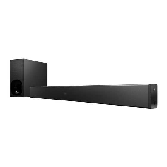
Photo: SA-NT3
HT-NT3
SA-NT3
SA-WNT3
SPECIFICATIONS
* HDMI IN 1 and HDMI OUT jacks support HDCP 2.2
protocol. HDCP 2.2 is newly enhanced copyright
protection technology that is used to protect content
such as 4K movies.
HDMI section
Connector
Type A (19pin)
USB section
(USB) port:
Type A (For connecting USB memory, memory
card reader, and digital still camera)
LAN section
LAN (100) terminal
100BASE-TX Terminal
Wireless LAN section
Standards Compliance
IEEE 802.11 a/b/g/n
Frequency band
2.4 GHz, 5 GHz
BLUETOOTH section
Communication system
BLUETOOTH Specifi cation version 3.0
Output
BLUETOOTH Specifi cation Power Class 1
Maximum communication range
Line of sight approx. 30 m (98.4 ft)
HT-NT3
Canadian Model
Australian Model
Frequency band
2.4 GHz
Modulation method
FHSS (Freq Hopping Spread Spectrum)
Compatible BLUETOOTH profi les
A2DP 1.2 (Advanced Audio Distribution Profi le)
AVRCP 1.5 (Audio Video Remote Control Profi le)
3)
Supported Codecs
SBC
4)
, AAC, LDAC
Transmission range (A2DP)
20 Hz – 20,000 Hz (Sampling frequency 44.1 kHz,
48 kHz, 88.2 kHz, 96 kHz)
1) The actual range will vary depending on factors such
as obstacles between devices, magnetic fi elds around
a microwave oven, static electricity, cordless phone,
reception sensitivity, antenna's performance, operating
system, software application, etc.
2) BLUETOOTH standard profi les indicate the purpose
of BLUETOOTH communication between devices.
3) Codec: Audio signal compression and conversion
format
4) Subband Codec
Front L/Front R speaker section
Speaker system
2-way speaker system, Acoustic suspension
1)
ACTIVE SPEAKER SYSTEM
SA-NT3
US Model
AEP Model
UK Model
E Model
2)
– Continued on next page –
HT-NT3
SOUND BAR
SA-NT3
Advertisement
Table of Contents

Related Manuals for Sony HT-NT3


Summary of Contents for Sony HT-NT3
- Page 1 UK Model E Model Australian Model Photo: SA-NT3 • All of the units included in the HT-NT3 (SA-NT3/SA- WNT3) are required to confi rming operation of SA-NT3. Check in advance that you have all of the units. COMPONENT MODEL NAME...
- Page 2 US, CND, AEP, UK, AUS, EA, E3 models only: 5.2 GHz, 5.8 GHz Bluetooth SIG, Inc. and any use of such marks by Sony Corporation is under SP, TW, LA9 models only: 5.8 GHz license.
- Page 3 HT-NT3 NOTES ON CHIP COMPONENT REPLACEMENT • Never reuse a disconnected chip component. • Notice that the minus side of a tantalum capacitor may be dam- aged by heat. SAFETY CHECK-OUT After correcting the original service problem, perform the follow- ing safety check before releasing the set to the customer: Check the antenna terminals, metal trim, “metallized”...
-
Page 4: Table Of Contents
THESE COMPONENTS WITH SONY PARTS PAR DES PIÈCES SONY DONT LES NUMÉROS SONT DON- WHOSE PART NUMBERS APPEAR AS SHOWN IN THIS NÉS DANS CE MANUEL OU DANS LES SUPPLÉMENTS MANUAL OR IN SUPPLEMENTS PUBLISHED BY SONY. PUBLIÉS PAR SONY. - Page 5 ADVANCE PREPARATION WHEN CONFIRMING OP- ERATION – SWITCHING REGULATOR (3L405W) Board All of the units included in the HT-NT3 (SA-NT3/SA-WNT3) are (Conductor Side) – required to confi rming operation of SA-NT3. Check in advance that you have all of the units.
- Page 6 HT-NT3 Ver. 1.1 • Parts position 2. AMP board 1. SWITCHING REGULATOR (3L405W) board (page 6) – AMP Board (Component Side) – 2. AMP board (page 6) L6007 1. SWITCHING REGULATOR (3L405W) board – SWITCHING REGULATOR (3L405W) Board (EXCEPT AEP, UK, RU, AUS) (Component Side) –...
- Page 7 HT-NT3 Ver. 1.1 MODEL IDENTIFICATION Distinguish by Part No. on the rear side of a main unit. – Rear view – Part No. • Abbreviation Model Part No. : Australian model US, CND 4-558-893-1[] : Canadian model 4-558-893-3[] : 240V AC area in E model...
- Page 8 HT-NT3 NOTE OF REPLACING THE CARD WLAN/BT COMBO NOTE OF REPLACING THE COMPLETE MB-1407 BOARD OR CARD WLAN/BT COMBO When the CARD WLAN/BT COMBO is exchanged, the MAC address has been changed. When the complete MB-1407 board or CARD WLAN/BT COM- Please print and cut out the following explanations, and return it BO are replaced, please execute the below service mode.
- Page 9 HT-NT3 (Screen 3) Diag Category: Bluetooth Device Test [1] Bluetooth Enable [2] Bluetooth Disable [3] Write Bluetooth device address to Registry [4] Bluetooth Inquiry Test Bluetooth device address : 00:01:36:23:FD:CF Status : Write Successful! HELP: [UP][DOWN][ENT][RET] (Screen 4) Diag Category:...
-
Page 10: Disassembly
HT-NT3 SECTION 2 DISASSEMBLY • This set can be disassembled in the order shown below. 2-1. DISASSEMBLY FLOW 2-2. FRONT PANEL (LEFT, RIGHT, CENTER) SECTION-1 (Page 11) 2-3. FRONT PANEL (LEFT, RIGHT, CENTER) SECTION-2 (Page 12) 2-4. CARD WLAN/BT COMBO (Page 13) 2-5. - Page 11 HT-NT3 Note: Follow the disassembly procedure in the numerical order given. 2-2. FRONT PANEL (LEFT, RIGHT, CENTER) SECTION-1 • Continued on next page. 1 six screws ((+) P TAPPING SCREW 3.5) 1 two screws ((+) P TAPPING SCREW 3.5) 2 four screws (+BVTP 3 x 8) 1 six screws ((+) P TAPPING SCREW 3.5)
-
Page 12: Front Panel (Left, Right, Center) Section-2
HT-NT3 2-3. FRONT PANEL (LEFT, RIGHT, CENTER) SECTION-2 2 four catcher, rubber 3 four screws ((+) P TAPPING SCREW 3.5) 8 panel, front (center) 1 frame, grille assy 6 panel, front (left) 5 terminal (narrow side) 7 wire (flat type) (14 core) (CN3004) -
Page 13: Card Wlan/Bt Combo
HT-NT3 2-4. CARD WLAN/BT COMBO top side acoustic tape cushion, seal 6 one screw (+BVTP 3 x 8) 8 CARD WLAN/BT COMBO 3 acoustic tape 2 acoustic tape 1 cushion, seal 4 CN502 (5P) 7 cushion, seal 5 one screw (+BVTP 3 x 8) -
Page 14: Key Board, Ir Txl Board, Ir Txr Board, Ws Chukei Board, Rc-S730 (Ww)
HT-NT3 Ver. 1.1 2-5. KEY BOARD, IR TXL BOARD, IR TXR BOARD, WS CHUKEI BOARD, RC-S730 (WW) top side cushion, seal top side acoustic tape cushion, seal cushion, seal cushion, seal Note: Make sure both wires do not contact to each other after paste the acoustic tape. -
Page 15: Loudspeaker (6 Cm)-080-12 (L-Ch, R-Ch), Mounted Board (Left, Right)
HT-NT3 2-6. LOUDSPEAKER (6.5 cm)-080-12 (L-CH, R-CH), MOUNTED BOARD (LEFT, RIGHT) loudspeaker (6.5 cm)-080-12 (L-CH) (wide side) (narrow side) loudspeaker (6.5 cm)-080-12 (R-CH) 2 loudspeaker (6.5 cm)-080-12 (L-CH) top side (wide side) (narrow side) 1 terminal (narrow side) top side... -
Page 16: Power Cord, Mb-1407 Board Section
HT-NT3 2-7. POWER CORD, MB-1407 BOARD SECTION 8 cord, power 7 Draw out the cord, power from the hole. 5 two claws 6 bushing (FBS001), cord 4 Remove the bushing (FBS001), cord in the direction of the arrow. 3 CN1 (2P) 1 Remove the MB-1407 board section in the direction of the arrow. -
Page 17: Switching Regulator (3L405W), Audio Io Board
HT-NT3 2-8. SWITCHING REGULATOR (3L405W), AUDIO IO BOARD AUDIO IO board top side acoustic tape 2 four screws (+BVTP 3 x 8) 4 stopper, wiring cushion, saranet 5 REGULATOR, 7 cushion, saranet SWITCHING (3L405W) 6 acoustic tape 3 stopper, wiring... -
Page 18: Amp Board
HT-NT3 2-9. AMP BOARD AMP board top side 9 four screws (+BVTP 3 x 8) 3 two screws (+BVTP 3 x 10) 4 heat sink, AMP Note: When you install the heat sink, AMP 0 stopper, wiring spread the compound referring to “NOTE... -
Page 19: Mb-1407 Board
HT-NT3 Ver. 1.1 2-10. MB-1407 BOARD 3 two screws (+BVTP 3 x 8) 4 heat sink, MB 5 six screws (+BVTP 3 x 8) (AEP, UK, RU, AUS) 6 shield, MB 2 sheet, copper (AEP, UK, RU, AUS) 9 MB-1407 board... -
Page 20: Test Mode
HT-NT3 SECTION 3 TEST MODE COLD RESET 7. In the state of step 6, press [VOICE] button on the remote com- The cold reset clears certain data in this system without initialize mander to adjust the volume gain. Personal Information and some operation data. - Page 21 HT-NT3 WIRELESS SOUND COLD RESET 4. Select “Initialize Personal Information”, and press the [ ] It can initialize various backup information of Subwoofer (SA- button on the remote commander. WNT3). Preparation: Connect the Bar Speaker (SA-NT3) and the Subwoofer (SA-...
- Page 22 HT-NT3 1. Main Functions 7. Select “Reset to Factory Default Settings”, and press the [ ] • Diag button on the remote commander. Performs unit test of devices installed on the board. • Error log is displayed. Displayed contents can also be saved in an USB memory device.
- Page 23 HT-NT3 2. Menu Tree Service Device Test Service [1] Dia Dia Test US D IFcon FI I [1] Dia [ ] Lo E ternal D I Transcoder test [ ] Lo [3] Factory Initialize [3] Factory Initialize [4] Network [4] Network...
- Page 24 HT-NT3 3. Service Mode Menu (Top Menu) This is the top menu of service mode. Diag Each function is accessed from this screen. Operation: Category: Device Test Moves to Diag screen Moves to Log screen Diag Moves to Factory Initialize screen...
- Page 25 HT-NT3 Screen 3 : Select [2] Bluetooth Disable (Screen 1) • Viewing the Status display, if Diag Successful: “Bluetooth Disable Successful!” Fail: “Bluetooth Disable Fail!” Category: Wireless LAN Test Screen 4 : Select [3] Write Bluetooth device address to Diag Registry Display will show : Bluetooth device address : “xx:xx:xx:xx:xx:xx”...
- Page 26 HT-NT3 10. Log: Error Log (Output of each Log) 14. Version Up Test (Disc Update) This screen displays the contents of each log. This screen performs version update test. Note: Do not refer to the displayed date. Note: Not used for the servicing.
-
Page 27: Troubleshooting
HT-NT3 SECTION 4 TROUBLESHOOTING 1. “PRTECT” is displayed on the fl uorescent indicator tube after turning the power on 3. The sound is not outputted Change FFC insert to AMP Board “PRTECT” is displayed on the Check that the signal is input to The sound is not outputted. -
Page 28: Diagrams
HT-NT3 SECTION 5 DIAGRAMS 5-1. BLOCK DIAGRAM - HDMI/USB/NETWORK Section - SYSTEM CONTROLLER IC3004 HDMI TRANSCEIVER SERIAL FLASH (1/3) IC5001 IC5000 NFC MODULE CN5001 (RC-S730 (WW)) DATA2+ 16 RX2P SPI_CS0 61 DATA2- NFC_CLK RX2N SPI_MISO 64 2 DO(IO1) DATA1+ NFC_DATA... -
Page 29: Block Diagram - Memory/Audio/Amp Section
HT-NT3 Ver. 1.1 5-2. BLOCK DIAGRAM - MEMORY/AUDIO/AMP Section - J1301 BCK 8 ANALOG 13 VINL LRCK 7 14 VINR SCKI 6 DOUT 9 DIGITAL IC101 OPTICAL RECEIVER (3/4) IC1301 STREAM PROCESSOR IC6002 VOUT 1 B23 OPTICAL VOUTD7 U24 DIGITAL IN... -
Page 30: Block Diagram - Panel/Power Supply Section
HT-NT3 5-3. BLOCK DIAGRAM - PANEL/POWER SUPPLY Section - REGULATOR, SYSTEM CONTROLLER SWITCHING IC3004 (3L405W) (3/3) VOLTAGE DETECT PVDD_32V PVDD_32V IC3005 SUB_32V PVDD_STBY 130 PVDD_STBY AC_CUT ~ AC IN +12V REG IC6004 +3.3V RESET SW INITX 3 EN SW 1 UNSW12V UNSW3.3V... - Page 31 HT-NT3 Ver. 1.1 THIS NOTE IS COMMON FOR PRINTED WIRING BOARDS AND SCHEMATIC DIAGRAMS. • Circuit Boards Location (In addition to this, the necessary note is printed in each block.) For Printed Wiring Boards. For Schematic Diagrams. KEY board Note: Note: •...
-
Page 32: Printed Wiring Board - Mb-1407 Board (Suffi X 12 (Except Aep, Uk, Ru, Aus))
HT-NT3 Ver. 1.1 5-4. PRINTED WIRING BOARD - MB-1407 Board (suffi x 12 (EXCEPT AEP, UK, RU, AUS)) - • See page 31 for Circuit Boards Location. • : Uses unleaded solder. MB-1407 BOARD (EXCEPT AEP, UK, RU, AUS) LAN (100) -
Page 33: Printed Wiring Board - Mb-1407 Board (Suffi X 23 (Aep, Uk, Ru, Aus))
HT-NT3 Ver. 1.1 5-5. PRINTED WIRING BOARD - MB-1407 Board (suffi x 23 (AEP, UK, RU, AUS)) - • See page 31 for Circuit Boards Location. • : Uses unleaded solder. MB-1407 BOARD (AEP, UK, RU, AUS) LAN (100) (COMPONENT SIDE) -
Page 34: Schematic Diagram - Mb-1407 Board (1/12)
HT-NT3 Ver. 1.1 5-6. SCHEMATIC DIAGRAM - MB-1407 Board (1/12) - • See page 58 for IC Pin Function Descriptions. VREF_0.75V MB-1407 BOARD (1/12) 1.5V C101 M3 DDRVCCIO1 AG14 D0DQ0 RDQ0 C180 AF15 D0DQ1 DDRVCCIO1 RDQ1 C181 AH14 D0DQ2 DDRVCCIO1... -
Page 35: Schematic Diagram - Mb-1407 Board (3/12)
HT-NT3 Ver. 1.1 5-7. SCHEMATIC DIAGRAM - MB-1407 Board (2/12) - • See page 54 for IC Block Diagrams. • See page 58 for IC Pin Function Descriptions. MB-1407 BOARD (2/12) RDQ0_B RDQ1_B 3.3V >005S RDQ2_B MB-1407 BOARD RDQ3_B (1/12), (3/12), (4/12),... -
Page 36: Schematic Diagram - Mb-1407 Board (4/12)
HT-NT3 5-8. SCHEMATIC DIAGRAM - MB-1407 Board (3/12) - • See page 53 for Waveforms. MB-1407 BOARD (3/12) D3.3V >012S MB-1407 BOARD UNSW3.3V JL305 (6/12), (7/12) SP_1.3V >026S (Page 39), (Page 40) Q308 R302 QM2401C1 MB-1407 BOARD +3.3V PWR SUPPLY... -
Page 37: Schematic Diagram - Mb-1407 Board (6/12)
HT-NT3 Ver. 1.1 5-9. SCHEMATIC DIAGRAM - MB-1407 Board (4/12) - • See page 58 for IC Pin Function Descriptions. MB-1407 BOARD (4/12) >031S MB-1407 BOARD MB-1407 BOARD (6/12) (1/12), (2/12), (3/12), (Page 39) (5/12), (7/12), (8/12) (Page 34), (Page 35), (Page 36), (Page 38), (Page 40), (Page 41) 3.3V... -
Page 38: Schematic Diagram - Mb-1407 Board (7/12)
HT-NT3 Ver. 1.1 5-10. SCHEMATIC DIAGRAM - MB-1407 Board (5/12) - • See page 54 for IC Block Diagrams. • See page 58 for IC Pin Function Descriptions. MB-1407 BOARD (5/12) MB-1407 BOARD (4/12) (Page 37) SUFFIX 23 (AEP, UK, RU, AUS) >032S... -
Page 39: Schematic Diagram - Mb-1407 Board (8/12)
HT-NT3 5-11. SCHEMATIC DIAGRAM - MB-1407 Board (6/12) - • See page 53 for Waveforms. • See page 58 for IC Pin Function Descriptions. MB-1407 BOARD (7/12) MB-1407 BOARD (6/12) (Page 40) >041S >042S MB-1407 BOARD (7/12) (Page 40) >037S... -
Page 40: Schematic Diagram - Mb-1407 Board (9/12)
HT-NT3 Ver. 1.1 5-12. SCHEMATIC DIAGRAM - MB-1407 Board (7/12) - • See page 53 for Waveforms. • See page 54 for IC Block Diagrams. • See page 58 for IC Pin Function Descriptions. MB-1407 BOARD (7/12) >041S MB-1407 BOARD... -
Page 41: Schematic Diagram - Mb-1407 Board (10/12)
HT-NT3 Ver. 1.1 5-13. SCHEMATIC DIAGRAM - MB-1407 Board (8/12) - • See page 58 for IC Pin Function Descriptions. MB-1407 BOARD (8/12) POWER/GND 3.3V >005S DVCC12_K DVCC33_IO_1 C428 C421 C422 C425 C439 DVCC12_K DVCC33_IO_1 MB-1407 BOARD 0.001 (1/12), (2/12), (3/12),... - Page 42 HT-NT3 5-14. SCHEMATIC DIAGRAM - MB-1407 Board (9/12) - • See page 53 for Waveforms. • See page 58 for IC Pin Function Descriptions. MB-1407 BOARD (9/12) >056S MB-1407 BOARD (10/12) (Page 43) C3526 C3529 C3528 C3542 C3544 C3545 C3543...
- Page 43 HT-NT3 5-15. SCHEMATIC DIAGRAM - MB-1407 Board (10/12) - • See page 54 for IC Block Diagrams. MB-1407 BOARD (10/12) IN2_5VP IN2_HPD IN2_SDA IN2_SCL >055S MB-1407 BOARD (9/12) (Page 42) R5098 R5289 C5074 C5016 C5076 C5017 C5018 C5000 VDD33OUT HSIC_VDD33...
- Page 44 HT-NT3 5-16. SCHEMATIC DIAGRAM - MB-1407 Board (11/12) - • See page 54 for IC Block Diagrams. MB-1407 BOARD (11/12) >045S MB-1407 BOARD (6/12) (Page 39) >058S MB-1407 BOARD (9/12) (Page 42) C5140 SP_CEC >059S >008S R5246 RGTX0_SCL R5297 MB-1407 BOARD...
-
Page 45: Schematic Diagram - Mb-1407 Board (11/12)
HT-NT3 5-17. SCHEMATIC DIAGRAM - MB-1407 Board (12/12) - • See page 54 for IC Block Diagrams. MB-1407 BOARD (12/12) ACCUT R3105 >049S MB-1407 BOARD (7/12) AC_CUT (Page 40) IC3005 PST8429UL IC3005 R3096 R3126 VOLTAGE DETECT INITX C3031 R3099 R3098 0.22... -
Page 46: Printed Wiring Board - Amp Board
HT-NT3 Ver. 1.1 5-18. PRINTED WIRING BOARD - AMP Board - • See page 31 for Circuit Boards Location. • : Uses unleaded solder. EXCEPT AEP, UK, RU, AUS AEP, UK, RU, AUS MB-1407 BOARD MB-1407 BOARD AMP BOARD CN703... -
Page 47: Schematic Diagram - Amp Board
HT-NT3 5-19. SCHEMATIC DIAGRAM - AMP Board - • See page 53 for Waveforms. • See page 54 for IC Block Diagrams. AMP BOARD JL6008 Q6005 SL6001 16.3 HN1A01FU R6050 OVERLOAD DETECTION Q6004 16.3 100k JL6019 2PC4081R-115 DC DETECTION 16.3... -
Page 48: Printed Wiring Board - Audio Io Board
HT-NT3 Ver. 1.1 5-20. PRINTED WIRING BOARD - AUDIO IO Board - • See page 31 for Circuit Boards Location. • : Uses unleaded solder. AUDIO IO BOARD AUDIO IO BOARD ANALOG DIGITAL IN (COMPONENT SIDE) (CONDUCTOR SIDE) IC1301 CL1309... -
Page 49: Printed Wiring Board - Ws Chukei Board
HT-NT3 Ver. 1.1 5-22. PRINTED WIRING BOARD - WS CHUKEI Board - 5-23. SCHEMATIC DIAGRAM - WS CHUKEI Board - • See page 31 for Circuit Boards Location. • : Uses unleaded solder. WS CHUKEI BOARD WS CHUKEI BOARD NFC MODULE... -
Page 50: Printed Wiring Board - Oled Chukei Board
HT-NT3 Ver. 1.1 5-24. PRINTED WIRING BOARD - OLED CHUKEI Board - • See page 31 for Circuit Boards Location. • : Uses unleaded solder. EXCEPT AEP, UK, RU, AUS AEP, UK, RU, AUS MB-1407 BOARD MB-1407 BOARD CN3004 CN3004... -
Page 51: Printed Wiring Board - Ir Txl Board
HT-NT3 Ver. 1.1 5-26. PRINTED WIRING BOARD - IR TXL Board - 5-28. PRINTED WIRING BOARD - IR TXR Board - • See page 31 for Circuit Boards Location. • : Uses unleaded solder. • See page 31 for Circuit Boards Location. -
Page 52: Printed Wiring Board - Key Board
HT-NT3 Ver. 1.1 5-30. PRINTED WIRING BOARD - KEY Board - • See page 31 for Circuit Boards Location. • : Uses unleaded solder. EXCEPT KEY BOARD AEP, UK, RU, AUS AEP, UK, RU, AUS MB-1407 BOARD MB-1407 BOARD (COMPONENT SIDE) - Page 53 HT-NT3 • Waveforms – MB-1407 Board – – MB-1407 Board – – MB-1407 Board – – AMP Board – IC301 2 (VBST1) IC703 6 (SCKI) IC3506 <zzv (XTALIN) IC6002 qa (MCLK) 20.8 Vp-p 3 Vp-p 100 mVp-p 60 mVp-p 35 ns 2.3 s...
- Page 54 HT-NT3 • IC Block Diagrams IC6002 TAS5534DGGR (AMP BOARD) IC6001 TAS5614LA (AMP BOARD) PWM_HPM_L 1 PWM_HPP_L 2 PWM_HPM_R 3 PWM_HPP_R 4 AVSS 5 PLL_FLTM 6 PLL_FLTP 7 GVDD_AB BST_A VR_ANA 8 AVDD 9 BST_B ASEL_EMO2 10 MCLK 11 OC_ADJ GND_42...
- Page 55 HT-NT3 IC2001 TC58NVG2S0HTAI0 (MB-1407 BOARD (2/12)) NC_1 NC_48 NC_2 NC_47 NC_3 NC_46 NC_4 NC_45 NC_5 I/O8 NC_6 I/O7 Status register RY/BY I/O6 I/O5 Address register Column buffer NC_40 Column decoder Control circuit NC_10 NC_39 Command register Data register NC_11 Sense amp...
- Page 56 HT-NT3 IC5001 SII9679CNUC (MB-1407 BOARD (10/12)) VDD33OUT HSIC_VDD33 VDD5V_IN VDD12OUT HSIC_GND RPWR5V Regulator Local I2C HSIC_STB CBUS_HPD Slave Logic SPI Master COC_GND HSIC_DAT Interface SPI Slave AVDD10_DOC (Sil9394 NC_52 SPI Logic Dongle Only) 1V2 Regulator RXCN XTAL_GND Registers, HSIC PHY...
- Page 57 HT-NT3 IC1400 RS-270 (OLED CHUKEI BOARD) GND_1 GND_4 Post Input Waveform Waveform Detector & Rectifier Oscillator Control Fc set Freq Trimming selection...
- Page 58 HT-NT3 • IC Pin Function Descriptions MB-1407 BOARD (1/12), (2/12), (4/12), (5/12), (7/12), (8/12) IC101 CXD90028GB-B (SoC) Pin No. Pin Name Description A1, A2 GPIO14, GPIO12 Not used Two-way I2C data bus terminal Not used USB_DP_P1 Two-way USB serial data (+) bus terminal...
- Page 59 HT-NT3 Pin No. Pin Name Description Not used AVDD12_2 Power supply terminal (+1.2V) C16, C17 Not used Not used Not used C20, C21 Not used Not used Digital audio signal input from the HDMI ARC OUT connector COAXIAL Not used...
- Page 60 HT-NT3 Pin No. Pin Name Description CH1_M TMDS data (negative) output to the HDMI ARC OUT connector GPIO7 USB VBUS on/off control signal output terminal "H": VBUS on F4, F5 GPIO21, GPIO19 Not used Not used F9, F10 DGND12_K Ground terminal...
- Page 61 HT-NT3 Pin No. Pin Name Description K1, K2 Not used K3, K4 Not used DDRVCCIO1 Power supply terminal (+1.5V) K6, K7, K9 DGND12_K Ground terminal K11, K12 DVCC12_K Power supply terminal (+1.2V) DGND12_K Ground terminal K14, K15 DVCC12_K Power supply terminal (+1.2V)
- Page 62 HT-NT3 Pin No. Pin Name Description Not used DDRVCCIO1 Power supply terminal (+1.5V) DVCC12_K Power supply terminal (+1.2V) P11 to P18 DGND12_K Ground terminal P19, P20 DVCC12_K Power supply terminal (+1.2V) VOUTCLK Not used VOUTD14, VOUTD12, P23 to P26 Not used...
- Page 63 HT-NT3 Pin No. Pin Name Description DGND12_K Ground terminal DDRVREF_B Reference voltage (+0.75V) input terminal for SD-RAM DGND12_K Ground terminal DVCC12_K Power supply terminal (+1.2V) V12 to V17 DGND12_K Ground terminal DVCC12_K Power supply terminal (+1.2V) DGND12_K Ground terminal DVCC12_K Power supply terminal (+1.2V)
- Page 64 HT-NT3 Pin No. Pin Name Description AB12 DGND12_K Ground terminal AB13 DDRVCCIO1 Power supply terminal (+1.5V) AB14, DGND12_K Ground terminal AB15 AB17 DDRVCCIO1 Power supply terminal (+1.5V) AB18, DGND12_K Ground terminal AB19 AB20 AVSS33_LDO Ground terminal AB21 AVDD12_LDO Not used...
- Page 65 HT-NT3 Pin No. Pin Name Description AD27 REXT External reference resistor connection terminal AD28 HTPLG Hot plug detection signal input from the HDMI ARC OUT connector Not used DDRVCCIO1 Power supply terminal (+1.5V) RDQ29, RDQ31, AE6 to AE8 Two-way data bus with the SD-RAM...
- Page 66 HT-NT3 Pin No. Pin Name Description AG14 RDQ0 Two-way data bus with the SD-RAM AG16 RDQS0 Data strobe signal (positive) output to the SD-RAM AG17 RCLK0 Clock signal (positive) output to the SD-RAM AG18 RDQS1_ Data strobe signal (negative) output to the SD-RAM...
- Page 67 HT-NT3 MB-1407 BOARD (1/12) IC102, IC103 K4B2G1646Q-BCMA (DDR 3 RAM) Pin No. Pin Name Description VDDQ DQ Power Supply: 1.5V +/-0.075V DQU5 Data Input/output: Bi-directional data bus. DQU7 Data Input/output: Bi-directional data bus. NO_USE Not used NO_USE Not used NO_USE...
- Page 68 HT-NT3 Pin No. Pin Name Description VDDQ DQ Power Supply: 1.5V +/-0.075V DQL2 Data Input/output: Bi-directional data bus. Data Strobe: Output with read data, input with write data. Edge-aligned with read data, cen- tered in write data. For the x16, DQSL: corresponds to the data on DQL0-DQL7; DQSU corre- sponds to the data on DQU0-DQU7.
- Page 69 HT-NT3 Pin No. Pin Name Description Clock Enable: CKE HIGH activates, and CKE LOW deactivates, internal clock signal and de- vice input buffers and output drivers. Talking CKE LOW provides Precharge Power-Down and Self Refresh operation (all banks idle), or Active Power-Down (Row Active in any bank). CKE is asynchronous for self refresh exit.
- Page 70 HT-NT3 Pin No. Pin Name Description NO_USE Not used NO_USE Not used Address inputs: Provided the row address for active commands and the column address for Read/Write commands to select one location out of the memory array in the respective bank.
- Page 71 HT-NT3 MB-1407 BOARD (6/12) IC3004 MB9BF128SPMC-GE1 (SYSTEM CONTROLLER) Pin No. Pin Name Description Power supply terminal (+3.3V) NO USE Not used NO USE Not used NO USE Not used O-LED_DC O-LED data/command selection NO USE Not used NO USE Not used...
- Page 72 HT-NT3 Pin No. Pin Name Description HDMI_IN1_RESET Reset signal output to the HDMI transceiver "H": reset NO USE Not used NO USE Not used CLIP For digital VACS (LOW: detect overfl ow) 5VPWR Control for HDMI out 5V power NO USE...
- Page 73 HT-NT3 Pin No. Pin Name Description NO USE Not used NO USE Not used NO USE Not used NO USE Not used PCONT1 Power control for power supply 1 NO USE Not used NO USE Not used NO USE Not used...
- Page 74 HT-NT3 MB-1407 BOARD (9/12) IC3506 SII9575CTUC (HDMI TRANSCEIVER) Pin No. Pin Name Description 1 to 6 D14 to D19 Video data input terminal Not used Data enable signal input terminal Not used VSYNC Vertical sync signal input terminal Not used...
- Page 75 HT-NT3 Pin No. Pin Name Description R4X2+ TMDS data (positive) input from the HDMI ASSIGNABLE (INPUT ONLY) IN 2 (BD) connector AVDD12 Power supply terminal (+1.2V) AVDD33 Power supply terminal (+3.3V) TMDS clock (negative) signal input from the HDMI ASSIGNABLE (INPUT ONLY) IN 1 (VIDEO R5XC–...
- Page 76 HT-NT3 Pin No. Pin Name Description Power supply voltage (+5V) input from the HDMI ASSIGNABLE (INPUT ONLY) IN 1 (VIDEO R5PWR5V 1) connector SBVCC5V Power supply terminal (+5V) VCC33OUT Power supply (+3.3V) output terminal MHL0_CD0/GPIO0 Not used MHL1_CD1/GPIO1 Not used...
- Page 77 HT-NT3 Pin No. Pin Name Description TDVDD12 Power supply terminal (+1.2V) T0XC– TMDS clock (negative) output to the video processor T0XC+ TMDS clock (positive) output to the video processor T0X0– TMDS data (negative) output to the video processor T0X0+ TMDS data (positive) output to the video processor T0X1–...
-
Page 78: Exploded Views
HT-NT3 Ver. 1.1 SECTION 6 EXPLODED VIEWS Note: • -XX and -X mean standardized parts, so • Color Indication of Appearance Parts Ex- The components identifi ed by mark 0 they may have some difference from the ample: or dotted line with mark 0 are critical for original one. -
Page 79: Front Panel Section
HT-NT3 Ver. 1.1 6-2. FRONT PANEL SECTION not supplied not supplied not supplied not supplied supplied not supplied not supplied not supplied supplied not supplied not supplied not supplied not supplied not supplied not supplied not supplied not supplied (OLED CHUKEI board) -
Page 80: Cabinet Section 1
HT-NT3 Ver. 1.1 6-3. CABINET SECTION 1 not supplied not supplied (AEP, UK, RU, AUS) not supplied not supplied not supplied not supplied not supplied not supplied not supplied not supplied not supplied not supplied not supplied (KEY board) not supplied... - Page 81 HT-NT3 Ver. 1.1 6-4. CABINET SECTION 2 not supplied not supplied not supplied not supplied not supplied MB-1407 board section not supplied (MOUNTED PWB) not supplied supplied not supplied not supplied supplied not supplied supplied (MOUNTED PWB) supplied not supplied...
-
Page 82: Mb-1407 Board Section
HT-NT3 Ver. 1.1 6-5. MB-1407 BOARD SECTION • Bottom view not supplied not supplied not supplied not supplied (AEP, UK, RU, AUS) not supplied (AEP, UK, RU, AUS) not supplied not supplied not supplied not supplied not supplied (AEP, UK, RU, AUS) -
Page 83: Electrical Parts List
HT-NT3 Ver. 1.1 SECTION 7 ELECTRICAL PARTS LIST Note: • Due to standardization, replacements in • CAPACITORS The components identifi ed by mark 0 the parts list may be different from the uF: μF or dotted line with mark 0 are critical for parts specifi... - Page 84 HT-NT3 Ver. 1.1 AUDIO IO Ref. No. Part No. Description Remark Ref. No. Part No. Description Remark CN6002 1-764-250-21 PIN, CONNECTOR (PC BOARD) 4P R6072 1-208-927-11 METAL CHIP 0.5% 1/16W CN6004 1-815-763-32 CONNECTOR, FFC/FPC 24P R6076 1-208-695-11 METAL CHIP 3.3K 0.5%...
- Page 85 HT-NT3 Ver. 1.1 AUDIO IO IR TXL IR TXR MB-1407 Ref. No. Part No. Description Remark Ref. No. Part No. Description Remark R1312 1-218-957-11 METAL CHIP 2.2K 1/16W A-2065-555-A MB-1407 BOARD, COMPLETE (for SERVICE) (TW) ************************************************************* A-2072-029-A MB-1407 BOARD, COMPLETE (for SERVICE)
- Page 86 HT-NT3 Ver. 1.1 MB-1407 Ref. No. Part No. Description Remark Ref. No. Part No. Description Remark C313 1-116-713-11 CERAMIC CHIP 22uF C429 1-118-403-11 CERAMIC CHIP 0.001uF * C314 1-116-714-11 CERAMIC CHIP 22uF 6.3V (AEP, UK, RU, AUS) * C315 1-116-714-11 CERAMIC CHIP 22uF 6.3V...
- Page 87 HT-NT3 Ver. 1.1 MB-1407 Ref. No. Part No. Description Remark Ref. No. Part No. Description Remark C617 1-118-403-11 CERAMIC CHIP 0.001uF C3515 1-116-724-11 CERAMIC CHIP 4.7uF 6.3V (AEP, UK, RU, AUS) C3517 1-116-724-11 CERAMIC CHIP 4.7uF 6.3V C618 1-118-386-11 CERAMIC CHIP 0.1uF...
- Page 88 HT-NT3 Ver. 1.1 MB-1407 Ref. No. Part No. Description Remark Ref. No. Part No. Description Remark C5038 1-116-729-11 CERAMIC CHIP 2.2uF C5222 1-118-386-11 CERAMIC CHIP 0.1uF * C5039 1-118-035-11 CERAMIC CHIP 0.1uF C5223 1-116-737-11 CERAMIC CHIP 1uF * C5040 1-118-035-11 CERAMIC CHIP 0.1uF...
- Page 89 HT-NT3 Ver. 1.1 MB-1407 Ref. No. Part No. Description Remark Ref. No. Part No. Description Remark FB5008 1-400-580-21 FERRITE, EMI (SMD) Q314 6-553-470-01 QM2401C1 FB5010 1-481-348-21 EMI FERRITE (SMD) (1608) Q602 6-550-901-01 RN1302 (TE85L.F) < IC > Q3002 6-552-936-01 LTC014EUBFS8TL...
- Page 90 HT-NT3 Ver. 1.1 MB-1407 Ref. No. Part No. Description Remark Ref. No. Part No. Description Remark R410 1-218-965-11 METAL CHIP 1/16W R719 1-218-990-81 SHORT CHIP R412 1-218-965-11 METAL CHIP 1/16W R720 1-218-990-81 SHORT CHIP R722 1-218-990-81 SHORT CHIP R414 1-218-965-11...
- Page 91 HT-NT3 Ver. 1.1 MB-1407 Ref. No. Part No. Description Remark Ref. No. Part No. Description Remark R3034 1-216-864-11 SHORT CHIP R3143 1-218-971-81 METAL CHIP 1/16W R3035 1-218-965-11 METAL CHIP 1/16W R3144 1-218-965-11 METAL CHIP 1/16W R3036 1-218-941-81 METAL CHIP 1/16W...
- Page 92 HT-NT3 Ver. 1.1 MB-1407 Ref. No. Part No. Description Remark Ref. No. Part No. Description Remark R5004 1-218-933-11 METAL CHIP 1/16W R5212 1-218-941-81 METAL CHIP 1/16W R5005 1-218-933-11 METAL CHIP 1/16W R5216 1-218-941-81 METAL CHIP 1/16W R5006 1-218-973-11 METAL CHIP...
- Page 93 HT-NT3 Ver. 1.1 MB-1407 OLED CHUKEI WS CHUKEI Ref. No. Part No. Description Remark Ref. No. Part No. Description Remark X3501 1-814-858-11 QUARTZ CRYSTAL UNIT (28.224MHz) < CONNECTOR > ************************************************************* * CN1501 1-793-152-21 CONNECTOR 11P OLED CHUKEI BOARD CN1502 1-815-460-31...
- Page 94 HT-NT3 Ver. 1.1 Ref. No. Part No. Description Remark MISCELLANEOUS ************** Remote control (1) High Speed HDMI cable (1) (EXCEPT AEP, UK) 1-849-018-11 WIRE (FLAT TYPE) (14 CORE) 1-859-082-11 LOUDSPEAKER (1.8CM) 1-828-778-51 WIRE (FLAT TYPE) (26 CORE) 1-492-700-61 RF MODULATOR (WS001) 1-859-080-12 LOUDSPEAKER (6.5CM)-080-12...
- Page 95 HT-NT3 MEMO...
- Page 96 HT-NT3 REVISION HISTORY Ver. Date Description of Revision 2015.03 2015.05 Addition of Latin-American, Singapore, Russian and Taiwan models. Change P/N of Ref. No. 201 in page 82 and 94. How to search for a contact point of signal lines or the like in DIAGRAMS SECTION If a contact point of a BLOCK DIAGRAM, PRINTED WIRING BOARD or SCHEMATIC DIAGRAM is shown in a different page, use the PDF fi...
Need help?
Do you have a question about the HT-NT3 and is the answer not in the manual?
Questions and answers