Marantz CD6006 Service Manual
Hide thumbs
Also See for CD6006:
- Owner's manual (68 pages) ,
- Quick start manual (9 pages) ,
- Quick start manual (8 pages)
Table of Contents
Advertisement
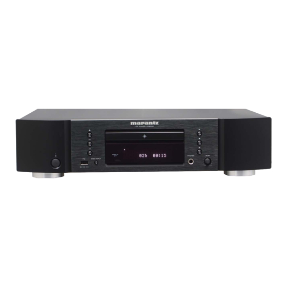
CD Player
CD6006
• For purposes of improvement, specifications and design are subject to change without notice.
• Please use this service manual with referring to the operating instructions without fail.
• Some illustrations using in this service manual are slightly different from the actual set.
Service Manual
Click here!
On-line service parts list
We are getting ready.
On-line owner's manual
http://manuals.marantz.com/CD6006/NA/EN/index.php
http://manuals.marantz.com/CD6006/EU/EN/index.php
http://manuals.marantz.com/CD6006/JP/JA/index.php
CAUTION IN SERVICING
ELECTRICAL
MECHANICAL
REPAIR INFORMATION
UPDATING
Please refer to the MODIFICATION NOTICE.
Ver. 3
Advertisement
Table of Contents

Related Manuals for Marantz CD6006


Summary of Contents for Marantz CD6006
- Page 1 Service Manual Ver. 3 CD Player Click here! CD6006 On-line service parts list We are getting ready. On-line owner’s manual http://manuals.marantz.com/CD6006/NA/EN/index.php http://manuals.marantz.com/CD6006/EU/EN/index.php http://manuals.marantz.com/CD6006/JP/JA/index.php CAUTION IN SERVICING ELECTRICAL MECHANICAL REPAIR INFORMATION UPDATING • For purposes of improvement, specifications and design are subject to change without notice. Please refer to the MODIFICATION NOTICE. • Please use this service manual with referring to the operating instructions without fail. • Some illustrations using in this service manual are slightly different from the actual set.
-
Page 2: Caution In Servicing
CAUTION IN SERVICING SAFETY PRECAUTIONS NOTE FOR SCHEMATIC DIAGRAM NOTE FOR PARTS LIST INSTRUCTIONS FOR HANDLING SEMICONDUCTORS AND OPTICAL UNIT WARNING AND LASER SAFETY INSTRUCTIONS CAUTION IN SERVICING. Initializing This Unit JIG FOR SERVICING... -
Page 3: Safety Precautions
SAFETY PRECAUTIONS ◎ Make a safety check after servicing! The following items should be checked for continued protection of the customer and the service Check that all screws, parts and wires removed or disconnected when servicing have been put back technician. -
Page 4: Instructions For Handling Semiconductors And Optical Unit
NOTE FOR SCHEMATIC DIAGRAM WARNING AND LASER SAFETY INSTRUCTIONS WARNING: WARNING WAARSCHUWING Parts indicated by the z mark have critical characteristics. Use ONLY replacement parts recommended Alle IC’s en vele andere halfgeleiders zijn gevoelig All ICs and many other semi-conductors are voor elektrostatische ontladingen (ESD). -
Page 5: Initializing This Unit
CAUTION IN SERVICING. Initializing This Unit Make sure to initialize this unit after replacing the microcomputer or any peripheral equipment, or the CD PCB. 1. Press the power button to turn off the power. 2. While holding down buttons "PAUSE" and "DISC/INPUT" simultaneously, press the power button to turn on the power. -
Page 6: Schematic Diagrams
ELECTRICAL SCHEMATIC DIAGRAMS SCH01_MAIN_CD_DSP_USB SCH02_MAIN CPU SCH03_AUDIO OUTPUT_POWER SCH04_FRONT_PHONE PRINTED CIRCUIT BOARDS MAIN, MAIN TRANS, HP, FRONT POWER, AUDIO, STBY LED, FLASHER BLOCK DIAGRAM POWER DIAGRAM WIRING DIAGRAM SEMICONDUCTORS 1. IC's 2. FL DISPLAY... - Page 7 SCHEMATIC DIAGRAMS SCH01_MAIN_CD_DSP_USB TO 0A R209 R187 R111 R170 +1.5V_D1 +3.3V_D1 Z101 GND_DA GND_D R142 GND_D Z102 VREF C149 1000P C129 R143 OPEN GND_DA R214 R144 OPEN +3.3V_D2 Z103 R145 OPEN R215 R146 OPEN RFEQO W101 W102 B101 B102 OPEN OPEN C210 CJT1A026...
- Page 8 SCH02_MAIN CPU TO A0 ST+5V S300 JSS2208A Q300 HVTKRA102S 1SS355 D304 GND_D Q301 HVTKRC102S ST+3.3V R309 GND_D * OPTION => MP NOT USE * REMOTE_IN K300 Q302 ST+3.3V CJJ4N102Z KTC3875SYRTK R310 R359 IPO_SDA CN135 CJP09GA193ZY GND_D ST+3.3V GND_D MCU_RESET MCU_RESET [2] JTDO +3.3V_D1 CN2201...
- Page 9 SCH03_AUDIO OUTPUT_POWER AUDIO OUTPUT UNIT +12V 1SS133M 1SS133M ST+10V D3111 D3112 CN3101 Q3303 Q3117 CWB03 KSC1845F KRA104S Q3112 KSC1845F Q3111 KSA992F Q3116 KRC104S R3121 Q3118 Q3106 Q3109 KRC104S +3.3V_D Q3104 KSA992F KSA992F R3106 KSA992F +5V_D Q3101 C3704 OPEN 2SK2145GR Q3301 OPEN R3101 R3105...
- Page 10 SCH04_FRONT_PHONE FCB300 TO MAIN FCC300 TO FCC300 FRONT UNIT FCB300 STBY SW UNIT 16ST103GINK U4003 12 13 14 30 31 32 33 34 35 36 37 38 39 B4001 FST+3.3V C4002 OPEN FDGND C4015 100P C4016 100P FCHGND C4017 100P C4007 FCHGND LDGND2...
-
Page 11: Printed Circuit Boards
PRINTED CIRCUIT BOARDS MAIN, MAIN TRANS, HP, FRONT Lead-free Solder When soldering, use the Lead-free Solder (Sn-Ag-Cu). MAIN (A SIDE) MAIN (B SIDE) MAIN TRANS (A SIDE) MAIN TRANS (B SIDE) Sec. Pri. BN3902 FRONT (A SIDE) FRONT (B SIDE) HP (A SIDE) HP (B SIDE) B4301... - Page 12 POWER, AUDIO, STBY LED, FLASHER POWER (A SIDE) POWER (B SIDE) AUDIO (A SIDE) AUDIO (B SIDE) B3502 BN2101 Z3501 Z4001 J190 Z3912 Z3504 C3542 C3512 C3548 J113 C3921 R3915 D3931 C3926 CN3903 R3912 CN3301 IC3502 J159 D3930 C3547 IC3504 C3544 J105 Q3951...
-
Page 13: Block Diagram
BLOCK DIAGRAM CD6006 BLOCK DIAGRAM +3.3V_D1 +3.3V_D2 +1.5V_D1 VREF +3.3V +5V_D +3.3V_D CD MECHA UNIT +12V -12V +12V -12V KT690EJZ Q311 A/B/C/D/E/F DSP_MCK HDAM-SA2 HDAM LPF IC100 HEX INVERTER FO+/FO- DAC_MCK USB_MCK TR+/TR- ANALOG LCH TC74VHCU04FT SP+/SP- SL+/SL- IC304 LOAD+/LOAD-... -
Page 14: Power Diagram
POWER DIAGRAM CD6006 CURRENT BLOCK DIAGRAM : HEATSINK +3.3V NJM7805 NJM2845 2SD2081 45 mA 0.225 W AUDIO DAC +15V DC15V DC15V HEADPHONE SA2 AMP 30 mA 0.3A 0.3A OP AMP AUDIO DAC 1000 mA 2SB1259 USB Connect 0.225 W 2.004 W 2.004 W... -
Page 15: Wiring Diagram
WIRING DIAGRAM CD6006 WIRING DIAGRAM AC IN AC INLET REMOTE CONTROL DIGITAL AUDIO OUT AUDIO OUT COAXIAL L-CH R-CH OPTICAL POWER PCB K3101 K3201 SUB TRANS CN1101 2.0mm Pitch (A-7) CN3901 3.96mm Pitch *(A) WIRE ASS'Y REF. PART NUMBER COMMENT... - Page 16 SEMICONDUCTORS Only major semiconductors are shown, general semiconductors etc. are omitted to list. The semiconductor which described a detailed drawing in a schematic diagram are omitted to list. 1. IC's MB9AF344NAPMC (IC302) Pin Symbol Pin Name I/O Pu/Pd STBY Description 23 P3E/TIOA4_1 Case of OPEN : "I/O"="O", Output LOW 24 P3F/TIOA5_1...
- Page 17 TC94A92FG (IC100) TC94A92FG (IC17) Pin Symbol Pin Name I/O Pu/Pd STBY Description 73 P21/AN18/SIN0_0/INT06_1/WKUP2 UPDATE_RX MCU uart update rx 74 P20/AN19/INT05_0/CROUT_0/MAD24_1 Case of OPEN : "I/O"="O", Output LOW 75 VSS 76 VCC 77 P00/TRSTX JTRST J-Link emulater 78 P01/TCK/SWCLK JTCK J-Link emulater 79 P02/TDI JTDI...
- Page 18 Symbol Description Default Remarks Symbol Description Default Remarks Focus Error signal / Sub beam add signal FSMoNiT 3AI/F output pin(monitor pin/GND) DVSS3R Grounding pin for 3.3V Muiti-Bit DAC circuit RFZi 3AI/F R channel audio output pin of Audio DAC. RFRP 3AI/F 3AI/F Bulit-in serises R=500...
- Page 19 BA5810FP/FM 光ディスク IC ブロックダイアグラム BA5810 (IC101) Symbol Description Default Remarks VDD3 Power Supply pin for 3.3V Digital circuit CH1~ POWVCC 34 CMOS Port (CH3, CH4) MUTE Schmitt input BUS0 Microprocessor I/F data input/output pin 0 3I/F Refer to [1.2 Pin Assinment Table] CMOS Port 7.5k −...
- Page 20 AK4104 (IC104) UPD63530 (IC105) MCLK BICK CDTO/ SDTI2 SDTI1 AK4104 LRCK TEST4 View TEST3 CCLK TEST2 TEST1 CDTI MCLK Terminal Function µP CCLK Interface Prescaler CDTI CDTO Terminal Function SDTI1 Audio Biphase LRCK Data Encoder Interface BICK Block Diagram MCLK µP CCLK Prescaler...
- Page 21 *For adjustable version only. Figure 1. Typical Application Circ Figure 1. Typical Application Circuit NCP380 (IC106) ILIM* PAD1 ILIM* ILIM* PAD1 FLAG FLAG FLAG TSOP−5 UDFN6 TSOP−6 FLAG FLAG (Top view) Figure 2. Pin Connections TSOP−5 UDFN6 (Top view) *For adjustable version only, otherwise not connected. Figure 2.
- Page 22 CS4398 1. PINOUT DRAWING CS4398 (IC3504) 2. FL DISPLAY DSD_B DSD_A V.F.D (FUTABA, 16ST103GINK) (U4003) DSD_SCLK SDIN SCLK AMUTEC LRCK AOUTA- MCLK AOUTA+ DGND AGND M3 (AD1/CDIN) AOUTB+ M2 (SCL/CCLK) AOUTB- M1 (SDA/CDOUT) BMUTEC M0 (AD0/CS) VREF REF_GND FILT+ PIN CONNECTION CS4398 Terminal Function Pin Name...
- Page 23 MECHANICAL DISASSEMBLY Flowchart 1. TRAY PANEL 2. FRONT PANEL ASSY 3. MECHA ASSY 4. MAIN PCB 5. POWER PCB 6. AUDIO PCB EXPLODED VIEW PACKING VIEW...
- Page 24 DISASSEMBLY Flowchart • Remove each part following the flow below. • Reassemble the removed parts in the reverse order. • Read "SAFETY PRECAUTIONS" before reassembling the removed parts. • If wire bundles are removed or moved during adjustment or part replacement, reshape the wires after completing the work. Failure to shape the wires correctly may cause problems such as noise. •...
-
Page 25: Front Panel Assy
FRONT PANEL ASSY • The photographs with no shooting direction indicated were taken from the top of the unit. (1) Remove the screws. • Photos of CD6006 N1SG are used in this manual. Shooting direction: D View from the bottom... -
Page 26: Mecha Assy
(2) Short the pickup protective solder for the CD mechanism. Then remove the connector and FFC. 3. MECHA ASSY Be sure to wear an earth band. Remove the connector. Proceeding : TOP COVER → TRAY PANEL → FRONT PANEL ASSY → MECHA ASSY (1) Remove the screws. - Page 27 4. MAIN PCB 5. POWER PCB Proceeding : TOP COVER → TRAY PANEL → FRONT PANEL ASSY → MECHA ASSY Proceeding : TOP COVER → POWER PCB (1) Remove the screws. Remove the STYLE PIN and CORD HOLDER. Remove the connector. →...
-
Page 28: Exploded View
EXPLODED VIEW C1-2 C1-7 C1-3 C1-1 C1-5 C1-4 C1-6 WARNING: Parts marked with this symbol z have critical characteristics. Use ONLY replacement parts recommended by the manufacturer. -
Page 29: Packing View
PACKING VIEW UK plug (UK Only) -
Page 30: Repair Information
REPAIR INFORMATION TROUBLE SHOOTING 1. POWER 2. FLD 3. No audio output. MEASURING METHOD AND WAVEFORMS NOTES ON HANDLING AND REPLACEMENT OF THE LASER PICK-UP 1. Protection of the LD 2. Precautions when handling the laser CD mechanism 3. Cautions on assembling and adjustment 4. - Page 31 TROUBLE SHOOTING 1. POWER 1.1. The unit does not power on Replace the fuse. Also, replace Does the ON/STANDBY indicator on the front panel light turn red when the power is turned on? Has the TRANS PCB fuse Is the Main Trans [T3951] pri- the main trans [T3951] if there blown? mary side winding wire on the...
- Page 32 2. FLD 2.1. FLD is not lit Are the MAIN PCB resistance Is the VP output voltage Is the transistor collector input Check the transistor [Q3901] Is the MAIN PCB filament out- [R308] and POWER PCB resis- Check the condition of the (+25V) for the MAIN PCB nor- voltage (+49V) for the POWER and the solder of circuits that...
- Page 33 2.2. FLD control waveform DIS_CD DIS_SCL(CP) DIS_SO(DA) 2.3. Remote control signals are not being received. Is the power supply voltage (FST+3.3V) of the Check the input voltage of [U3904] on the remote control sensor [U4001] on the FRONT POWER PCB, as well as the circuits and solder of PCB normal? any circuits that carry this output load.
-
Page 34: No Audio Output
3. No audio output. 3.1. No sound is output when a CD is played back. Is the solder of the [IC3504] (DAC) on the AUDIO Check Soldering or replace for the following PCB normal? parts. Check Soldering or replace for the following Is the power supply voltage for the CD normal? parts. - Page 35 3.1. No sound is output when a USB, iPod is played back. Is the digital signal to the DAC IC on the MAIN Check the IC below the MAIN PCB as well as the Is the MAIN PCB connector disconnected? PCB normal? Connect the connectors correctly.
- Page 36 3.4. USB DSP communication waveforms 3.5. USB for data waveform DP (D+) USB_RTS USB_CTS DM (D-) USB_SO USB_SI...
-
Page 37: Measuring Method And Waveforms
MEASURING METHOD AND WAVEFORMS Measuring Disc : 4822 397 30184 TCD-784 (It is recommended to use extension wires between the probe and test points.) MAIN PCB : test point RFEQO LOAD+ USB SO LOAD- DIS CD USB SI FSMONIT DIS SCL(CP) DIS SO(DA) MCLK DATA... - Page 38 WAVEFORMS 1. DISC PLAY RF WAVEFORM(EYE-PATTERN) 2. DISC DETECTION 3. TOC READ 4. FOCUS ADJUSTMENT 1.1 CD(TCD-784)Play 2.1 CD(TCD-784)DISC DETECTION 3.1 CD(TCD-784)TOC READ 4.1 CD(TCD-784)FOCUS ADJUSTMENT ②RFO ②RFO ③FSMONIT 200mV 200mV ③FSMONIT ④FOO ④FOO ①RFEQO ⑤TEI 500Mv ⑤TEI 500Mv ⑥ TRO ⑥...
-
Page 39: Protection Of The Ld
NOTES ON HANDLING AND REPLACEMENT OF THE LASER PICK-UP 1. Protection of the LD Solder a part of the LD circuit to short-circuit. After connecting the circuit, remove the soldering form. Precautions when handling the laser CD mechanism 2. Precautions when handling the laser CD mechanism •... -
Page 40: Special Mode Setting Button
SPECIAL MODE Special mode setting button b No. 1 - 7 : While holding down buttons "A" and "B" simultaneously, insert the AC plug into the wall outlet to turn on the power. Mode Button A Button B Descriptions The firmware version is shown on the display. Errors that have occurred are displayed. Version Display Mode DISC/INPUT PLAY... -
Page 41: Version Display Mode
1. Version Display Mode 2. Display check mode 1.1. Actions While holding down buttons the "DISC/INPUT" and " 2 " buttons simultaneously, insert the AC plug to turn the power on. Version information is displayed when the device is started in this mode. This mode is cancelled when the power is turned off. -
Page 42: Cd Test Mode
4.2. Servo check 4. CD test mode • Press " 1 " button. Execute the following steps. While holding down buttons the " 8 / 6 " and " 1 " buttons simultaneously, insert the AC plug to turn (1) LD ON(while servo is stopped) the power on. - Page 43 4.3. Pickup movement (4) TRACKING GAIN • If button " 8 / 6 " or " 7 / 9 " is pressed in the stopped state, the pickup moves in the REV (inner circumference) or FWD (outer circumference) direction. X X X X •...
- Page 44 5.2. Chucking mode 5. CD Heat run mode Press the " 2 " button while stopped after CD heat run mode has started and TOC reading has been com- • Insert a disc and press the " 8 / 6 " and " 2 " buttons together while inserting the AC plug and turn- pleted.
-
Page 45: Error Display
5.3. Error display 6. Accumulated laser on time display mode E1-00 : Disc cannot be detected. While holding down buttons the " 8 / 6 " and " 3 " buttons simultaneously, insert the AC plug to turn E1-01 : Tracking offset adjustment not possible. the power on. - Page 46 UPDATING PROCEDURE AFTER REPLACING THE U-COM, ETC. FIRMWARE UPDATE PROCEDURE 1. Items necessary for update 2. Updating via System u-com (IC302) 3. Updating via USB-A (IC107)
- Page 47 PROCEDURE AFTER REPLACING THE U-COM, ETC. The procedure after replacing the u-COM (microprocessor), flash ROM, etc. is as follows. Procedure PCB Name Ref. No. Description Remark after Re- placement MAIN IC302 MB9AF344NAPMC SOFTWARE : System MAIN IC107 I.C , SERIAL FLASH(8M) SOFTWARE : USB-A Procedure after Replacement A : The software has been written.
-
Page 48: Firmware Update Procedure
FIRMWARE UPDATE PROCEDURE 1. Items necessary for update Items necessary for update are as follows. Offered / not Offered Update Type Needed Part for Update Requirement Standard Service Equipment Purchase from D&M Article code Download from SDI Not offered by D&M RS-232C cable 9P (Male), Straight 8U-210100S WRITING KIT... -
Page 49: Items To Be Prepared
2. Updating via System u-com (IC302) 1. Items to Be Prepared 3. Installing the Software Install the writing software "FUJITSU FLASH MCU Programmer for FM3/FM4" on your computer. (1) Obtain "pcwfm3-v01l07.zip" from SDI. (2) Personal Computer (Be installed "FUJITSU FLASH MCU Programmer for FM3/FM4"). (3) RS-232C cable (9P (Male), Straight). - Page 50 4. Run the FLASH MCU Programmer (5) The following display appears when the firmware update is complete. Click "OK". (1) Press the power button to turn on the power. (2) Execute "FUJITSU FLASH MCU Programmer for FM3/FM4" after installing it on your computer. Double-click FLASH MCU Programmer to launch FLASH MCU Programmer Start.
- Page 51 • If a USB memory device cannot be updated, replace it with a different USB memory device and per- form the update again. 3.2. Unzipping the Downloaded File Unzip the downloaded file on your computer. CD6006 USB_CD6006_XXXX.zip copy to USB flash drive The "DCD1650U.BIN" file is created upon unzipping the file.
-
Page 52: Start The Update
3.4. Start the update. 3.6. Error display While holding down buttons the " 7 / 9 " and " 2 " buttons simultaneously, insert the AC plug to turn (1) If the update file name is incorrect the power on. 3.5. - Page 53 Copyright 2016 D&M Holdings Inc. All rights reserved.
- Page 54 FR PW AD FR PW AD PCB ASS'Y ※Parts indicated by "nsp"on this table cannot be supplied. Part indicated by "@" mark is not illustrated in the exploded view ※The parts listed below are only for maintenance. Therefore they might differ from the parts used in the unit in appearances or dimensions NOTE:The symbols in the column Remarks indicate the following destinations.
- Page 55 FR PW AD REF No. Part No. Part Name Remarks Q'ty New Ver Q3951-3 SCREW CTB3+8FFB Q3951-4 943219500190M T.R, 2SD2081, NPN, TO220F, SANKEN CVT2SD2081 Q3951-5 COMPOUND , SILICONE K8AYG6260 Q3952-1 HEAT SINK ASS'Y(CVT2SB1259+CMY1A338) CVT2SB1259BSA Q3952-2 HEAT SINK 25MM CMY1A338 Q3952-3 943219500170M T.R, 2SB1259, PNP, TO220F, SANKEN CVT2SB1259...
- Page 56 FR PW AD REF No. Part No. Part Name Remarks Q'ty New Ver R3404 RES, CARBON(1/5W,56ohm,J) CRD20TJ560T R3405 RES, CARBON(1/5W,6.8Kohm,J) CRD20TJ682T R3406 RES, CARBON(1/5W,33ohm,J) CRD20TJ330T R3408 RES, CARBON(1/5W,33ohm,J) CRD20TJ330T R3503 RES, CHIP(1608/5%/0ohm) CRJ10DJ0R0T R3504 RES, CHIP(1608/5%/0ohm) CRJ10DJ0R0T R3573 RES, CHIP(1608/5%/0ohm) CRJ10DJ0R0T R3579 RES, CHIP(1608/5%/0ohm)
- Page 57 FR PW AD REF No. Part No. Part Name Remarks Q'ty New Ver C3204 943133501570M CAP , POLYPROPYLENE(FAS(133)-200V-181K) CCMP2B181KS17T C3205 943133501570M CAP , POLYPROPYLENE(FAS(133)-200V-181K) CCMP2B181KS17T C3206 943133501580M CAP , POLYPROPYLENE(FAS(133)-200V-221K) CCMP2B221KS17T C3208 943133501590M CAP , POLYPROPYLENE (FAS(133)-200VDC 470KTP CCMP2B470KS17T C3209 00MOA227025R0 CAP, ELECT(220UF/25V, 10X20, ELNA/ROA) CCEA1EROA221T C3210...
- Page 58 FR PW AD REF No. Part No. Part Name Remarks Q'ty New Ver B4301 WIRE ASS'Y CWE8202150RV BK10 BRACKET , PCB CMD1A569-V1 BK11 BRACKET , PCB CMD1A569-V1 BK12 BRACKET , PCB CMD1A569-V1 BK13 BRACKET , PCB CMD1A569-V1 BK41 EARTH PLATE (HP) VMC1A491 BN1101 USB WIRE ASS'Y (5PIN,350MM,61205032500AS)
- Page 59 MAIN MAIN PCB ASS'Y ※Parts indicated by "nsp"on this table cannot be supplied. Part indicated by "@" mark is not illustrated in the exploded view ※The parts listed below are only for maintenance. Therefore they might differ from the parts used in the unit in appearances or dimensions NOTE:The symbols in the column Remarks indicate the following destinations.
- Page 60 MAIN REF No. Part No. Part Name Remarks Q'ty New Ver R194 RES, CHIP(1608/5%/10Kohm) CRJ10DJ103T R195 RES, CHIP(1608/5%/10Kohm) CRJ10DJ103T R196 RES, CHIP(1608/5%/10Kohm) CRJ10DJ103T R197 RES, CHIP(1608/5%/10Kohm) CRJ10DJ103T R198 RES, CHIP(1608/5%/33ohm) CRJ10DJ330T R199 RES, CHIP(1608/5%/33ohm) CRJ10DJ330T R200 RES, CHIP(1608/5%/33ohm) CRJ10DJ330T R201 RES, CHIP(1608/5%/33ohm) CRJ10DJ330T R202...
- Page 61 MAIN REF No. Part No. Part Name Remarks Q'ty New Ver R381 RES, CHIP(1608/5%/0ohm) CRJ10DJ0R0T R382 RES, CHIP(1608/5%/0ohm) CRJ10DJ0R0T R383 RES, CHIP(1608/5%/0ohm) CRJ10DJ0R0T R384 RES, CHIP(1608/5%/0ohm) CRJ10DJ0R0T R385 RES, CHIP(1608/5%/0ohm) CRJ10DJ0R0T R386 RES, CHIP(1608/5%/0ohm) CRJ10DJ0R0T R387 RES, CHIP(1608/5%/0ohm) CRJ10DJ0R0T R388 RES, CHIP(1608/5%/0ohm) CRJ10DJ0R0T R389...
- Page 62 MAIN REF No. Part No. Part Name Remarks Q'ty New Ver C306 CAP, CHIP(1608, 50V/0.1uF) CCUS1H104KC C307 CAP, CHIP(1608, 50V/0.1uF) CCUS1H104KC C308 CAP, CHIP(1608, 50V/0.1uF) CCUS1H104KC C309 00MOA107025Z1 CAP , ELECT (ELNA/R0S, 25V/100UF) HCEA1ER101T C310 CAP, CHIP(1608, 50V/0.1uF) CCUS1H104KC C311 CAP, CHIP(1608, 50V/0.1uF) CCUS1H104KC C312...
- Page 63 CD MECHANISM (Traverse) CJD5C6Z01Z C4-2 30201005100AD LM BELT CDV1A011 LOADING MECHA ! C5 00MYJ04002640 AC INNET ASS'Y CJJ8A006ZW 421410006004M BADGE , MARANTZ CGB1A206 943415100410M ORNAMENT, DOOR BLACK CGR1A552ZB37 943415100400M ORNAMENT, DOOR CGR1A552RMZD10 943416101150M WINDOW , FIP CGU1A423A12Y PANEL , SUB CD5003/N1B...
- Page 64 CJA2N075Z ! 5 611050028007S CORD , POWER JPN INLET TYPE (250V) CJA2J115ZV BAG , POLY VPB1A008Z 30701022500AS REMOCON TRANSMITER ASS'Y (PM6006&CD6006) CARTPMCD6006 LABEL , CONTROL VQB2A993Z LABEL , BAR CODE(SET) VQB1A978 LABEL , CONTROL VQB2A993Z BATTERY , AAA 2PCS IN PACK...
Need help?
Do you have a question about the CD6006 and is the answer not in the manual?
Questions and answers