Table of Contents
Advertisement
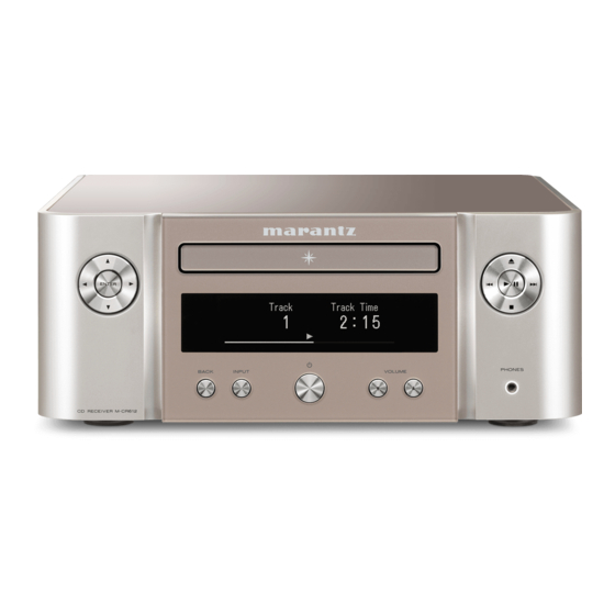
NETWORK CD RECEIVER
M-CR612
• For purposes of improvement, specifications and design are subject to change without notice.
• Please use this service manual when referring to the operating instructions without fail.
• Some illustrations used in this service manual are slightly different from the actual product.
Service Manual
Click here!
On-line service parts list
http://dmedia.dmglobal.com/Document/DocumentDetails/25651
ONLINE PARTS LIST
(P5)
WEB owner's manual
NA:
http://manuals.marantz.com/MCR612/NA/EN/index.php
EU:
http://manuals.marantz.com/MCR612/EU/EN/index.php
AP:
http://manuals.marantz.com/MCR612/AP/ZH/index.php
JP:
http://manuals.marantz.com/MCR612/JP/JA/index.php
Upload is planned for the time of a future press release.
BEFORE SERVICING THIS UNIT
ELECTRICAL
MECHANICAL
REPAIR INFORMATION
UPDATING
Please refer to the MODIFICATION NOTICE.
Confidential
Ver. 2
Advertisement
Table of Contents

Related Manuals for Marantz M-CR612


Summary of Contents for Marantz M-CR612
- Page 1 Service Manual Ver. 2 NETWORK CD RECEIVER M-CR612 Click here! On-line service parts list http://dmedia.dmglobal.com/Document/DocumentDetails/25651 ONLINE PARTS LIST (P5) WEB owner’s manual http://manuals.marantz.com/MCR612/NA/EN/index.php http://manuals.marantz.com/MCR612/EU/EN/index.php http://manuals.marantz.com/MCR612/AP/ZH/index.php http://manuals.marantz.com/MCR612/JP/JA/index.php Upload is planned for the time of a future press release. BEFORE SERVICING THIS UNIT...
- Page 2 BEFORE SERVICING THIS UNIT SAFETY PRECAUTIONS NOTE FOR SCHEMATIC DIAGRAM HANDLING THE SEMICONDUCTOR AND OPTICS WARNING AND LASER SAFETY INSTRUCTIONS ONLINE PARTS LIST Accessing the Parts List Searching Part Numbers or Ref. Numbers NOTE FOR PARTS LIST SERIAL NUMBER Serial Number Organization SKU Code of this Unit POST-SERVICE PRECAUTIONS Initializing this Unit...
-
Page 3: Safety Precautions
SAFETY PRECAUTIONS The following items should be checked for continued protection of the customer and the service technician. Leakage current check Before returning the set to the customer, be sure to carry out either (1) a leakage current check or (2) a line to chassis resistance check. If the leakage current exceeds 0.5 milliamps, or if the resistance from chassis to either side of the power cord is less than 460 kohms, the set is defective. -
Page 4: Note For Schematic Diagram
NOTE FOR SCHEMATIC DIAGRAM WARNING AND LASER SAFETY INSTRUCTIONS WARNING: WARNING WAARSCHUWING Parts indicated by the z mark have critical characteristics. Use ONLY replacement parts recommended Alle IC’s en vele andere halfgeleiders zijn gevoelig All ICs and many other semi-conductors are voor elektrostatische ontladingen (ESD). -
Page 5: Note For Parts List
On-line service parts list http://dmedia.dmglobal.com/Document/DocumentDetails/XXXXX ONLINE PARTS LIST (P5) WEB owner’s manual http://manuals.marantz.com/AAAAA/NA/EN/index.php http://manuals.marantz.com/AAAAA/EU/EN/index.php http://manuals.marantz.com/AAAAA/AP/ZH/index.php Upload is planned for the time of a future press release. BEFORE SERVICING THIS UNIT NOTE : If the web browser does not open automatically, copy the URL and paste it into the address bar (3) Next, click the "Sheet"... - Page 6 SERIAL NUMBER Serial Number Organization The 14-digit serial number that contains the code of the manufacturing plant and the manufacturing date. 14 digits Factory Manufactured Cumulative Year, month code code serial number The last Month 2digit of year (01 ~ 12) SKU Code of this Unit Product SKU SKU Code...
-
Page 7: Initializing This Unit
POST-SERVICE PRECAUTIONS Initializing this Unit Make sure to initialize this unit after replacing the microcomputer or any peripheral equipment, or the PCB. 1. Press the power operation button to turn off the power, and remove the AC plug from the socket. Insert the AC plug while pressing buttons "INPUT"... -
Page 8: Schematic Diagrams
ELECTRICAL SCHEMATIC DIAGRAMS SCH01 MAIN STA309, TAS5558 SCH02 MAIN MICOM SCH03 MAIN DIR SCH04 MAIN PBTL SCH05 NETWORK LEGO SCH06 FRONT SCH07 AMP SCH08 INPUT SCH09 KEY, HP, DAB, OPT SCH10 CD SCH11 SMPS PRINTED CIRCUIT BOARDS MAIN, PBTL, NETWORK INPUT, AMP, LED_L, LED_R, FRONT, KEY_L, KEY_R, OPT, DAB, CD BLOCK DIAGRAM POWER DIAGRAM... - Page 9 SCHEMATIC DIAGRAMS SCH01 MAIN STA309, TAS5558 RLY_GND RLY_GND RLY_+12V RLY_+12V AGND AGND A_+12V A_+12V A_-12V A_-12V C101 220/10 DGND C102 100N-16V +3.3VD 309_+3V3 C105 BD121 +5V_D 100N-16V L101 ST+5V STA309_PDN C104 +3.3V_CPU 100N-16V D_+12V +29V R103 R104 R105 8K2-F C108 C109 MCR612 PWM PART HP_L...
- Page 10 SCH02 MAIN MICOM CP120 TO CP1003 TO 2A TO A0 MCR612 MICOM PART LEGO PCB DIR PART PWM PART CP101 C240 CONTROL ANALOG ANALOG SPDIF CONTROL 1N-50V C241 H/P_R 10N-50V C242 H/P_GND DGND AGND 100N-16V H/P_L TO CN801 AIOS4_SDOUT_I2S_0 AIOS4_SCLK_I2S_0 AIOS4_LRCK_I2S_0 AIOS4_MCLK0 CP102...
- Page 11 SCH03 MAIN DIR MCR612 DIR PART PACKAGE CHANGED +3.3VD R406 CD_SPDIF_1 R407 R408 DGND +3.3VD R409 OPT_1_OUT R410 R429 DGND +3.3VD +3.3VD R432 DIR1 OPT_2_OUT R435 R438 DGND DAB ONLY(N1B/N1SG) CD_SPDIF SPDIF OPT1_SPDIF +3.3VD OPT2_SPDIF R448 DAB_SPDIF A_+5V R449 R450 DGND DGND +3.3VD...
- Page 12 SCH04 MAIN PBTL MCR612 RELAY MCR612 PBTL_RELAY PART PF61 RLY_GND RLY_GND PBTL_RLON RLY_+12V PF61 TO _PF102 RLY_12V1 0-3216 RLY61 JZC-42F RLY_12V1 0-3216 RLY62 JZC-42F PF62 KRC105S KRC105S PBTL_RLON_1 RLY_GND1 TO _PF101 PF62 GND LINE POWER+ LINE POWER- LINE ANALOG AUDIO DIGITAL AUDIO PWM SIGNAL...
- Page 13 SCH05 NETWORK LEGO NETWORK U1001 TPS22975 L1001 CB05YTYH221-2012 LEGO5V P5V_NET VOUT LEGO5V GND_D VOUT VBIAS R1001 0-1005 GND_D GND_D U1002 TPS22975 L1002 CB05YTYH221-2012 NET3.3V VOUT NET3.3V VOUT VBIAS R1002 0-1005 CP1003 GND_D GND_D DIR_LRCK NET3V3_POWER C1009 100N-16V-1005 DIR_BCK NET5V_POWER DIR_DATA C1010 100N-16V-1005 NET_FACT_RST...
- Page 14 SCH06 FRONT MCR612 FRONT _FPC1 MAIN B`D TO FPC101 FPC1 0.5-11-33P DGND +3V3_CPU LED_GREEN LED_RED POWR LED STATUS LED_OR LED_R LED_G LED_OR DGND H/P_DET GREEN LED_5V ORANGE KEY2 NOTHING KEY3 KRC102S KRC102S KEY1 KEY1 DGND 180828 Changed value of R7 from 270ohm to 560ohm _CN2 100N-50V...
- Page 15 SCH07 AMP MCR612 AMP SU AUDIO PART CO.15 100/16(PX) C596 +12V_5142 ADGND 180831 C590 10000N/25V 100/16 -> 220/25(RJH) BD120 BD120 Point B C594 L514 L515 10000N/25V R586 R587 R588 C595 SU AUDIO PART CO.17 100N SHINYEI SU AUDIO PART CO.18 C588 R585 GVDD_C...
- Page 16 SCH08 INPUT MCR612 INPUT 180621 Added 0-3216 CP901 CP901 C125Z1-09 D901 DAB_DI 180619 TU_RST/DAB_DI Changed value DAB_DO TU_INT/DAB_DO 220N -> 100N +7.5V IC901 KIA7808API TUNER_DAB_ON D906 1N4007 R901 TUNER_DAB_ON +12V D+5V D+5V NET00072 SPDIF DAB_SPDIF TO CP803 CP902 CP902 C125Z1-05 OPT_OUT2 OPT2 OPT_OUT1...
- Page 17 SCH09 KEY, HP, DAB, OPT MCR612 KEY/HP/DAB/OPT B'D DAB B'D CP801 KEY_L B`D ADC3 ADC2 ADC1 R801 CP803 J807 R834 ADC0 R802 J804 C801 R833 COSMOS BD TO BD AUDIO_L C802 CP803 CP802 R804 AGND C804 AUDIO_R C803 SCL0 DAB_DI R803 SDA0 DAB_DO...
- Page 18 SCH10 CD MCR612 CD TO CD Pick-up CN701 C701 10N-50V C702 100N-50V KTA1504S C703 470/10V C776 100N-50V Q701 R702 L701 BRL3225T100K C783 100N-50V R703 GND_DRV C817 10N-50V R704 C704 100N-50V C706 1000P-50V R705 C705 470/10V C707 100N-50V GND_DRV C708 10N-50V D706 1SS355 C818...
- Page 19 SCH11 SMPS L411 L411 5.6uH (BAR) 5.6uH (BAR) CN411 T821 T821 D411 D411 +29V CN411 CN411 +29V#1 DC_LINK PQ3225 PQ3225 SDB10200PI SDB10200PI L413 L413 L412 L412 YMW025-06 YMW025-06 5.6uH (BAR) 5.6uH (BAR) 5.6uH (BAR) 5.6uH (BAR) +29V#2 +29V#1 C805 C805 C806 C806 B821...
-
Page 20: Printed Circuit Boards
PRINTED CIRCUIT BOARDS MAIN, PBTL, NETWORK Lead-free Solder When soldering, use the Lead-free Solder (Sn-Ag-Cu). MAIN (A SIDE) MAIN (B SIDE) NETWORK (A SIDE) NETWORK (B SIDE) R1152 R1143 R1153 R1149 C1032 L1007 Lch+ (RED) (BK) Lch- Rch- (BK) (RED) Rch+ C1023 C1022... - Page 21 INPUT, AMP, LED_L, LED_R, FRONT, KEY_L, KEY_R, OPT, DAB, CD INPUT (A SIDE) INPUT (B SIDE) FRONT (A SIDE) FRONT (B SIDE) KEY L (A SIDE) KEY L (B SIDE) OPT (A SIDE) OPT (B SIDE) C831 5.+3V3 C833 J801 4.DGND C832 5.+3V3...
-
Page 22: Block Diagram
BLOCK DIAGRAM FRONT LED B'D FRONT B'D SWITCHED-MODE POWER SUPPLY SMD type LED (2.8x3.2mm) Transformer 1 White, Blue, Green, Orange White, Blue, Green, Orange Switch Status LED [MCR612] (uCOM, NET) (EU ver White Only) Cursor Up Cursor Down Cursor Right Cursor Left OLED Enter... -
Page 23: Power Diagram
POWER DIAGRAM M-CR612 POWER Supply Diagram +29V +29V D-amp TAS5142 SMPS Trans SUB POWER CONT (Power-H) IC221SN7812 +12V_D +12V D-amp Regulator TAS5142 IC705 KIA7808AF +8V_M Regulator BA5810 Driver IC222 SN7812 +12V_A +12V +12V H/P&SW &Preout Regulator OPAMP,Mute +12V Relay IC901 KIA7808 +7.5V... -
Page 24: Wiring Diagram
WIRING DIAGRAM M-CR612 WIRE BLOCK DIAGRAM AC INLET 14P PIN SOCKET 10P PIN SOCKET PBTL RELAY OPTICAL INPUT / CNT (ONLY EU) 18P PIN SOCKET Verona2 26P B`D TO B`D MAIN TRANS 26P B`D TO B`D 31P BD TO BD... - Page 25 SEMICONDUCTORS Only major semiconductors are shown, general semiconductors etc. are omitted to list. The semiconductor which described a detailed drawing in a schematic diagram are omitted to list. 1. IC's R5F56108VNFP (MAIN : IC111) Hardware Port Name Function Name Detail of Function PD/PU E20 Emulator control pin/When normal operating mode,set to TRST#/P34/IRQ4...
- Page 26 Hardware Hardware Port Name Function Name Port Name Function Name Detail of Function Detail of Function PD/PU PD/PU P80/SCK10 DIR2_DO DIR PCM9211(Distribution) Control 117 P60 CD_SBSY 10K PU CD Monitor 3 (default : Output) DIR2_DI DIR PCM9211(Distribution) Control 118 VCC Power Supply Pin PC3/TXD5 /5558_PDN...
- Page 27 Pin Layout (Top View) TC94A92FG (CD : IC701) Terminal Function Symbol Description Default Remarks DSP VCO - EFM and PLCK Phase difference VCoi signal output pin. 3 state output 3AI/F (DSP VCO control voltage inputr pin.) VDD3 CDMoN3 BUS0 Pio14/CDMoN2 CD-DSP-Power supply for 3.3V RF BUS1 Pio13/CDMoN1...
- Page 28 Default Remarks Default Remarks Symbol Description Symbol Description CMOS Port Disc servo equalizer output pin Bulit-in output R=3.3 k Ω 3AI/F Pio7 Port 7(General Input/Output Port ) Schmitt input 3I/F Refer to [1.2 Pin Assinment Table] Power supply pin for 1.5V Decoder-DSP VDD1-3 3I/F /CD circuit...
- Page 29 PCM9211 BA5810FP/FM www.ti.com SBAS495 – JUNE 2010 PIN CONFIGURATIONS 光ディスク IC BA5810 (CD: IC701) PCM9211 (MAIN : IC117/IC120) PT PACKAGE LQFP-48 (TOP VIEW) ブロックダイアグラム CH1~ POWVCC 34 (CH3, CH4) ERROR/INT0 VDDRX MUTE NPCM/INT1 RXIN1 7.5k MPIO_A0 − − LEVEL MPIO_A1 RXIN2 7.5k SHIFT...
- Page 30 NJU72751A NJU72751A (INPUT : IC901) PCM9211 Pin Descriptions DESCRIPTION PIN CONFIGURATION NAME TOLERANT ERROR/INT0 DIR Error detection output / Interrupt0 output NPCM/INT1 DIR Non-PCM detection output / Interrupt1 output MPIO_A0 Multipurpose I/O, Group A(1) MPIO_A1 Multipurpose I/O, Group A(1) MPIO_A2 Multipurpose I/O, Group A(1) MPIO_A3 Multipurpose I/O, Group A(1)
- Page 31 • 36-pin PSOP3 package (DKD) TAS5142 • 44-pin HTSSOP PowerPad™ package (DDV) Both package types contain a heat slug that is located on the top side of the device for convenient thermal www.ti.com coupling to the heatsink. SLES126B – DECEMBER 2004 – REVISED MAY 2005 TAS5142DKD (AMP : IC500, IC502) TAS5142 Block Diagram DKD PACKAGE...
- Page 32 These devices have limited built-in ESD protection. The leads should be shorted together or the device placed in conductive foam during storage or handling to prevent electrostatic damage to the MOS gates. TAS5558 (MAIN : IC104) TAS5558 Block Diagram Block Diagram Fixed Flow SDIN1 Serial Audio...
- Page 33 Pin connections PCM5100A, PCM5101A, PCM5102A PCM5100A-Q1, PCM5101A-Q1, PCM5102A-Q1 PCM5100APWR (MAIN: IC39) STA309A_ST (MAIN : IC101) Figure 3. Pin connection (top view) www.ti.com SLAS859C – MAY 2012 – REVISED MAY 2015 7 Pin Configuration and Functions 59 58 57 56 53 52 51 50 49 PW 20-Pin Package OUT2_A (Top View)
- Page 34 Type Name Description 3.3-V capable TTL 16mA output buffer OUT2B PWM channel 2 output B 3.3-V capable TTL 16mA output buffer OUT2A PWM channel 2 output A 3.3-V capable TTL 16mA output buffer OUT1B PWM channel 1 output B 3.3-V capable TTL 16mA output buffer OUT1A PWM channel 1 output A 3.3-V capable TTL 4mA output buffer...
- Page 35 2. FL DISPLAY MXS4035A MXS4035A IO Interfaces...
- Page 36 3. Remote Code Table Extended Code M-CR612 must receive following codes. These codes are not included in the RC014CR RC014CR RC-5/RC-5 Ext. RC-5/RC-5 Ext. KEY No. Key Name System Command Extension Name System Command Extension OPEN/CLOSE Power on SLEEP Power off...
- Page 37 MECHANICAL DISASSEMBLY Flowchart 1. TOP PANEL 2. FRONT PANEL ASSY 3. CD MECHA ASSY 4. MECHA SUPPORT L/R 5. SHIELD COVER 6. SMPS PCB 7. BACK CHASSIS ASSY 8. NETWORK ASSY 9. INPUT ASSY 10. AMP and PBTL PCB 11. MAIN PCB EXPLODED VIEW OF CD MECHANISM UNIT POINTS OF GREASING EXPLODED VIEW...
- Page 38 DISASSEMBLY Flowchart • Remove each part following the flow below. • Reassemble the removed parts in the reverse order. • Read "SAFETY PRECAUTIONS" before reassembling the removed parts. • If wire bundles are removed or moved during adjustment or part replacement, reshape the wires after completing the work. Failure to shape the wires correctly may cause problems such as noise. • See "EXPLODED VIEW" PANEL SIDE TOP PANEL MECHA SUPPORT L/R DISASSEMBLY DISASSEMBLY 1. TOP PANEL 4. MECHA SUPPORT L/R and "EXPLODED VIEW" and "EXPLODED VIEW" TOP PANEL MECHA SUPPORT L/R Ref. No. of EXPLODED VIEW : 30 Ref. No. of EXPLODED VIEW : 31,33 FRONT PANEL ASSY SHIELD COVER INPUT ASSY DISASSEMBLY DISASSEMBLY DISASSEMBLY 2. FRONT PANEL ASSY 5. SHIELD COVER 9. INPUT ASSY and "EXPLODED VIEW" and "EXPLODED VIEW" and "EXPLODED VIEW"...
-
Page 39: Front Panel Assy
Proceeding : PANEL SIDE → TOP PANEL → FRONT PANEL ASSY • The photographs with no shooting direction indicated were taken from the top of the unit. (1) Open the CD tray and remove WINDOWS LOADER. • Photos of M-CR612 U1B are used in this manual. View from the bottom The viewpoint of each photograph (Shooting direction : X) [View from the top] ↓Shooting direction: B↓ View from the CD MECHA bottom (2) Remove the screws. View from the bottom ↑Shooting direction: A↑... -
Page 40: Shield Cover
(3) Remove the connector. 3. CD MECHA ASSY CD PCB Proceeding : PANEL SIDE → TOP PANEL → FRONT PANEL ASSY → CD MECHA ASSY (1) Remove the screws. Remove the connector and FFC. CN701 CN704 CN701 CN705 CN702 4. MECHA SUPPORT L/R Proceeding : PANEL SIDE → TOP PANEL FRONT PANEL ASSY →... -
Page 41: Network Assy
8. NETWORK ASSY 6. SMPS PCB Proceeding : PANEL SIDE → TOP PANEL → FRONT PANEL ASSY → CD MECHA ASSY Proceeding : PANEL SIDE → TOP PANEL → FRONT PANEL ASSY → CD MECHA ASSY → MECHA SUPPORT L/R → SHIELD COVER → BACK CHASSIS ASSY →... - Page 42 10. AMP and PBTL PCB Proceeding : PANEL SIDE → TOP PANEL → FRONT PANEL ASSY → CD MECHA ASSY → MECHA SUPPORT L/R → SHIELD COVER → BACK CHASSIS ASSY → NETWORK ASSY → INPUT ASSY → AMP and PBTL PCB (1) Remove the screws. Remove the connector.
-
Page 43: Exploded View Of Cd Mechanism Unit
EXPLODED VIEW OF CD MECHANISM UNIT http://dmedia.dmglobal.com/Document/DocumentDetails/25651 Parts List :... -
Page 44: Points Of Greasing
POINTS OF GREASING FRAME MAIN TRAY DISC GEAR TRAY SLIDER CAM Point to apply EM30L (NO.1‐NO.6) Point to apply EM30L (9 in total) Point to apply EM30L (2 in total) Point to apply EM30L (5 in total) Point to apply EM30L (NO.7‐NO.13) Oiling position Dosage Oiling position... -
Page 45: Exploded View
EXPLODED VIEW http://dmedia.dmglobal.com/Document/DocumentDetails/25651 Parts List : S2x2 S9x2 S2x2 S10x2 S2x1 S2x4 S8x2 S11x1 A-64 S3x3 S5x4(U1,F,K1) S5x2(N1) A-25 S4x9 S7x3 S6x2 S1x1 (onli N1) S13x2 S2x1 S3x2 S1x3 The following serial numbers use cushion. •MCR612U1B----from BGU36200201001 •MCR612N1B----from BGW36191110381 S1x4 •MCR612N1SG--from BGV36191104801 •MCR612K1SG--from BGT36191100301 •MCR612FB-----from BGX36191102051... - Page 46 PACKAGING VIEW http://dmedia.dmglobal.com/Document/DocumentDetails/25651 Parts List : UK plug (UK Only) MANUAL ASSY(K1SG) MANUAL ASSY(FN/FB) 61 2 M CR MANUAL ASSY(U1B) * BOX BOTTOM TAPE( O ) MANUAL ASSY(N1B/N1SG)
-
Page 47: Repair Information
REPAIR INFORMATION TROUBLE SHOOTING SPECIAL MODE 1. This unit does not start, not LED lighting. Special mode setting button 2. No Sound. Noise generated 1. Selecting the Mode 1 for Service-related 1-1. Version Display Mode MEASURING METHOD AND WAVEFORMS 1-2. Product mode 1-3. -
Page 48: No Sound. Noise Generated
TROUBLE SHOOTING 1. This unit does not start, not LED lighting. 2. No Sound. Noise generated 2.1. COMMON Check Power Supply Voltages for SMPS. • CN221 : 11pin +3.3V (PP) Pulse signal of 50 Hz or 60 Hz Replace the SMPS. •... - Page 49 2.2. CD 2.4. TUNER (U / F / K Only) Check Power Supply Voltages. Check Power Supply Voltages. CD PCB INPUT PCB Replace defective parts. • CN703 : 4pin +12V_D • PACK901 : 3 pin TU_5V • IC705 OUT : +8V Replace defective parts.
-
Page 50: Digital-In
2.5. Analog In 2.7. USB / ETHERNET / Wi-Fi Check Power Supply Voltages for Network LEGO module. Check the analog audio signal. Replace defective parts. Network PCB Replace defective parts. • JK902 : L, R • CP1003 : 27,28,29pin : NET_5V Replace the SMPS. - Page 51 2.8. ANALOG AUDIO OUT 2.9. Headphone OUT Check Power Supply Voltages. Check Power Supply Voltages. Replace defective parts. Replace defective parts. MAIN PCB MAIN PCB Replace the SMPS. Replace the SMPS. • IC101 3, 12, 44, 52, 59pin : 309_+3.3V •...
-
Page 52: Test Point
MEASURING METHOD AND WAVEFORMS MAIN PCB:Bside To check the waveforms on the Main board, connect the GND (-) probe of the oscilloscope to the speci- fied reference voltage. TP101 Except for lnner SW, TRVSW TP102 1. TEST POINT IC111 R5F5631FDDFB Q130 Q131 Q132... - Page 53 2. WAVEFORMS 1. DISC PLAY RF WAVEFORM (EYE-PATTERN) 2. DISC DETECTION CD(TCD784) PLAY CD(TCD784) DETECTION 1V/div w RFO 500mV/div e FEI 1V/div r FOO q RFEQO 1V/div t TEI 1V/div y TRO 500mV/div u FMO 1V/div i DMO STANDARD STANDARD GND (A) GND (A) 3.
- Page 54 NOTES ON HANDLING AND REPLACEMENT OF THE LASER PICK-UP 1. Protection of the LD 5. CD Mechanism Test Discs Solder a part of the LD circuit to short-circuit. After connecting the circuit, remove the soldering form. • Test Discs (ALMEDIO) : Precautions when handling the laser CD mechanism •...
-
Page 55: Special Mode Setting Button
SPECIAL MODE Special mode setting button b No. 1 : Insert the AC plug while pressing button "A", and wait for more than 3 seconds. b No. 2 - 4: Insert the AC plug while pressing buttons "A" and "B" together, and wait for more than 3 seconds. b No. - Page 56 1. Selecting the Mode 1 for Service-related 1.1. Actions t Display Check mode Selecting Each Mode. 1.2. Starting up Insert the AC plug while pressing button "POWER", and wait for more than 3 seconds. Check the display. Release button "POWER" when the power indicator turns green. Select the desired mode using the "CURSOR f / d "...
- Page 57 u HEOS Locate 1-1. Version Display Mode 1-1.1. Actions Version information is displayed when the device is started in this mode. 1-1.2. Starting up i Restore Insert the AC plug while pressing button "POWER", and wait for more than 3 seconds. Release button "POWER"...
-
Page 58: Product Mode
• Display when a short circuit occurs in the power supply 1-2. Product mode The frequency specific to Tuner preset is auto-matically registered. Since this mode is only for production/development, the detailed information is not provided. 1-3. Protection History Display Mode Cause : Power-line short-circuit.(+29V(D-AMP power)) If protections have been activated multiple times, the latest protection operation is recorded. - Page 59 1-6. CD Test mode 1-6-1. Disc mounting 1-6.1. Starting up Press the " 5 " button to open the tray. ※ Even if a disc is loaded, operation will not begin unless open is changed to closed. Insert the AC plug while pressing button "POWER", and wait for more than 3 seconds. Release button "POWER"...
- Page 60 (5) READ SUB CODE (playback sound output) 1-6-5. All servo on • Displays the BER (Block Error Rate) for 1 second. • Press the "CURSOR d " button to turn on the all servos and perform auto adjustment. After auto •...
- Page 61 1-6-7. Displaying the laser current 1-6-8. Displaying the accumulated laser-on time • Press and hold the "Volume Up" button for at least 1 second while stopped(1-6-4. Stop) to turn the • Press and hold button "Volume Down" for 1 second or more while stopped (1-6-4.
- Page 62 1-7. Heat run mode 1-7-1. Heat run normal mode • Heat run mode is run for the selected mode. Select the "H.R. Normal" using the "CURSOR f / d " button, then press the "ENTER" button to confirm. • Insert the disc first. •...
-
Page 63: Error Display
1-7-3. Heat run Chucking mode 1-7-4. Error display Select the "H.R.Chucking" using the "CURSOR f / d " button, then press the "ENTER" or " 1 / 3 " button If an error occurs, operations stop and the error display is displayed. to confirm. - Page 64 1-8. Initialize Initializes all MCU and network module backup data. NOTE : If initialization is executed in LEGO Off mode, cancel LEGO off mode then reset the LEGO Net- work. 1-8.1. Starting up Insert the AC plug while pressing button "POWER", and wait for more than 3 seconds. Release button "POWER"...
-
Page 65: Remote Lock Mode
2. Factory Initialization Mode 4. Remote Lock mode Initialize backup data of the MCU. Disables front panel, volume, remote control and tray opening operations. Settings are retained after standby or turning the power off. 2.1. Starting up 5.1. Actions 1. Press the power operation button to turn off the power, and remove the AC plug from the socket. Selection 1 Selection 2 Remark... - Page 66 5. Network Function Reset Initializes network settings. 5.1. Actions The following items are initialized. (1) Network setup (2) Friendly Name (3) Auto Update setting (4) Allow Update setting (5) Time Zone setting (6) Queue list (7) Internet Radio recently played station (8) Quick Select playback station (9) AirPlay Password (10) Bluetooth Pairing History...
- Page 67 (3) When saving of the log package fails, "USB FAILED" appears in the display for 5 seconds, regardless 6. Selecting the Mode2 for Service-related of whether the upload to the server was successful. Selecting Each Mode. 6.1. Starting up While the power is on, hold down buttons "POWER" and "ENTER" for at least 3 seconds. (1) "LEGO Log Capture Mode"...
- Page 68 UPDATING PROCEDURE AFTER REPLACING THE PCB. PROCEDURE AFTER REPLACING THE U-COM, ETC. FIRMWARE UPDATE PROCEDURE 1. Items necessary for update 2. Update preparation with a USB flash drive (NETWORK MODULE) 3. Update method when the MAIN PCB or network module is replaced (Using a USB flash drive NETWORK MODULE) 4.
- Page 69 PROCEDURE AFTER REPLACING THE PCB. PROCEDURE AFTER REPLACING THE U-COM, ETC. The procedure after replacing the printed circuit boards is as follows. The procedure after replacing the u-COM (microprocessor) is as follows. (1) Change the resistor for setting the region. Implement the update method when the MAIN PCB or network module is replaced.
-
Page 70: Firmware Update Procedure
Update download file when the MAIN PCB or network module is replaced Model Name Model Area Download from SDI M-CR612 avr_40.prod.update.factory.xxxx.zip Table 2 Update download file when the firmware is updated (Two files, "HW component" and "LEGO component") Download from SDI... - Page 71 2. Update preparation with a USB flash drive (NETWORK MODULE) You can update the firmware by downloading the latest version with USB flash drive. 2.1. Connecting to the USB flash drive (1) Preparation • Windows PC • USB flash drive format : Prepare a USB flash drive formatted in FAT16 or FAT32. b We recommend a USB flash drive that has an LED installed.
-
Page 72: Start The Update
3. Update method when the MAIN PCB or network module is replaced (Using a USB flash drive NETWORK MODULE) 3.1. File structure on USB flash drive (5) USB Update starts automatically. The power indicator lights up in red. MAIN PCB or network module is replaced onto the USB flash drive in the following structure. Display during USB update After unzipping the files, store them in the root of the same USB flash drive. - Page 73 4. Update Method for Service Region Settings (NETWORK MODULE) Copy the Service Region Settings from the USB flash drive to this unit. (5) Copy the files created on the USB flash drive. 4.1. Creating a Service Region Settings file (1) Click [Start button] - [Accessories] - [notepad] on the PC to launch the notepad. copy to USB flash drive (2) Enter "TEXT".
- Page 74 5. Normal Firmware Update Method from USB Flash Drive (NETWORK MODULE) 5.1. File structure on USB flash drive (1) Press the power button to turn on the power. (2) Wait for this unit to start up. Copy the normal update files onto the USB flash drive in the following structure. (3) Set the input source to Internet Radio.
-
Page 75: Network Connection
6. Normal Firmware Update Method from OTA (NETWORK MODULE) 6.2. Check and update the firmware Download the latest firmware from our website and update the firmware. Check if there is a firmware update available. It is also possible to check approximately how long the ---Cautions on Firmware Update--- update will take. - Page 76 7. About the error codes (NETWORK MODUL) See the table below for details on error codes and solutions when updating the firmware. Device ID table Error codes are displayed in 4 digits, : DeviceID, : ErrorCode). YYXX Device ID ( YY ) Device Name Display General...
- Page 77 Copyright © 2019 D&M Holdings Inc. All Rights Reserved.
Need help?
Do you have a question about the M-CR612 and is the answer not in the manual?
Questions and answers