Table of Contents
Advertisement
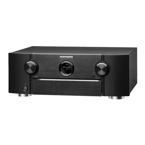
AV Surround Receiver
SR6011
• For purposes of improvement, specifications and design are subject to change without notice.
• Please use this service manual with referring to the operating instructions without fail.
• Some illustrations using in this service manual are slightly different from the actual set.
Service Manual
Click here!
On-line service parts list
http://dmedia.dmglobal.com/Document/DocumentDetails/23034
Online Parts List
(P5 to P7)
WEB owner's manual
http://manuals.marantz.com/SR6011/NA/EN/index.php
http://manuals.marantz.com/SR6011/EU/EN/index.php
http://manuals.marantz.com/SR6011/AP/ZH/index.php
CAUTION IN SERVICING
ELECTRICAL
MECHANICAL
REPAIR INFORMATION
UPDATING
Please refer to the MODIFICATION NOTICE.
Ver. 4
Advertisement
Table of Contents

Related Manuals for Marantz SR6011


Summary of Contents for Marantz SR6011
- Page 1 Service Manual Ver. 4 AV Surround Receiver Click here! SR6011 On-line service parts list http://dmedia.dmglobal.com/Document/DocumentDetails/23034 Online Parts List (P5 to P7) WEB owner’s manual http://manuals.marantz.com/SR6011/NA/EN/index.php http://manuals.marantz.com/SR6011/EU/EN/index.php http://manuals.marantz.com/SR6011/AP/ZH/index.php CAUTION IN SERVICING ELECTRICAL MECHANICAL REPAIR INFORMATION UPDATING • For purposes of improvement, specifications and design are subject to change without notice. Please refer to the MODIFICATION NOTICE.
-
Page 2: Caution In Servicing
CAUTION IN SERVICING SAFETY PRECAUTIONS NOTE FOR SCHEMATIC DIAGRAM NOTE FOR PARTS LIST INSTRUCTIONS FOR HANDLING SEMICONDUCTORS AND OPTICAL UNIT Online Parts List Accessing the Parts List Logging in to New SDI and Accessing the Parts List Accessing the Part List from the Model Asset Screen PRINTED CIRCUIT BOARDS Parts Table Downloading the Parts List as an Excel File Revision History... -
Page 3: Safety Precautions
SAFETY PRECAUTIONS ◎ Make a safety check after servicing! The following items should be checked for continued protection of the customer and the service Check that all screws, parts and wires removed or disconnected when servicing have been put back technician. -
Page 4: Note For Schematic Diagram
NOTE FOR SCHEMATIC DIAGRAM WARNING: Parts indicated by the z mark have critical characteristics. Use ONLY replacement parts recommended by the manufacturer. CAUTION: Before returning the set to the customer, be sure to carry out either (1) a leakage current check or (2) a line to chassis resistance check. - Page 5 Online Parts List Accessing the Parts List Logging in to New SDI and Accessing the Parts List (1) Click the URL link on the cover of the service manual. (1) Access New SDI from the URL below. Examples of display <http://dmedia.dmglobal.com>...
-
Page 6: Revision History
Accessing the Part List from the Model Asset Screen Downloading the Parts List as an Excel File (1) Display Model Asset from New SDI. (1) Displays the Parts List. Click the Download icon. (2) Click the section displayed as ▼ Link to Part Lists under the model name. NOTE : If the ▼... - Page 7 Searching Part Numbers or Ref. Numbers You can search a Parts List for part numbers or Ref. numbers. (1) Enter the part number or Ref. number in the search window of the Parts List, and press the search button. (2) The search results are displayed. The name of the sheet in which the search part is used and the part’s line are displayed.
-
Page 8: Initializing This Unit
CAUTION IN SERVICING. Initializing This Unit Make sure to initialize this unit after replacing the microcomputer or any peripheral equipment, or the digital PCB. 1. Press the power button to turn off the power. 2. While holding down buttons "TUNER PRESET CH -" and "TUNER PRESET CH +" simultaneously, press the power button to turn on the power. -
Page 9: Schematic Diagrams
ELECTRICAL SCHEMATIC DIAGRAMS BLOCK DIAGRAM SCH35_FRONT SCH36_HDAM1 SCH01_DIGITAL CONNECT ANALOG AUDIO DIAGRAM SCH37_HDAM2 SCH02_DIGITAL POWER DIGITAL AUDIO DIAGRAM SCH38_SMPS SCH03_MAIN CPU VIDEO DIAGRAM SCH04_EXPANDER HDMI DIAGRAM PRINTED CIRCUIT BOARDS SCH05_CPU LEVEL CHG POWER DIAGRAM SCH06_DIR DIGITAL SCH07_AUDIO PLD INPUT, F-HDMI, CONNECT-2, CONNECT-3, SCH08_DSP1 CONNECT-4 WIRING DIAGRAM... - Page 10 SCHEMATIC DIAGRAMS SCH01_DIGITAL CONNECT TO 0A (PAGE 2_B1) TO DIGITAL SUPPLY DAC input BN27A L1001 CH1: DATAF R1021 OPEN CPUPOWER R1022 OPEN M3.3V R1023 OPEN DGND CH2: DACLRCK BN24A TO CN24A BN26A RC_IN KILLIR_MZ A-7V TO CN26A TO 2A RC_OUT_MZ A+7V FRONT_IRIN CH3: DACBCK...
- Page 11 SCH02_DIGITAL POWER PJ02 PJ01 CN903 L1221 BLM21PG221SN1 L1222 DGND D5.2V BLM21PG221SN1 L1223 D5.2V BLM21PG221SN1 TO BN901 M_RESET CEC1.1V-2 DGND 1.62A R1111 DV_POWER2 DGND DV1.8V IC111 CEC_POWER L1113 L1111 TPS563200DDCR R1201 IC120 L1203 L1224 MAINPOWER 1.34A CB03YTYH600 L1201 CB03YTYH600 TPS563200DDCR OPEN BLM21AG121SN1 L1112 L1115...
- Page 12 SCH03_MAIN CPU TO 6D TO 5D TO A4 TO B9 TO B3 TO B8 TO C0 TO C1 TO LEVEL CHG. (PAGE 5) TO DIGITAL CNT (PAGE 1) A3,4 TO C2 R1577 4.7K DA_MS DA_MC R1578 OPEN DA_MDI R1579 OPEN R1581 OPEN DSP_ICS...
- Page 13 SCH04_EXPANDER TO 8E TO 9E TO 1F TO 2F TO A7 TO B5 TO B1 TO B6 TO A9 TO B7 TO B0 TO B2 (PAGE 16_C6) DIGITAL CNT (PAGE 13_A4) (PAGE 17_D6) (PAGE 14_A3) VIDEO PLD PAGE 1 HDMI SW2 HDMI TX HDMI SW1 R1702...
- Page 14 SCH05_CPU LEVEL CHG TO D6 (PAGE 3_D5) TO B4 TO D4 FROM MAIN CPU TO DIGITAL CONNECT (PAGE 1_A4) TO DIGITAL SUPPLY POWER (PAGE 2_B1) R1953 4.7K Q1918 RT1N141C C1915 IC191 SN74LVC244APWR R1954 T206 T186 R1955 T185 3.3K R1967 R1956 R1957 2SC3052 2SC3052...
- Page 15 SCH06_DIR DIR output DIR input CH1: DIRDATA CH1:RXIN0 ZONE1 DIRMCK CH2: LRCK DIRBCK DIRLRCK DIRDATA R2045 Z3DIRSPDIF CH3: DIRBCK R2044 Z2DIRSPDIF R2046 3.3K DATAAD R2047 TO 4F DIRDOUT R2056 OPEN R2035 OPEN HDMI SW1 DIRDIN R2063 DIRADLRCK DIRRST DIRRST (PAGE 14_C1) R2064 DIRADBCK MPIO_B1...
- Page 16 SCH07_AUDIO PLD MCU_VL_MUTE MCU_VL_MUTE TO E6 VOLUME_MUTE VOLUME_MUTE PLDAERR1 PLDAERR1 Z2PLDAERR Z2PLDAERR Z3PLDAERR Z3PLDAERR IC222 OPEN JTAG_TMS JTAG_TDOO JTAG_TDOO JTAG_TDI JTAG_TDI JTAG_TDI JTAG_TCK JTAG_TMS JTAG_TMS TO F3 R2249 TDO1_TDI2 JTAG_TCK JTAG_TCK APLD_CS APLD_CS APLD_DI APLD_DI APLD_CK APLD_CK R2279 RXMCK/DSDMCK BCOBCK_SCK IO-001 IO-081 R2278...
- Page 17 SCH08_DSP1 TO G2 TO 1H TO 2H TO 3H TO 4H TO E7 TO 0H TO G3 FROM AUDIO PLD FROM A.PLD PART TO DSP2 PART FROM MAIN CPU PART TO DSP2 PART TO DSP4 PART TO DSP3 PART TO DSP2 PART (PAGE 7_A5) (PAGE 8-2_D5) (PAGE 8-2_D3)
- Page 18 SCH09_DSP2 TO H0 TO H1 TO G4 TO H4 TO A.PLD PART FROM DSP1 PART FROM DSP1 PART FROM DSP1 PART (PAGE 8-1_D3) (PAGE 7_A4) (PAGE 8-1_D2) (PAGE 8-1_D4) C2645 IC262 A3V56S40GTP-60 1000P 256M BIT SDRAM C2637 R2635 C2646 VDD_INT DAI_P09 DSP2_FLAG0 R2643...
- Page 19 SCH10_DSP3 TO G1 TO 5H TO G5 TO H3 ADUDIO PLD PART FROM DSP1 PART TO DSP4 PART FROM AUDIO PLD (PAGE 8-4_D5) (PAGE 7_A4) (PAGE 8-1_D2) (PAGE 7_A5) IC272 C2745 A3V56S40GTP-60 256M BIT SDRAM 1000P C2737 C2746 0.1 VDD_INT DAI_P09 DSP3_FLAG0 R2745...
- Page 20 SCH11_DSP4 TO H5 TO G6 TO H2 FROM DSP3 PART ADUDIO PLD PART FROM DSP1 PART (PAGE 8-3_D4) (PAGE 7_A4) (PAGE 8-1_D2) IC282 C2855 1000P A3V56S40GTP-60 256M BIT SDRAM C2847 C2856 0.1 VDD_INT DAI_P09 R2845 DSP4_FLAG0 FLAG0 DAI_P05 R2846 4.7K DQ15 DSP4D0 C2857 0.1...
- Page 21 SCH12_ADC TO G7 TO D9 TO F6 TO AUDIO PLD TO MAIN CPU TO DIR (PAGE 7_A3) (PAGE 3_C6) (PAGE 6_C4) A+5V AD_VDCOM ADINL ADINR DAGND TO A2 C3055 C3056 C3057 1000P C3058 1000P C3061 1000P C3062 1000P C3063 1000P C3064 1000P C3066 1000P C3067 1000P...
- Page 22 SCH13_ZONE DAC TO AUDIO PLD (PAGE 7_A2) TO G8 IC323 BU33TD3WG VIN VOUT ZONE_DAC STBY ZONE2 DAC IC321 PCM5100PWR DVDD CPVDD C3201 C3203 DGND CAPP C3202 2.2/6.3V LDOO CPGND XSMT CAPM Z2DACMUTE VNEG LRCK OUTL R3203 Z2DACLRCK DAZONE2L OUTR R3204 TO DIGITAL CONNECT Z2DACDATA DAZONE2R...
- Page 23 SCH14_CY920 BASIC CONNECTOR EXTENDED CONNECTOR CN501 CJP64GA321ZP CN502 CJP64GA321ZP CN511 CJP07GA193ZY 10022H-07C R5081 open DGND T162 DEBUG_RX T201 DEBUG_TX T207 3.3V T161 NET3.3V T266 R5057 open R5058 open R5059 open R5060 open R5063 CN512 CN512 CJP07GA193ZY NET1.2V 10022H-07C TO CN401 IC501 MP:open MX25L25635FMI-10G...
- Page 24 SCH15_VIDEO DECODER TO C5 FROM DIGITAL SUPPLY POWER (PAGE 2_B3) L3501 L3506 L3509 BLM21PG221SN1 BLM21PG221SN1 BLM21PG221SN1 L3502 L3510 L3507 BLM21PG221SN1 BLM21PG221SN1 BLM21PG221SN1 L3503 L3511 BLM21PG221SN1 BLM21PG221SN1 BLM21PG221SN1 L3508 BLM21PG221SN1 L3512 BLM21PG221SN1 L3504 L3513 L3505 BLM21PG221SN1 BLM21PG221SN1 C3502 OPEN C3503 OPEN C3504 REFP REFN...
- Page 25 SCH16_HDMI SW2 CEC5V CEC3.3V L3801 BLM21PG221SN1 VDD33 Q3841 CEC1.1V-2 HDMI_SW2 DGND Q3842 RT1N141C HPD1 L3802 +5V_1 HPD_1 AVDD33TX BLM21PG221SN1 R3845 RX1_C- TO C9 RT1N141C RX1_5V RX1_C+ RX1_0- 19.HP DET 18.+5V RX1_0+ 17.GND RX1_1- L3809 R3847 16.DDC DATA RX1_1+ RX1_DDCDA AVDD33RX CLZBLM21PG300SN1D 15.DDC CLK R3848...
- Page 26 SCH17_HDMI SW1 Z2_CEC5V CEC5V HDMI_SW2 P2_C- CEC3.3V L3901 P2_C+ VDD33 BLM21PG221SN1 P2_D0- CEC1.1V-1 P2_D0+ DGND P2_D1- P2_C- P2_D1+ P2_C- P2_C+ P2_D2- L3902 P2_C+ AVDD33TX BLM21PG221SN1 TO C8 P2_D0- P2_D0- P2_D2+ P2_D0+ P2_D0+ P2_D1- P2_D1- RX5_C- P2_D1+ RX5_C+ P2_D1+ P2_D2- RX5_0- P2_D2- L3910 AVDD33RX...
- Page 27 SCH18_VSP & IP & OSD TO C6 FROM DIGITAL POWER SUPPLY (PAGE 2_B3) L4001 CB03YTYH600 L4002 CB03YTYH600 L4003 L4008 L4013 CB03YTYH600 CB03YTYH600 CB03YTYH600 L4004 L4010 CB03YTYH600 CB03YTYH600 L4016 CB03YTYH600 L4005 L4012 L4014 CB03YTYH600 CB03YTYH600 CB03YTYH600 IC403 IC402 A3R12E40DBF-8E L4006 A3R12E40DBF-8E 512Mbit DDR2 SDRAM L4015 512Mbit DDR2 SDRAM...
- Page 28 SCH19_VIDEO PLD TO C7 TO G9 FROM DIGITAL POWER TO AUDIO PLD (PAGE 2_B3) (PAGE 7_D1) MCU&CY920 VPLD_TRANS2 VPLD_TRANS2 VPLD_TRANS1 FROM EXPANDER VPLD_TRANS1 ADV8003 VPLD_TRANS0 VPLD_TRANS0 (PAGE 4_C4) RGB/YC R4201 R4216 RGB/YC PO8KI_C0/B0 IO-001 IO-081 PO8KI_Y9/R5 NET/HDMI NET/HDMI R4217 IO-002 IO-082 PO8KI_Y6/R2 SD/HD...
- Page 29 SCH20_HDMI TX & SCALER CEC5V CEC3.3V L4308 AVDD11TX CEC1.1V-3 L4301 VDD33 BLM21PG221SN1 C4403 OPEN DGND L4305 BLM21PG221SN1 C4402 OPEN VDD11 C4401 OPEN BLM21PG221SN1 JK432 C4400 OPEN HDMI_OUT OPEN L4321 PTX0_2+ 1.D2+ L4310 AVDD11RX L4309 C4409 OPEN TO D1 AVDD33RX PTX0_2- 2.D2 SHIELD CLZBLM21PG300SN1D C4408...
- Page 30 A-7V C4675 C4679 C4681 10/50V R4831 PREZ2L AGND 10/50V 0.01uF C4805 R4811 C4811 R4815 C4819 R4821 C4823 R4825 C4825 SR6011 SR7011 220/10V 0.022u 6800P 10/50V 4.7K 100P 10/50V C4837 3300P PREZ2L 0.01uF PREZ2L C4839 PREZ2R C4629 0.1uF OPEN R4817 R4819...
- Page 31 R8832 0.01uF C8825 0.1/50V C8829 C8835 R8829 R8833 R8839 R8821 R8902 P_PREH2MUTE 22/50V 22/50V P_PREZ2R P_PREASS3R P_PREZ3L R8951 *MODEL OPTION SR6011 SR7011 OPEN OPEN R8952 P_PREZ3R JK875 CJJ4M056W C8803 R8803 R8805 C8807 R8811 R8820 22/50V 22/50V R8819 470K R8815 R8817 C8820 0.01uF...
- Page 32 SCH23_HDAM CNT & FHDMI Q1001 Q1002 RT1P141C R1003 RT1N241C C1001 R1004 19.HP DET 0.1uF 18.+5V 17.GND 16.DDC DATA 15.DDC CLK 14.NC 13.CEC 12.CK- L1001 CEC5V 60R/3A 11.D1 SHIELD CN101 10.CK+ 9.D0- 8.D1 SHIELD 7.D0+ 6.D1- CEC3.3V 5.D2 SHIELD L1002 DDCD_SDA 4.D1+ DDCD_SCL 60R/3A...
- Page 33 VGND DEC_PB_IN VGND TO CN21B DEC_PR_IN VGND VGND VGND VIN_A VIN_B VIN_C COMP_SW2 # CVBS INPUT SW (NJM2595) COMP_SW1 STATUS OUTPUT SR6011 SW2 SW3 SW4 SW5 VOUT1 VOUT2 MUTE MUTE MUTE VIN3 VIN3 CBL/SAT VIN4 VIN4 VIN5 VIN5 BLU-RAY VIN2...
- Page 34 SCH25_RC-5 RC-5 R5311 BN27B R5312 Q5313 RT1P141C BN27B 60R/3A(BEAD) L5311 60R/3A(BEAD) M3.3V L5312 Q5311 Q5312 DGND L5313 RT1P141C 60R/3A(BEAD) RT1N141C RC_IN L5314 60R/3A(BEAD) KILLIR_MZ RC_OUT_MZ FRONT_IRIN L5315 60R/3A(BEAD) FLASHER_IN_MZ REMOTE3.3V Q5314 232O_MI RT1P141C 232I_MO TRIGGER_1 JK531 B/P_IRIN_AVR R5314 D5311 OPEN Q5315 R5313 2SC3052...
- Page 35 SCH26_RS232C_TRIGGER IR / FLASHER RS232C/TRIGGER IC521 C5237 C5236 ILX3232DT 50V/0.1uF 16V/10uF C5231 C5235 OPEN C5245 50V/0.01uF 50V/0.1uF 50V/0.1uF C5246 OPEN JK521 C5247 50V/0.1uF JK525 D5231 Q5251 OPEN RT1P141C T1_O R5234 PJ-308-02 R1_I R5233 RS-232C D5232 C5233 Q5252 R1_O OPEN 2SC3052 50V/0.1uF C5234 T1_I...
- Page 36 TU_+5V TU_+5V TU_GND TU_GND TU_CE TU_CE TU_RST TU_RST TU_INT TU_INT TU_RXMO/SCL TU_RXMO/SCL TU_TXMI/SDA TU_TXMI/SDA FROM/TO RC-5/MX-PORT PART TU_GND CN27C SR6011 PAGE 20_A5 CN961 TO BN27B CN27C 12511HS-13 CN28C J9631 TO BN961 SR6011 TO BN28B CN28C J9633 CN28C C125Z1-07 CN27C C125Z1-15...
- Page 37 SCH28_FRT CNT CN21A CN25A CN26A CN24A TO BN21A TO BN25A TO BN26A TO BN24A FROM/TO DIGITAL CON. PART FROM/TO DIGITAL CON. PART PAGE 1_B3 FROM/TO DIGITAL CON. PART FROM/TO DIGITAL CON. PART FRT CNT CONNECT B PAGE 1_D3 PAGE 1_D5 PAGE 1_B5 CN25A CN26A...
- Page 38 SCH29_MAIN DAC1 A+5V C3055 0.1uF TO K0 A-7V C3056 0.1uF C3057 1000pF A+7V C3058 1000pF DAGND C3059 OPEN C3060 OPEN C3061 1000pF C3062 1000pF C3063 R3017 1000pF 150K C3064 0.1uF R3021 C3065 0.1uF C3066 0.1uF C3017 R3013 R3025 R3027 C3067 1000pF C3068 270pF...
- Page 39 SCH30_MAIN DAC2 A+5V C3147 0.1uF TO K1 A-7V C3148 0.1uF C3149 1000pF A+7V C3150 1000pF DAGND C3151 OPEN C3152 OPEN C3153 0.1uF C3154 R3125 150K 0.1uF C3155 1000pF R3123 C3156 1000pF ASSIGNL1 C3125 R3113 R3121 R3127 270pF R3111 R3119 (GRM21) C3130 (GRM21) 16V/220uF...
- Page 40 Q9231 A_GND A-7V OPTION B DA_+5V C9701 C9702 RT1N237C RT1N237C RT1N237C RT1N237C RT1N237C RT1N237C RT1N237C RT1N237C RT1N237C RT1N237C MODEL SR7011 SR6011 0.1u/250V 0.1u/250V AREA CN25D C9703 CN25D C9705 C125Z1-25 71V/15000uF 71V/12000uF C9706 0.1u/250V H/PL H/PGND H/PR H/P_RLY H/P_RLY D9701 FRONT_RLY...
- Page 41 MAX 130mA 2SA2166 R9410 0(3216) R9411 OPEN Q9416 KTC3964 Q9414 RT1P144C Q9413 RT1N237C Q9415 RT1N237C REGULATOR PART OPTION E CN77D MODEL SR7011 SR6011 AREA TU+5V C9311 F9336 16V/3300uF 16V/1000uF A+7V C9312 OPEN A+7V D9313 R9331 R9325 AGND OPEN OPEN OPEN AGND...
- Page 42 SCH33_5CH AMP Point C1 D7102 R7116 R7117 63.7V OPEN R7118 R7138 R7115 1.2K(1608) 1.2K(1608) 1W/270 R7119 PTC 115'C 470 ohm D7101 OPEN CN715 1W/270 62.9V OPEN R7137 Q7114 D7118 Q7138 58.5V MMBT5401 MMBT5401 1SS133M 1.1V 680K(1608) 0.6V C7111 C7108 Q7118 R7129 D7139 R7143...
- Page 43 SCH34_4CH AMP R7616 R7617 D7602 OPEN R7615 R7618 R7638 1.2K(1608) 1.2K(1608) R7619 D7601 OPEN 1W/270 CN765 PTC 115'C 470 ohm 1W/270 OPEN Q7614 R7637 Q7638 D7618 MMBT5401 680K(1608) MMBT5401 C7611 1SS133M C7608 Q7800 Q7618 R7629 R7643 D7639 R7639 OPEN MMBT5401 OPEN KTA1024Y 1W/22...
- Page 44 SCH35_FRONT SR6011 FRONT B'D BK604 JW604 GP1261AI LUG61 FL601 CUP12383-2 VOLUME CMD1A569-V1 Front Panel R6028 R6012 Q6001 Q6022 OPEN OPEN 163mA R6112 R6114 FLRST CPU POWER CPUPOWER CN69A C6010 4.7K CN69A 15mA Q6024 SWM3.3V SWM3.3V FPC 1.0-11S-40PW RT1N141C 470uF/6.3V OPEN...
- Page 45 SCH36_HDAM1 HDAM1 PART AMP_FL P_PREFL AMP_FR P_PREFR BN87D4 BN87D4 CJP21HJ282Z AMPSELFHR AGND AMPSELFHL AGND AMPSELFWR AGND R8105 Q8121 R8127 Q8155 R8155 Q8171 R8177 Q8127 Q8105 Q8113 KTA1504S Q8135 Q8163 KTA1504S Q8177 Q8185 AMPSELFWL KTA1504S KTC3875S KTA1504S KTC3875S KTA1504S KTC3875S KTC3875S KTA1504S AGND R8117...
- Page 46 SCH37_HDAM2 HDAM2 PART AMP_FWL AMP_FWR AMP_FHL AMP_FHR Q8321 Q8371 R8305 R8327 Q8355 R8355 Q8377 R8377 Q8305 Q8313 Q8327 Q8335 Q8363 Q8385 KTA1504S KTA1504S KTA1504S KTA1504S KTA1504S KTC3875S KTA1504S KTC3875S KTC3875S KTC3875S C8335 C8385 R8317 R8367 R8335 PREFHL R8385 PREFWL 47/25V 47/25V C8301 C8351...
- Page 47 J9004 AV7703 AC220 ~ 240V : T 1A L 250V C3A206 R9027 4.7K(0.2W) C9027 OPEN J9016 C3A206 J9015 OPTION OPTION C3A206 Ref. NO SR6011/SR7011N/K/F SR7011/U AV7703/N AV7703/U AC INPUT ZD921 ZD908 R9008 R9009 R9010 R9014 R9015 R9016 C9006 C9007 C9008...
- Page 48 PRINTED CIRCUIT BOARDS DIGITAL Lead-free Solder When soldering, use the Lead-free Solder (Sn-Ag-Cu). DIGITAL (A SIDE) D3804 DA_7 CK_7 DA_6 CK_6 DA_5 CK_5 DA_3 CK_3 DA_2 CK_2 D4317 JK432 DA_1 DA_M1 D4316 T192 TP39 D3964 R3976 R4353 R3848 HPD_Z2 HPD_M2 JK394 JK393 +5V_6...
- Page 49 INPUT, F-HDMI, CONNECT-2, CONNECT-3, CONNECT-4 INPUT (A SIDE) INPUT (B SIDE) F_HDMI (A SIDE) F_HDMI (B SIDE) JK101 IC101 R1005 C1020 C1003 C1019 C1018 C1005 T280 C1006 R1013 T292 C1023 MI ICT FCT1 FCT2 RP C1015 T293 C1022 R1001 Q1001 Q1002 T282 T283...
- Page 50 VIDEO (A SIDE) VIDEO (B SIDE) SIDE CNT (A SIDE) CN27A JW961 CN23A R5212 J9615 J9606 R5213 C5211 J9621 J9616 J9622 Q5211 R5211 J9623 SR6011 J9617 CN28C TRG+12V C5213 J9624 R5210 J9633 SR6011 J9625 C5212 CN27C CN28C CN27C J9631 J9627 R5231...
- Page 51 SPK, SPK H2L, GUIDE TRANS, GUIDE TOP, GUIDE SIDE SPK (A SIDE) SPK H2L (A SIDE) SPK H2L (A SIDE) CN951 JK930 CUP12852Z_A-2 MP J9252 J9253 C9539 JK924 C9534 JK929 JK923 JW930A JK928 JK931 C9541 JK926 C9536 J9254 C9537 JK925 C9535 C9533 JK921...
- Page 52 5CH AMP, 4CH AMP 5CH AMP (A SIDE) 5CH AMP (B SIDE) 4CH AMP (A SIDE) 4CH AMP (B SIDE) J7128 D7402 D7401 C7423 R7415 R7417 R7416 R7435 Q7439 C7419 D7419 R7735 D7702 R7715 R7135 C7723 R7136 D7102 R7115 R7717 R7716 C7123 C7719...
- Page 53 FRONT, HDMI FFC TOP FRONT (A SIDE) FRONT (B SIDE) HDMI FFC TOP (A SIDE) JW602 R6114 R6115 CUP12866-3 HDMI FFC TOP R6122 Q6013 C6076 R6036 R6037 D6001 C6004 C6061 C6018 D6002 C6019 C6020 C6024 R6106 C6021 C6060 C6002 R6108 C6022 C6023 R6104...
- Page 54 FRONT CNT, TUNER, BKT, HDAM, SMPS FRONT CNT (A SIDE) FRONT CNT (B SIDE) SMPS (A SIDE) SMPS (B SIDE) Sec. Sec. Sec. Sec. Pri. Pri. Pri. Pri. Pri. Pri. Sec. Sec. Pri. Pri. 2 1 . P _ R L G N D Sec.
-
Page 55: Level Diagram
LEVEL DIAGRAM FRONT ch SR6011 LEVEL DIAGRAM FRONT ch NJU72343 NJU72750 ANALOG HDAM H/POUT NJU72751 NJU72750 SPEAKER LINE IN + GAIN ADJ. - PCM1690 MIC IN + + + AK5358 - - MUTE PRE OUT TO ZONE2 x4pcs EXT IN +30dB 4.24Vrms/8Ω... - Page 56 CENTER / SURROUND ch SR6011 LEVEL DIAGRAM CENTER/SURROUND ch NJU72343 HDAM SPEAKER + GAIN ADJ. PCM1690 + + - - MUTE PRE OUT x4pcs EXT IN +30dB 4.24Vrms/8Ω Volume IC: NJU72343 NON CLIP MAX SIGNAL LEVEL 4.2Vrms SPK OUT Differential Out PCM1690 2.83Vrms=0dBFS...
- Page 57 SUBWOOFER ch SR6011 LEVEL DIAGRAM SUB WOOFER ch NJU72343 HDAM GAIN ADJ. PCM1690 + + - - MUTE PRE OUT x4pcs EXT IN +30dB +30dB FULL SCALE LEVEL Volume IC: NJU72343 NON CLIP MAX SIGNAL LEVEL 4.2Vrms Differential Out PCM1690 DOLBY LIMIT LEVEL (ALL ch -3dBFS) 2.83Vrms=0dBFS...
- Page 58 ASSIGN1 / 2 (SURR.BACK / HEIGHT1 / HEIGHT2) ch SR6011 LEVEL DIAGRAM ASSIGN1/2 (SURROUND BACK/HEIGHT1/HEIGHT2) ch NJU72343 HDAM NJU72750 SPEAKER + GAIN ADJ. PCM1690 + + - - MUTE PRE OUT x4pcs EXT IN +30dB 4.24Vrms/8Ω Volume IC: NJU72343 NON CLIP MAX SIGNAL LEVEL 4.2Vrms...
- Page 59 ZONE2 ch SR6011 LEVEL DIAGRAM ZONE2 NJU72750 LINE To MAIN MUTE PRE OUT MONO PCM5100 NJW1194V MONO Z2 DAC NJU72750 + SPEAKER +30dB NJW1194V MAX. OUTPUT 4.2Vrms SP OUT 4.24Vrms/8Ω PCM5100 MAX. SIGNAL LEVEL 2.0Vrms=0dBFS +20dB +20dB +29dB +10dB -10dBFS +10dB -20dBFS(DIG.IN)
- Page 60 BLOCK DIAGRAM ANALOG AUDIO DIAGRAM SR6011/SR7011 ANALOG AUDIO BLOCK RY871 PRE FL 11.2ch Processing NJU72751V PRE FR Main L PRE CEN DAFL ADC L EXT_FL EXT_FL PRE SW1 EXT_FR EXCEPT AVRX4300H EXT_C SW A x 4 HDAM EXT_C PRE SL...
- Page 61 DIGITAL AUDIO DIAGRAM SR6011 DIGITAL AUDIO BLOCK(ADI) DIRRST #146 DIRCE #143 DIRDIN #141 DIRDOUT #144 DIRCLK #145 Z2DIRSPDIF 24.576MHz DIGTAL IN COAX.0 DATAAD ADINL MAIN COAX.1 OPT.0 ZONE2 DIRSLRCK OPT1(TV) OPT.0 DIRSBCK ADINR OPT.1 OPT.1 (To MAIN DIR) BCOSPDIF DIRSMCK...
- Page 62 VIDEO DIAGRAM SR6011 ANALOG VIDEO BLOCK CBL/SAT CBL/SAT_V DVD_V Blu-Ray Blu-Ray_V V.AUX(FRONT) V.AUX_V CVBS OUT CVBS MONITOR COMPONENT OUT COMPONENT OUT Y CBL/SAT_Y COMPONENT OUT PB CBL/SAT CBL/SAT_PB COMPONENT OUT PR CBL/SAT_PR NJM2595MTE1 V_AUX_V DVD_Y CBL/SAT_V DVD_V DVD_PB Blu-Ray_V DVD_PR...
- Page 63 HDMI DIAGRAM SR6011 HDMI BLOCK HDMI SW2(MN864788) P3 RX HDMI IN1 (CBL/SAT) MAIN P0 TX P2 RX HDMI IN2 HDMI TX(MN864787) (DVD) P1 RX P1 RX P1 TX HDMI IN3 (BLU-RAY) P0 RX P0 RX HDMI Rx 600MHz 4K/2K 600MHz...
-
Page 64: Power Diagram
POWER DIAGRAM SR6011 POWER BLOCK DIAGRAM Current value Max Current (Safety Standard Condition) HI+B LOW+B RY931 428mA S1(AMP+B,-B) +12V(RELAY) SPK Relay(5EA)+ Small Relay(1EA)+H/L Relay(1EA)+Fan(2EA) (294mA) 222.5 + 12.5 + 33 + 160 = 428mA LOW-B HI-B 33mA +3.3V (Z2 DAC) BU33TD3WG (24.7mA) -
Page 65: Wiring Diagram
WIRING DIAGRAM WIRING DIAGRAM (SR6011) WiFi Antenna WiFi Antenna HEIGHT PCB PCB CUP12852Z-2 CN321 WAFER/5P/2mm CJP05GI288ZY BN961 CN951 WAFER/3P/2.5mm CJP03GI289ZY DIGITAL PCB CUP12871Z BN951 CUP12846Z WIRE/3P/2.5mm/50mm Network PCB INLET CWB1E0030503D CN781 CN704 WAFER/6P/2mm WAFER/7P/2mm (PROT.LINE) (PROT.LINE) CN431 CJP06GA208ZY CJP07GA208ZY CON1... - Page 66 XTAL Pins for a crystal resonator (Xin=12MHz × 10) Ground pin EXTAL/P36 EXTAL Pins for a crystal resonator (Xin=12MHz × 10) Power supply pin NC(X4300/ SR6011)/ Front trap door open/close detect input pin (High:Door UPSEL/P35(IN)/NMI DOOR M3VPu/ open) DET(SR7011/ AV7703)
- Page 67 IRQ14 User Boot Mode) AV7703(NA))/ P26/TXD1 HDRADIO/TUNER control VIDEO I2C control pin for ADV8003/ ADV7850/ PC6/RXD8/IRQ13 AVSDA TU SCLK(X4300H/ 3VPu ADVM2000(except SR6011) SR6011(ALL),SR7011/ VIDEO I2C control pin for ADV8003/ ADV7850/ AV7703(EU/CH/JP)) PC5/SCK8 AVSCL 3VPu ADVM2000(except SR6011) P25/RXD3 VOL DATA Volume control pin (NJU72343)
- Page 68 FL RST FL display control pin THERMAL A(X4300/ P67/IRQ15 FL CE FL display control pin P93/AN117 SR6011/ Protection detect signal input pin (for power TR) SW3VPu TRDATA1/PG3 FL CLK FL display control pin SR7011)/ FL DATA FL display control pin...
- Page 69 PCM9211 www.ti.com SBAS495 – JUNE 2010 AD8195 PIN CONFIGURATIONS AD8195ACPZ (F-HDMI : IC101) PCM9211 (DIGITAL : IC202) PT PACKAGE LQFP-48 PIN CONFIGURATION AND FUNCTION DESCRIPTIONS (TOP VIEW) ERROR/INT0 VDDRX 30 AVCC PIN 1 30 AVCC NPCM/INT1 RXIN1 29 PE_EN INDICATOR PIN 1 29 PE_EN INDICATOR...
- Page 70 PCM9211 PCM9211 BLOCK DIAGRAM www.ti.com SBAS495 – JUNE 2010 BLOCK DIAGRAM DESCRIPTION NAME FILT TOLERANT AUXIN 0 26 MS/ADR1 Software control I/F, SPI chip select / I2C slave address AUTO RXIN7 setting1(2) RXIN 0 RXIN0 SCKO DOUT RXIN 1 RXIN1 MAIN OUTPUT 27 MODE...
- Page 71 A3V56S40GTP 256M Single Data Rate Synchronous DRAM ADSP21487KSWZ4B (DIGITAL : IC251 / IC261 / IC271 / IC281) A3V56S40GTP-60 (DIGITAL : IC252 / IC262 / IC272 / IC282) Pin Configuration (Top View) PIN 1 PIN CONFIGURATION (TOP VIEW) GND PAD DQ15 (PIN 177) DQ14 DQ13...
- Page 72 PCM1690 (FRONT CNT : IC301, IC311) TERMINAL PULL- DESCRIPTION NAME DOWN TOLERANT VCC1 25 — — — Analog power supply 1, +5 V VCOM 26 — — — Voltage common decoupling AGND1 27 — — — Analog ground 1 RSV2 28 —...
- Page 73 SLAS764 – MAY 2011 www.ti.com SBAS448A – OCTOBER 2008 – REVISED JANUARY 2009.............................. www.ti.com DEVICE INFORMATION FUNCTIONAL BLOCK DIAGRAM TERMINAL FUNCTIONS, PCM510x PCM5100 (DIGITAL IC321) PCM1690 FUNCTIONAL BLOCK DIAGRAM PCM510X (top view) VOUT1+ DIN1 DIN2 VOUT1- DIN3 Audio Interface DIN4 VOUT2+ LRCK VOUT2-...
- Page 74 NJU72343 (INPUT : IC471/IC491) NJU72751 (INPUT : IC475) No. Symbol Function No. Symbol Function No. Symbol Function No. Symbol Function AREF Analog reference potential DATA IC control data input Power supply(+) CLOCK IC control clock input Address selection CLOCK IC control clock input ADR0 Address selection pin 0 InA2...
- Page 75 G Bipolar Technology G Package Outline DIP16,DMP16 GENERAL DESCRIPTION PACKAGE OUTLINE The NJM2586A is a wide band 3-input 1-output 3-circuit video I PIN CONFIGURATION and BLOCK DIAGRAM NJM2595MTE1 ( amplifier. It is suitable for Y, Pb, and Pr signal because frequency IC511) VIDEO : range is 50MHz.The NJM2586A is suitable for AV receiver, STB,...
- Page 76 PATTERN DETAIL 2. FL DISPLAY FLD (GP1261AI) (FRONT : FL601) 42-1 43-1 44-1 45-1 46-1 47-1 48-1 42-2 43-2 44-2 45-2 46-2 47-2 48-2 42-3 43-3 44-3 45-3 46-3 47-3 48-3 42-4 43-4 44-4 45-4 46-4 47-4 48-4 PIN CONNECTION 42-5 43-5 44-5...
- Page 77 MECHANICAL DISASSEMBLY Flowchart 1. FRONT ASSY 2. RADIATOR ASSY 3. REAR PANEL 4. DIGITAL PCB 5. VIDEO PCB 6. INPUT PCB 7. TUNER PCB 8. SPK PCB 9. SMPS PCB 10. TRANS EXPLODED VIEW PACKING VIEW...
- Page 78 DISASSEMBLY Flowchart • Remove each part following the flow below. • Reassemble the removed parts in the reverse order. • Read "SAFETY PRECAUTIONS" before reassembling the removed parts. • If wire bundles are removed or moved during adjustment or part replacement, reshape the wires after completing the work. Failure to shape the wires correctly may cause problems such as noise. •...
-
Page 79: Front Assy
• The photographs with no shooting direction indicated were taken from the top of the unit. (1) Remove the screws. • Photos of SR6011 U are used in this manual. The viewpoint of each photograph (Shooting direction : X) [View from the top] ↑Front side↑... -
Page 80: Radiator Assy
(3) Remove the connector. 2. RADIATOR ASSY Proceeding : TOP COVER → FRONT ASSY → RADIATOR ASSY (1) Remove the screws. View from the bottom (2) Remove the screws. Cut the wire clamp, then remove the connector. CN704 CN781 CN462 CUT x1 CN708 CN707... -
Page 81: Video Pcb
4. DIGITAL PCB 5. VIDEO PCB Proceeding : TOP COVER → REAR PANEL → DIGITAL PCB Proceeding : TOP COVER → REAR PANEL → DIGITAL PCB → VIDEO PCB (1) Remove the screws. Remove the Rivet. Cut the wire clamp, then remove the connector. (1) Remove the connector. -
Page 82: Tuner Pcb
7. TUNER PCB Proceeding : TOP COVER → REAR PANEL → DIGITAL PCB → VIDEO PCB → INPUT PCB → TUNER PCB "EXPLODED VIEW" for instructions on removing the TUNER PCB. 8. SPK PCB Proceeding : TOP COVER → FRONT ASSY → RADIATOR ASSY →... -
Page 83: Exploded View
EXPLODED VIEW http://dmedia.dmglobal.com/Document/DocumentDetails/23034 Parts List : S10 x10 S9 x3 S9 x28 S9 x3 S2 x5 S4 x5 M14 x5 S4 x4 S5 X15 S5 X12 S4 x4 M14 x5 S4 x5 S4 x2 S2 x5 S3 X18 S12 x4 S2 x2 C52 X11 M3 -2... -
Page 84: Packing View
PACKING VIEW http://dmedia.dmglobal.com/Document/DocumentDetails/23034 Parts List : UK plug (UK Only) 'H' TAPPING 'I' TAPPING [REAR PANEL] 18-3 18-4 18-2 18-1 [CONTROL LABEL]... -
Page 85: Troubleshooting
REPAIR INFORMATION TROUBLE SHOOTING SPECIAL MODE 1. POWER Special mode setting button 2. Analog video 1. Version Display Mode 3. HDMI/DVI 2. PANEL / REMOTE LOCK Selection Mode 4. AUDIO 3-1. Selecting the Mode for Service-related 5. Network / Bluetooth / USB 3-2. - Page 86 TROUBLE SHOOTING 1. POWER 1.1. The unit does not power on 1.2. Fuse is blown The unit does not power on Blown fuse Does the power indicator on the front panel Does the power shut down after several Check the rectifier diode in the Check for short circuits between Check for leaks and short flash in red when the power is turned on?
-
Page 87: Analog Video
2. Analog video COMPONENT / HDMI OUT NG Input CVBS / COMPONENT Input CVBS Input COMPONENT Input Function : CBL / SAT Function : CBL / SAT HDMI Check the input signal to the VIDEO DECODER. Can a signal be confirmed at the following To "A"... - Page 88 Input Input CVBS COMPONENT Check the settings of each IC. Check the settings of each IC. Are the following voltages set? Are the following voltages set? DIGITAL PCB DIGITAL PCB faulty. DIGITAL PCB DIGITAL PCB faulty. BN21A - 1 pin : Hi (3.3 V) BN21A - 5 pin : Lo (0 V)
- Page 89 3. HDMI/DVI 3.1. No picture or sound is output (HDMI to HDMI) (8) When using a MARANTZ Blu-ray/DVD player, is the "HDMI" indicator of the fluorescent display lit? Proceed to YES when using a Blu-ray/DVD player produced by other manufactures.
- Page 90 (15) Are a picture and sound output when a dif- The TV is faulty. ferent TV is used? Check the unit. Check the Firmware. Check the circuits around the IP SCALER (IC401, Is "IP SCALER ERR" displayed? DIGITAL PCB) and DDR2 (IC402/IC403). If there appear to be no problems, IC401 or IC402/IC403 is faulty.
- Page 91 4. AUDIO 4.1. AUDIO CHECK No audio output "AUDIO CHECK PATH" CHECK 1 INPUT SURROUND MODE SOURCE Check the ANALOG AUDIO BLOCK Audio output OK? ANALOG 2CH DIRECT ANALOG CHECK 2 INPUT SURROUND MODE SOURCE Check the DIGITAL AUDIO BLOCK Legacy Audio output OK? COAX or OPT...
-
Page 92: Analog Audio
4.2. Power AMP (AMP PCB) 4.3. Analog audio No audio output. No audio output. Protection is activated. Is the power transistor open or short circuited? Are the CN64C 4-7 pins in the SIDE CNT circuit Replace the power transistor. Repair the ± 7 V power supply. 2SB1647 / 2SD2560 board receiving ±... -
Page 93: Cannot Connect To The Network
5. Network / Bluetooth / USB 5.1. Cannot connect to the network Check the connection environment Can the output voltage (3.3V) The circuit of D5V_POWER Insert the LAN cable correctly and then turn on Is D5V_POWER (IC151 uCOM Is the LAN cable correctly inserted? to IC112 (DC-DC Conv.) be between IC151 and IC112 are the power again. - Page 94 5.2. Cannot establish a Bluetooth connection Can the output voltage (2.5 The circuit of E_POWER2 Is E_POWER2 (IC151 uCOM V) to IC116 (DC-DC Conv.) be between IC151 and IC116 are 133 pin) "Hi" ? Check the Bluetooth device being used confirmed? faulty.
- Page 95 5.3. Cannot recognize the connected USB device 5.4. No picture or sound is output Check the USB device being used Checking the unit (If no picture is output) Are digital video signals(920PCK, 920VD0 - Is a USB hub being used? Do not use a USB hub.
- Page 96 DIGITAL test point USB test point D3804 DA_7 CK_7 DA_6 CK_6 DA_5 CK_5 DA_3 CK_3 DA_2 CK_2 D4317 DA_1 JK432 DA_M1 TP39 D4316 D3964 R3976 T192 R4353 HPD_Z2 R3848 R3847 HPD_M2 JK394 JK393 JK392 +5V_6 JK391 +5V_5 JK384 D3868 D3866 +5V_4 JK383 D3848...
- Page 97 6. SMPS Operation waveform for each part DC 5V is not output. Primary drain After primary side rectification AC100 ~ 120V CCQF2E104KZE-T (Caution: High voltage, electric shock) (Caution: High voltage, electric shock) AC220 ~ 240V OPEN C9002 OPTION OPTION Replace the IC901 (TOP268VG) 0.01uF/250V Is IC901 (TOP268EG) dam- J9008...
-
Page 98: Hdmi Block
AUDIO CHECK PATH HDMI BLOCK CHECK6 HDMI HDMI OUTPUT INPUT CHECK5 HDMI INPUT CHECK4 HDMI Tranceiver HDMI Tranceiver MN864788 MN864787 FRONT TMDS BUFFER HDMI AD8195 INPUT Digital audio BLOCK SPDIF COAXIAL PCM9211PTR DIGITAL INPUT OPTICAL PCM1690 CHECK2 ADSP21487KSWZ4B x4 DIGITAL AUDIO INTERFACE RECEIVER NETWORK ETHERNET... - Page 99 HDMI "Rx/Tx" Failure Detection 1. Prior checking Check item (0) : Checking the HDMI connector Checking the condition of the HDMI pin (rear/front). There are deformed pins. Replace the HDMI connector. Check for deformed pins. None of the pins are deformed. 3.
- Page 100 Port: Select COM port of PC Baud rate: 19200bps Data bits: 8 Stop bits: 1 Parity: none Transmitted text Flow control: none Select Append CR-LF Forward: (none) Check the Local Echo check box. Figure 1-1 Device Connection Method (SR6011) Figure 3 Serial Port Setup Screen...
- Page 101 After exiting "Setup Assistant” execute the above. 1. Input a command in the 2.Click on the transmission button. transmission command input. Press Figure 6-1. AVR settings (SR6011) Figure 8 Method for Sending Termite Commands indicator Lights Figure 6 FLD Display When Set...
- Page 102 3. Starting detecting the point of failure 3-1 Check the "HDMI/DVI" item in troubleshooting. Check item(5). : Does a video signal come from HDMI OUT to Check item(1). Is the GUI version readable correctly? TV correctly? Check that the version of the AVR can be read Go to check item (60) correctly.
- Page 103 3-2 Switcher1 failure detection procedure Checking device. (HDMI Switcher1) When the results of check item (7) are "the communication results are not OK" Check communication between CPU and the HDMI Switcher1 device. Checking device. (HDMI Switcher1) Check item (7). Check communication between CPU and the HDMI Example : Check the power supply voltage.
- Page 104 Checking the reset waveform. (HDMI Switcher1) Check item(10). Checking the reset waveform : Check the waveform. Check the HDMI Tx. Is the "S1_RST" waveform of the TP near the HDMI Switcher1 Check the HDMI Switcher1 Check the HDMI Switcher2 Remove the damping resistor (IC391) correct (like the one shown in the diagram) when the Remove the damping resistor Remove the damping resistor...
- Page 105 When the results of check item (7) are "the communication results are OK" Check item(14). Checking the DDC status register : Example ZONE2 OUT HDMI IN Send the following command from Termite.exe. Case of IN5 Send the command "i 002B 0084 0001".
- Page 106 When the results of check item (13) are "NO" When the results of check item (14) are "00 or 04" (Detection of 5V is not OK) (Detection of DDC is not OK.) Check the +5V voltage. (HDMI IN5 - 7) Check the DDC line.
- Page 107 When the results of check item (14) are "22 or 11" (Detection of DDC is OK.) Checking the TMDS status register (HDMI Switcher1) 3.3V TMDS Signal TMDS Check item(17). Checking register of the TMDS CLK detection status Example register : Send the following command from Termite.exe.
- Page 108 When the results of check item (19) are "33 or 23 or 13 or 03" Example (Detection of HPD is OK / Detection of RXSENSE is OK ) Checking the EDID register. (HDMI ZONE2 OUT) Check item(20). Check the Monitor EDID : ①...
- Page 109 When the results of check item (19) are "31 or 21 or 11 or 01" When the results of check item (19) are "32 or 22 or 12 or 02" (Detection of HPD is OK / Detection of RXSENSE is not OK ) (Detection of HPD is not OK / Detection of RXSENSE is OK ) Check the TMDS.
- Page 110 When the results of check item (19) are "30 or 20 or 10 or 00" (Detection of HPD is not OK / Detection of RXSENSE is not OK ) Check the TMDS/HPD. (HDMI ZONE2 OUT) Check item(25). Checking the HPD and RXSENSE. : Does the test point near HDMI output terminal (JK394) indicate (3.3V)? Does the test point (HPD) near HDMI output terminal (JK394) indi-...
- Page 111 3-3 Switcher2 failure detection procedure Checking device. (HDMI Switcher2) When the results of check item (26) are "the communication results are not OK" Check communication between CPU and the HDMI Switcher2 device. Checking device. (HDMI Switcher2) Check item (26). Check communication between CPU and the HDMI Example : Check the power supply voltage.
- Page 112 Checking the reset waveform. (HDMI Switcher2) Check item(29). Checking the reset waveform : Check the waveform. Is the "RESET" waveform of the TP near the HDMI Switcher2 (IC381) correct (like the one shown in the diagram) when the power is turned on? Examples of confirmation waveform RESET Check the reset circuit between...
- Page 113 When the results of check item (26) are "the communication results are OK" Check item(31). Checking the DDC status register : Example ZONE2 OUT HDMI IN Send the following command from Termite.exe. Case of IN1 Send the command "i 0053 00B4 0001".
- Page 114 When the results of check item (30) are "NO" When the results of check item (31) are "00 or 04" (Detection of 5V is not OK) (Detection of DDC is not OK.) Check the +5V voltage. (HDMI IN1 - 4) Check the DDC line.
- Page 115 When the results of check item (31) are "22 or 11" (Detection of DDC is OK.) Check item (35). Checking the TMDS input waveform. : Checking the TMDS status register (HDMI Switcher2) Check the TMDS waveform at the following test point. 3.3V Is the waveform like the sample? TMDS Signal...
- Page 116 3-4 Tx failure detection procedure Checking device. (HDMI Tx) Example : Check communication between CPU and the HDMI Tx device. Check item (38). Check communication between CPU and the HDMI Tx device. i 0000 0000 0001 Send the following command from Termite.exe. Send the command "i 0000 0000 0001".
- Page 117 When the results of check item (38) are "the communication results are not OK" Check item(41). Checking the reset waveform : When the power is turned on, is the "TX_RST" waveform correct (as shown in the figure)? Checking device. (HDMI Tx) The test points are as follows.
- Page 118 When the results of check item (38) are "the communication results are OK" HDMI OUT HDMI IN Checking the HPD/RXSENSE status register. (HDMI OUT) Example Check item(43). Check the HPD and RXSENSE register value of the HDMI TX device Turn Video Conversion "OFF" on the setup menu. Send the following command from Termite.exe.
- Page 119 Example When the results of check item (43) are "30" (Detection of HPD is OK / Detection of RXSENSE is OK ) Checking the EDID register. (HDMI OUT) Check item(45). Check the Monitor EDID : ① Unplug the AC cord. Plug the AC cord into a power outlet. The first eight bytes are nor- ②...
- Page 120 When the results of check item (43) are "10" When the results of check item (43) are "20" (Detection of HPD is OK / Detection of RXSENSE is not OK ) (Detection of HPD is not OK / Detection of RXSENSE is OK ) Check the TMDS.
- Page 121 When the results of check item (43) are "00" (Detection of HPD is not OK / Detection of RXSENSE is not OK ) Check the TMDS/HPD. (HDMI OUT) Check item(50). Checking the HPD and RXSENSE. : Does the test point near HDMI output terminal (JK431) indicate (3.3V)? Does the test point (HPD) near HDMI output terminal (JK431) indi- cate "Hi(3-5V)"?
- Page 122 3-5 Front HDMI Buffer (AD8195) failure detection procedure Checking operation between the HDMI (Front HDMI Buffer) and the player Checking the +5V/DDC status register (Front HDMI Buffer) Check item(53). Checking the 5V status register : Example Send the following command from Termite.exe. b In order to check, connect the player to the HDMI terminal and configure the player as AVR source.
- Page 123 When the results of check item (53) are "78 or 70" When the results of check item (54) are "00 or 04" (Detection of 5V is not OK.) (Detection of DDC is not OK.) Check the +5V voltage. (Front HDMI Buffer) Check the DDC Line.
- Page 124 When the results of check item (54) are "22" (Detection of DDC is OK) Checking the TMDS status register (Front HDMI Buffer) Check item(57). Check the TMDS CLK detection status of the regis- Check item (58). Checking the TMDS input waveform. : Example ter.
- Page 125 3-6 GUI (ADV8003) failure detection procedure Check item(60). When the results of check item (61) are "the communication results are not OK" Rewrite to the GUI ROM. Go to check item (3) After writing, is the GUI version readable cor- rectly? Checking device.
- Page 126 Checking the reset waveform. Check the I2C communication line. Check item(66). Checking the reset : Check item(67). Check the I2C communication line : Check the CPU. Check the CPU. 10ms Is the waveform of the TP near the GUI (IC401) correct (like the one Is the waveform of the TP near the GUI(IC401) correct (like the one shown in the diagram) when the power is turned on? shown in the diagram) when the power is turned on?
- Page 127 3-7 GUI and PLD failure detection procedure Check item(69). Does a video signal come from HDMI OUT to TV correctly? : Check item(71). Check the PLD video signal line from the GUI : HDMI OUT Check the video signal waveform at the following test point. Is the waveform like the sample? 3.3V Turn Video Conversion "ON"...
- Page 128 When the results of check item (69) are "YES" (When the menu display is OK) Check item(73). Check the HDMI Tx video signal line from the HDMI Tx : HDMI HDMI OUT Check the video signal waveform at the following test point. Is the waveform like the sample? 3.3V Turn Video Conversion "ON"...
- Page 129 4. Device implementation location DIGITAL (A SIDE) F HDMI (A SIDE) JK431 JK394 JK393 JK392 JK391 JK384 JK383 JK382 JK381 D3804 DA_7 CK_7 DA_6 CK_6 DA_5 CK_5 DA_3 DA_2 CK_2 CK_3 D4317 DA_1 JK432 DA_M1 D4316 T192 TP39 D3964 R3976 R4353 R3848 HPD_Z2...
-
Page 130: Clock Flow & Wave Form In Digital Block
CLOCK FLOW & WAVE FORM IN DIGITAL BLOCK WAVE FORM MCKO Z2DIRMCK Z2DACMCK IC203 IC321 BCKO Z2DIRBCK Z2DACBCKO RXIN LC89091JA PCM5100 LRCKO Z2DIRLRCK Z2DACLRCKO LRCK ZONE2 DIR ZONE2 DAC DATAO Z2DIRDATA Z2DACDATAO MCKO Z3DIRMCK Z3DACMCK IC204 IC322 BCKO Z3DIRBCK Z3DACBCKO RXIN LC89091JA PCM5100... -
Page 131: Special Mode Setting Button
SPECIAL MODE Special mode setting button b No. 1 - 4, 7 - 10 : While holding down buttons "A", "B" and "C" simultaneously, press the power button to turn on the power. b No. 5, 6 : While the power is on, hold down buttons "A" and "B" for at least 3 seconds . b No. - Page 132 Mode Button A Button B Button C Descriptions TUNER Switches this unit to USB Update mode. 10 USB Update mode PRESET CH STATUS (See 2. Updating via USB) Mode used when this unit cannot be recovered. TUNER 11 Forced USB All Device Write Mode Forcibly switches this unit to USB update mode.
- Page 133 → Q2 Network MAC ADDRESS information → Q3 Bluetooth MAC Address information NET SBL ******** q Model destination information : r DSP1, 2 ROM : *****-** SR6011 \ D1 **.** Q1 Ethernet IMAGE : SN-**** ****** D2 **.** NET IMG \ :...
- Page 134 1.4. Error display See the table below for descriptions of the displayed errors and countermeasures for these. If multiple errors occur, only one item is displayed. The priority order is w, e, r, t, y, q. Condition States Display TROUBLE SHOOTING FIRM ERROR MAIN...
- Page 135 Condition States Display TROUBLE SHOOTING This error is displayed if there is no response from the • Check the DIR (IC202, DIGITAL PCB) ERROR DIR NG DIR. and surrounding circuits. DSP# The DSP FLAG0 port does not enter "Hi" status while ERROR booting a DSP code even after resetting DSP.
- Page 136 1.5. Version Display in the Setup Menu Follow the steps below to display the firmware information. (1) Press the "SETUP" button on the remote control. (2) Select "General - Information - Firmware". The version information is displayed as a 14-digit number as shown in the screenshot below. General/Firmware XXXX-XXXX-XXXX-XX Version...
- Page 137 2. PANEL / REMOTE LOCK Selection Mode 2.1. Actions The device cannot be operated by the remote control. Switch the PANEL LOCK and REMOTE LOCK modes between on and off. 2.2. Starting up RC LOCK While holding down buttons "M-DAX" and "DIMMER" simultaneously, press the power button to turn on the power.
- Page 138 3-1. Selecting the Mode for Service-related 3-1.1. Actions Select diagnostic mode (service path check mode), protection history display mode, or 232C standby 3RS232C clear mode. RESET 3-1.2. Starting up Switches from 232C standby mode to normal standby mode. While holding down buttons "ZONE2 SOURCE" and "STATUS" simultaneously, press the power button to turn on the power.
-
Page 139: Protection History Display Mode
3-2. Protection History Display Mode 3-2.1. Actions (c) DC (if the last protection is DC) This mode enables the unit to record and display the event when the THERMAL, ASO or DC protection is activated. Cause : DC output of the power amplifier is abnormal. If protections have been activated multiple times, the latest protection operation is recorded. - Page 140 3-3. 232C Standby Clear Mode 3-2.4. Clearing the Protection History 3-3.1. Actions There are two ways to clear the protection history. Switches from 232C standby mode to normal standby mode. (a) Activate Protection History Display Mode. Press the "STATUS" button to display the protection his- 3-3.2.
- Page 141 3-4. Operation Info Mode 3-3.1. Actions (c) DC / ASO Protection count This mode enables the unit to display the accumulated operating time, power On count and each pro- Protect tection count. DC :___ 3-3.2. Starting up ASO:___ While holding down buttons "ZONE2 SOURCE" and "STATUS" simultaneously, press the power button "STATUS"...
- Page 142 3-5. TUNER STEP mode (U / N only) 3-4.1. Actions This is a special mode for enabling reception STEP of the ANALOG TUNER to be changed. 3-4.2. Starting up While holding down buttons "ZONE2 SOURCE" and "STATUS" simultaneously, press the power button to turn on the power.
- Page 143 4. Protection Pass Mode 6. CY920 Initialization Mode 4.1. Actions 6.1. Actions • This mode allows the power to be turned on without activating protections. The following items are initialized. • This mode functions in the same way as normal power-on, except that protections are not activated. (1) Favorites (2) Quick Select 4.2.
- Page 144 7. Clearing the Operation Info 7.1. Actions • Displays the accumulated operating time of the unit, the number of times the power was switched on, and the number of occurrences of each protection. 7.2. Operations Remove all input/output terminals and the AC plug. Connect the AC plug again and place the product in standby mode.
- Page 145 PROTECTION DIAGRAM 5CH AMP PCB DIGITAL PCB TR_THERMAL uCOM DC/ASO PROT 125pin/AN105 PROTECTION LOGIC ⇒ L_activeshutdown ⇒ L_activeshutdown THER_PROT_F 163pin/P90 THER PROTA ⇒ Chenge Power AMP Power Supply Voltege TR_THERMAL THER PROTE ⇒ L_activeshutdown THER_PROT_E 161pin/P91 F ⇒ FAN operation THER_PROT_A 159pin/P93 TR_THERMAL CURRENT (After 90sec )
-
Page 146: Diagnostic Mode
DIAGNOSTIC MODE Service Path Check Mode 1.1. Actions This function is convenient for confirming problem paths in the product and checking the paths after repairing. The Video and Audio paths can be checked. The backup data is not rewritten. 1.2. Starting up While holding down buttons "ZONE2 SOURCE"... - Page 147 Paths to be confirmed Display Settings What to confirm Input Source : Online Music ・ Digital(PCM) input ⇒ Speaker output (Height2 (ZONE2) L/R) Input Mode : Auto ・ Digital(PCM) input ⇒ Pre OUT output (ZONE2 L/R) Sound mode : STEREO ( b The input source can be switched to any source except Online Music.) Amp assign : 7.1ch + ZONE2 fig.03a...
- Page 148 Paths to be confirmed Display Settings What to confirm Input Source : CBL/SAT ・Analog input ⇒ Speaker output (Height1 L/R (Top Front), Height2 L/R (Top Front)) Input Mode : Auto ・ Analog input ⇒ Pre OUT output (Height1 L/R (Top Front), Height2 L/R (Top Rear)) Sound mode : MULTI CH STEREO ・...
- Page 149 1.6. Confirmation items for the video system See the block diagram fig.XXth. Paths to be confirmed Display Settings What to confirm Input Source : CBL/SAT ・ CVBS input ⇒ CVBS output Video Conversion (IP Scaler) : OFF, All sources ・ Component input ⇒ Component output V01VIDEO fig.11 1 Analog Video pass...
-
Page 150: Diagnostic Path Diagram
DIAGNOSTIC PATH DIAGRAM fig.01 SR6011/SR7011 ANALOG AUDIO BLOCK RY871 PRE FL 11.2ch Processing NJU72751V PRE FR Main L PRE CEN DAFL ADC L EXT_FL EXT_FL PRE SW1 EXT_FR EXCEPT AVRX4300H SW A x 4 EXT_C HDAM EXT_C PRE SL NJU72343V... - Page 151 SR6011/SR7011 ANALOG AUDIO BLOCK RY871 PRE FL 11.2ch Processing NJU72751V PRE FR Main L PRE CEN DAFL ADC L EXT_FL EXT_FL PRE SW1 EXT_FR EXCEPT AVRX4300H SW A x 4 EXT_C HDAM EXT_C PRE SL NJU72343V EXT_SW Main R...
- Page 152 SR6011 DIGITAL AUDIO BLOCK(ADI) DIRRST #146 DIRCE #143 DIRDIN #141 DIRDOUT #144 DIRCLK #145 Z2DIRSPDIF 24.576MHz DIGTAL IN COAX.0 DATAAD ADINL COAX.1 MAIN ZONE2 OPT.0 DIRSLRCK OPT1(TV) OPT.0 DIRSBCK ADINR OPT.1 OPT.1 (To MAIN DIR) BCOSPDIF DIRSMCK PCM9211PTR COAX.0...
- Page 153 SR6011/SR7011 ANALOG AUDIO BLOCK RY871 PRE FL 11.2ch Processing NJU72751V PRE FR Main L PRE CEN DAFL ADC L EXT_FL EXT_FL PRE SW1 EXT_FR EXCEPT AVRX4300H SW A x 4 EXT_C HDAM EXT_C PRE SL NJU72343V EXT_SW Main R...
- Page 154 SR6011 DIGITAL AUDIO BLOCK(ADI) DIRRST #146 DIRCE #143 DIRDIN #141 DIRDOUT #144 DIRCLK #145 Z2DIRSPDIF 24.576MHz DIGTAL IN COAX.0 DATAAD ADINL COAX.1 MAIN ZONE2 OPT.0 DIRSLRCK OPT.0 OPT1(TV) DIRSBCK OPT.1 OPT.1 ADINR (To MAIN DIR) BCOSPDIF PCM9211PTR DIRSMCK LC89091JA-H COAX.0...
- Page 155 SR6011 HDMI BLOCK HDMI SW2(MN864788) P3 RX HDMI IN1 (CBL/SAT) MAIN P0 TX P2 RX HDMI IN2 HDMI TX(MN864787) (DVD) P1 RX P1 RX P1 TX HDMI IN3 (BLU-RAY) P0 RX P0 RX HDMI Rx 600MHz 4K/2K 600MHz HDMI IN4...
- Page 156 SR6011/SR7011 ANALOG AUDIO BLOCK RY871 PRE FL 11.2ch Processing NJU72751V PRE FR Main L PRE CEN DAFL ADC L EXT_FL EXT_FL PRE SW1 EXT_FR EXCEPT AVRX4300H SW A x 4 EXT_C HDAM EXT_C PRE SL NJU72343V EXT_SW Main R...
- Page 157 SR6011 DIGITAL AUDIO BLOCK(ADI) DIRRST #146 DIRCE #143 DIRDIN #141 DIRDOUT #144 DIRCLK #145 Z2DIRSPDIF 24.576MHz DIGTAL IN COAX.0 DATAAD ADINL COAX.1 MAIN ZONE2 OPT.0 DIRSLRCK OPT1(TV) OPT.0 DIRSBCK ADINR OPT.1 OPT.1 (To MAIN DIR) BCOSPDIF DIRSMCK PCM9211PTR COAX.0...
- Page 158 SR6011 HDMI BLOCK HDMI SW2(MN864788) P3 RX HDMI IN1 (CBL/SAT) MAIN P0 TX P2 RX HDMI IN2 HDMI TX(MN864787) (DVD) P1 RX P1 RX P1 TX HDMI IN3 (BLU-RAY) P0 RX P0 RX HDMI Rx 600MHz 4K/2K 600MHz HDMI IN4...
- Page 159 SR6011/SR7011 ANALOG AUDIO BLOCK RY871 PRE FL 11.2ch Processing NJU72751V PRE FR Main L PRE CEN DAFL ADC L EXT_FL EXT_FL PRE SW1 EXT_FR EXCEPT AVRX4300H SW A x 4 EXT_C HDAM EXT_C PRE SL NJU72343V EXT_SW Main R...
- Page 160 SR6011 DIGITAL AUDIO BLOCK(ADI) DIRRST #146 DIRCE #143 DIRDIN #141 DIRDOUT #144 DIRCLK #145 Z2DIRSPDIF 24.576MHz DIGTAL IN COAX.0 DATAAD ADINL COAX.1 MAIN ZONE2 OPT.0 DIRSLRCK OPT1(TV) OPT.0 DIRSBCK ADINR OPT.1 OPT.1 (To MAIN DIR) BCOSPDIF DIRSMCK PCM9211PTR COAX.0...
- Page 161 SR6011/SR7011 ANALOG AUDIO BLOCK RY871 PRE FL 11.2ch Processing NJU72751V PRE FR Main L PRE CEN DAFL ADC L EXT_FL EXT_FL PRE SW1 EXT_FR EXCEPT AVRX4300H SW A x 4 EXT_C HDAM EXT_C PRE SL NJU72343V EXT_SW Main R...
- Page 162 SR6011/SR7011 ANALOG AUDIO BLOCK RY871 PRE FL 11.2ch Processing NJU72751V PRE FR Main L PRE CEN DAFL ADC L EXT_FL EXT_FL PRE SW1 EXT_FR EXCEPT AVRX4300H SW A x 4 EXT_C HDAM EXT_C PRE SL NJU72343V EXT_SW Main R...
- Page 163 SR6011 DIGITAL AUDIO BLOCK(ADI) DIRRST #146 DIRCE #143 DIRDIN #141 DIRDOUT #144 DIRCLK #145 Z2DIRSPDIF 24.576MHz DIGTAL IN COAX.0 DATAAD ADINL COAX.1 MAIN ZONE2 OPT.0 DIRSLRCK OPT1(TV) OPT.0 DIRSBCK ADINR OPT.1 OPT.1 (To MAIN DIR) BCOSPDIF DIRSMCK PCM9211PTR COAX.0...
- Page 164 SR6011/SR7011 ANALOG AUDIO BLOCK RY871 PRE FL 11.2ch Processing NJU72751V PRE FR Main L PRE CEN DAFL ADC L EXT_FL EXT_FL PRE SW1 EXT_FR EXCEPT AVRX4300H SW A x 4 EXT_C HDAM EXT_C PRE SL NJU72343V EXT_SW Main R...
- Page 165 SR6011 DIGITAL AUDIO BLOCK(ADI) DIRRST #146 DIRCE #143 DIRDIN #141 DIRDOUT #144 DIRCLK #145 Z2DIRSPDIF 24.576MHz DIGTAL IN COAX.0 DATAAD ADINL COAX.1 MAIN ZONE2 OPT.0 DIRSLRCK OPT1(TV) OPT.0 DIRSBCK ADINR OPT.1 OPT.1 (To MAIN DIR) BCOSPDIF DIRSMCK PCM9211PTR COAX.0...
- Page 166 SR6011/SR7011 ANALOG AUDIO BLOCK RY871 PRE FL 11.2ch Processing NJU72751V PRE FR Main L PRE CEN DAFL ADC L EXT_FL EXT_FL PRE SW1 EXT_FR EXCEPT AVRX4300H SW A x 4 EXT_C HDAM EXT_C PRE SL NJU72343V EXT_SW Main R...
- Page 167 SR6011/SR7011 ANALOG AUDIO BLOCK RY871 PRE FL 11.2ch Processing NJU72751V PRE FR Main L PRE CEN DAFL ADC L EXT_FL EXT_FL PRE SW1 EXT_FR EXCEPT AVRX4300H SW A x 4 EXT_C HDAM EXT_C PRE SL NJU72343V EXT_SW Main R...
- Page 168 SR6011 DIGITAL AUDIO BLOCK(ADI) DIRRST #146 DIRCE #143 DIRDIN #141 DIRDOUT #144 DIRCLK #145 Z2DIRSPDIF 24.576MHz DIGTAL IN COAX.0 DATAAD ADINL COAX.1 MAIN ZONE2 OPT.0 DIRSLRCK OPT1(TV) OPT.0 DIRSBCK ADINR OPT.1 OPT.1 (To MAIN DIR) BCOSPDIF DIRSMCK PCM9211PTR COAX.0...
- Page 169 SR6011 ANALOG VIDEO BLOCK CBL/SAT CBL/SAT_V DVD_V Blu-Ray Blu-Ray_V V.AUX(FRONT) V.AUX_V CVBS OUT CVBS MONITOR COMPONENT OUT COMPONENT OUT Y CBL/SAT_Y COMPONENT OUT PB CBL/SAT CBL/SAT_PB COMPONENT OUT PR CBL/SAT_PR NJM2595MTE1 V_AUX_V DVD_Y CBL/SAT_V DVD_V DVD_PB Blu-Ray_V DVD_PR NJM2586AVC3...
- Page 170 SR6011 ANALOG VIDEO BLOCK CBL/SAT CBL/SAT_V DVD_V Blu-Ray Blu-Ray_V V.AUX(FRONT) V.AUX_V CVBS OUT CVBS MONITOR COMPONENT OUT COMPONENT OUT Y CBL/SAT_Y COMPONENT OUT PB CBL/SAT CBL/SAT_PB COMPONENT OUT PR CBL/SAT_PR NJM2595MTE1 V_AUX_V DVD_Y CBL/SAT_V DVD_V DVD_PB Blu-Ray_V DVD_PR NJM2586AVC3...
- Page 171 SR6011 HDMI BLOCK HDMI SW2(MN864788) P3 RX HDMI IN1 (CBL/SAT) MAIN P0 TX P2 RX HDMI IN2 HDMI TX(MN864787) (DVD) P1 RX P1 RX P1 TX HDMI IN3 (BLU-RAY) P0 RX P0 RX HDMI Rx 600MHz 4K/2K 600MHz HDMI IN4...
- Page 172 SR6011 HDMI BLOCK HDMI SW2(MN864788) P3 RX HDMI IN1 (CBL/SAT) MAIN P0 TX P2 RX HDMI IN2 HDMI TX(MN864787) (DVD) P1 RX P1 RX P1 TX HDMI IN3 (BLU-RAY) P0 RX P0 RX HDMI Rx 600MHz 4K/2K 600MHz HDMI IN4...
- Page 173 SR6011 HDMI BLOCK HDMI SW2(MN864788) P3 RX HDMI IN1 (CBL/SAT) MAIN P0 TX P2 RX HDMI IN2 HDMI TX(MN864787) (DVD) P1 RX P1 RX P1 TX HDMI IN3 uCOM (BLU-RAY) P0 RX P0 RX HDMI Rx 600MHz 4K/2K 600MHz...
- Page 174 SR6011/SR7011 ANALOG AUDIO BLOCK RY871 PRE FL 11.2ch Processing NJU72751V PRE FR Main L PRE CEN DAFL ADC L EXT_FL EXT_FL PRE SW1 EXT_FR EXCEPT AVRX4300H SW A x 4 EXT_C HDAM EXT_C PRE SL NJU72343V EXT_SW Main R...
- Page 175 SR6011 DIGITAL AUDIO BLOCK(ADI) DIRRST #146 DIRCE #143 DIRDIN #141 DIRDOUT #144 DIRCLK #145 Z2DIRSPDIF 24.576MHz DIGTAL IN COAX.0 DATAAD ADINL COAX.1 MAIN ZONE2 OPT.0 DIRSLRCK OPT1(TV) OPT.0 DIRSBCK ADINR OPT.1 OPT.1 (To MAIN DIR) BCOSPDIF DIRSMCK PCM9211PTR COAX.0...
- Page 176 SR6011 HDMI BLOCK HDMI SW2(MN864788) P3 RX HDMI IN1 (CBL/SAT) MAIN P0 TX P2 RX HDMI IN2 HDMI TX(MN864787) (DVD) P1 RX P1 RX P1 TX HDMI IN3 (BLU-RAY) P0 RX P0 RX HDMI Rx 600MHz 4K/2K 600MHz HDMI IN4...
- Page 177 SR6011 DIGITAL AUDIO BLOCK(ADI) DIRRST #146 DIRCE #143 DIRDIN #141 DIRDOUT #144 DIRCLK #145 Z2DIRSPDIF 24.576MHz DIGTAL IN COAX.0 DATAAD ADINL COAX.1 MAIN ZONE2 OPT.0 DIRSLRCK OPT1(TV) OPT.0 DIRSBCK ADINR OPT.1 OPT.1 (To MAIN DIR) BCOSPDIF DIRSMCK PCM9211PTR COAX.0...
- Page 178 SR6011 HDMI BLOCK HDMI SW2(MN864788) P3 RX HDMI IN1 (CBL/SAT) MAIN P0 TX P2 RX HDMI IN2 HDMI TX(MN864787) (DVD) P1 RX P1 RX P1 TX HDMI IN3 (BLU-RAY) P0 RX P0 RX HDMI Rx 600MHz 4K/2K 600MHz HDMI IN4...
- Page 179 SR6011 HDMI BLOCK HDMI SW2(MN864788) P3 RX HDMI IN1 (CBL/SAT) MAIN P0 TX P2 RX HDMI IN2 HDMI TX(MN864787) (DVD) P1 RX P1 RX P1 TX HDMI IN3 (BLU-RAY) P0 RX P0 RX HDMI Rx 600MHz 4K/2K 600MHz HDMI IN4...
- Page 180 SR6011 HDMI BLOCK HDMI SW2(MN864788) P3 RX HDMI IN1 (CBL/SAT) MAIN P0 TX P2 RX HDMI IN2 HDMI TX(MN864787) (DVD) P1 RX P1 RX P1 TX HDMI IN3 (BLU-RAY) P0 RX P0 RX HDMI Rx 600MHz 4K/2K 600MHz HDMI IN4...
-
Page 181: Jig For Servicing
JIG FOR SERVICING Use the following jigs (extension cable kit) when repairing the PCBs. Order with your dealer for the jigs your dealer if necessary. BN21B CAUTION : Incorrect connections may cause malfunction. BN28B Connection of Jig for DIGITAL PCB ---Items to Be Prepared--- 8U-110084S : EXTENSION UNIT KIT 1 Set... - Page 182 (4) Connect the expansion cables. FRONT CNT FRONT CNT FRONT CNT DIGITAL VIDEO INPUT SIDE CNT SIDE CNT SIDE CNT Board-to-Board Connections Ref. No. Ref. No. 15pin CN27A SIDE CNT BN27A DIGITAL 25pin CN23A SIDE CNT BN23A DIGITAL 27pin CN24A FRONT CNT BN24A DIGITAL...
-
Page 183: Adjustment Procedure
ADJUSTMENT Adjusting Idling Current 1. Preparation AMP UNIT (1) Prepare a DC voltmeter. (2) Place the unit under normal usage conditions, away from highly ventilated areas such as next to an air conditioning machine or electric fan. The set requires an ambient temperature of 15℃ to 30℃ and standard humidity. (3) Settings of This Unit 5CH AMP PCB SL-CH... - Page 184 UPDATING PROCEDURE AFTER REPLACING THE PCB. PROCEDURE AFTER REPLACING THE U-COM, ETC. FIRMWARE UPDATE PROCEDURE 1. Items necessary for update 2. Updating via USB 3. Updating via DPMS...
- Page 185 PROCEDURE AFTER REPLACING THE PCB. PROCEDURE AFTER REPLACING THE U-COM, ETC. The procedure after replacing the printed circuit boards is as follows. The procedure after replacing the u-COM (microprocessor), flash ROM, etc. is as follows. (1) Change the resistor for setting the region. Procedure PCB Name Ref.
-
Page 186: Firmware Update Procedure
FIRMWARE UPDATE PROCEDURE 1. Items necessary for update Items necessary for update are as follows. Offered / not Offered Update Type Needed Part for Update Requirement Standard Service Equipment Purchase from D&M Article code Download from SDI Not offered by D&M Via USB USB Stick (USB 2.0 : Min 1GB) Formatting FAT 32... -
Page 187: Updating Via Usb
2. Updating via USB The latest firmware can be downloaded to a USB memory for updates. 2.1. Connecting to the USB Memory (1) Preparation • Use a memory that supports USB2.0. • USB format : Prepare a USB memory formatted in FAT16 or FAT32. •... - Page 188 USB memory root Model Name Model Area Product ID 2.6. Display during USB update SR6011 U North America (U) 100100500100 After around half minutes, display shows the following message. SR6011 N Europe (N) 100100500200...
- Page 189 2.9. Forced USB All Device Write Mode 2.10. Update Procedure in the Event of a CY920 Error 2.9.1. Actions 1.10.1. Actions Perform the following update procedure if "CY920 Error" appears in the display when the power is Mode used when this unit cannot be recovered. Forcibly switches this unit to USB update mode.
- Page 190 CY920 Image Error**10 from CY920 (Time Out). try again. ※ 1 Used when there are no device related errors ※ 2 For SR6011 Abnormal data in Update Unplug and reconnect the AC plug, and Packet received from CY920 Error**11 try again.
- Page 191 Error USB Update Error Error USB Update Error Details of Error code Remedies Details of Error code Remedies Code Display Code Display Failed to obtain the entire Reinsert or try a new USB device, Un- Try a new USB device, Unplug and Firmware information after Unable to detect USB.
- Page 192 Error USB Update Error Error USB Update Error Details of Error code Remedies Details of Error code Remedies Code Display Code Display Unplug and reconnect the AC plug, and Reinsert or try a new USB device, Un- NACK received in response or try again.
-
Page 193: Network Connection
3. Updating via DPMS Download the latest firmware from our website and update the firmware. 3.1. Network Connection (1) System Requirements • Internet Connection by Broadband Circuit • Modem • Router • Ethernet cable (CAT-5 or greater is recommended) (2) Setting Internet Computer Modem... - Page 194 CY920 Image Error**10 from CY920 (Time Out). try again. ※ 1 Used when there are no device related errors ※ 2 For SR6011 Abnormal data in Update Unplug and reconnect the AC plug, and Packet received from CY920 Error**11 try again.
- Page 195 Error DPMS Update Error Error DPMS Update Error Details of Error code Remedies Details of Error code Remedies Code Display Code Display Check the network connection, Unplug Error notification received Check the network connection, Unplug DPMS connection failure and reconnect the AC plug, and try while requesting the Firm- and reconnect the AC plug, and try Error**24...
- Page 196 Error DPMS Update Error Error DPMS Update Error Details of Error code Remedies Details of Error code Remedies Code Display Code Display Failed to start up Sub in Unplug and reconnect the AC plug, and Time Out while obtaining Unplug and reconnect the AC plug, and Power On sequence during Error**62 Error**A7...
- Page 197 Copyright 2016 D&M Holdings Inc. All rights reserved.
Need help?
Do you have a question about the SR6011 and is the answer not in the manual?
Questions and answers