Table of Contents
Advertisement
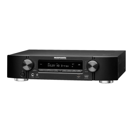
AV Surround Receiver
NR1509
• For purposes of improvement, specifications and design are subject to change without notice.
• Please use this service manual when referring to the operating instructions without fail.
• Some illustrations used in this service manual are slightly different from the actual product.
Service Manual
Click here!
On-line service parts list
http://dmedia.dmglobal.com/Document/DocumentDetails/24507
ONLINE PARTS LIST
(P5)
WEB owner's manual
NA:
http://manuals.marantz.com/NR1509/NA/EN/index.php
EU:
http://manuals.marantz.com/NR1509/EU/EN/index.php
AP:
http://manuals.marantz.com/NR1509/AP/ZH/index.php
Upload is planned for the time of a future press release.
BEFORE SERVICING THIS UNIT
ELECTRICAL
MECHANICAL
REPAIR INFORMATION
UPDATING
Confidential
Ver. 1
Advertisement
Table of Contents

Related Manuals for Marantz NR1509


Summary of Contents for Marantz NR1509
- Page 1 Service Manual Ver. 1 AV Surround Receiver NR1509 Click here! On-line service parts list http://dmedia.dmglobal.com/Document/DocumentDetails/24507 ONLINE PARTS LIST (P5) WEB owner’s manual http://manuals.marantz.com/NR1509/NA/EN/index.php http://manuals.marantz.com/NR1509/EU/EN/index.php http://manuals.marantz.com/NR1509/AP/ZH/index.php Upload is planned for the time of a future press release. BEFORE SERVICING THIS UNIT...
- Page 2 BEFORE SERVICING THIS UNIT SAFETY PRECAUTIONS NOTE FOR SCHEMATIC DIAGRAM HANDLING THE SEMICONDUCTOR AND OPTICS ONLINE PARTS LIST Accessing the Parts List Searching Part Numbers or Ref. Numbers NOTE FOR PARTS LIST SERIAL NUMBER Serial Number Organization SKU Code of this Unit POST-SERVICE PRECAUTIONS Initializing this Unit JIG FOR SERVICING...
-
Page 3: Safety Precautions
SAFETY PRECAUTIONS The following items should be checked for continued protection of the customer and the service technician. Leakage current check Before returning the set to the customer, be sure to carry out either (1) a leakage current check or (2) a line to chassis resistance check. If the leakage current exceeds 0.5 milliamps, or if the resistance from chas- sis to either side of the power cord is less than 460 kohms, the set is defective. -
Page 4: Note For Schematic Diagram
NOTE FOR SCHEMATIC DIAGRAM WARNING: Parts indicated by the z mark have critical characteristics. Use ONLY replacement parts recommended by the manufacturer. CAUTION: Before returning the set to the customer, be sure to carry out either (1) a leakage current check or (2) a line to chassis resistance check. -
Page 5: Note For Parts List
ONLINE PARTS LIST Accessing the Parts List Searching Part Numbers or Ref. Numbers (1) Access from the Service Manual You can search a Parts List for part numbers or Ref. numbers. ・ Click the URL link on the cover of the service manual. (1) Enter the part number or Ref. - Page 6 The 14-digit serial number that contains the code of the manufacturing plant and the manufacturing date. 14 digits Factory Manufactured Cumulative Year, month code code serial number The last Month 2digit of year (01 ~ 12) SKU Code of this Unit Product SKU SKU Code NR1509/U1B NR1509/N1B NR1509/N1SG NR1509/K1B...
-
Page 7: Initializing This Unit
POST-SERVICE PRECAUTIONS Initializing this Unit Make sure to initialize this unit after replacing the microcomputer or any peripheral equipment, or the digital PCB. 1. Press the power button to turn off the power. 2. While holding down buttons "TUNER PRESET CH +" and "INTERNET RADIO" simultaneously, press the power button to turn on the power. -
Page 8: Schematic Diagrams
ELECTRICAL SCHEMATIC DIAGRAMS PRINTED CIRCUIT BOARDS SCH01_MN864787 DIGITAL, F HDMI SCH02_MN864788 SCH03_ADV7623 SPK, SIDE CNT, HDMI GUIDE A, HDMI GUIDE B SCH04_CPU AMP, FRONT, MC HP, USB SCH05_CPU LEVEL CHG REG, GUIDE L, FRONT CNT, REG CNT, SMPS SCH06_DIGITAL CNT SCH07_DIR APLD LEVEL DIAGRAM SCH08_MAIN DAC... - Page 9 SCHEMATIC DIAGRAMS SCH01_MN864787 MN864787 STBY5V FROM CEC5V N1014 D.SUPPLY CEC3.3V VDD33IO CEC1.1V1 L1056 DGND DGND CB05YTYH221 RX_C- RXF_C- RX_C+ RXF_C+ TO 0A DGND RX_0- RXF_0- RX_0+ RXF_0+ DGND L1055 OPEN RX_1- RXF_1- RX_1+ RXF_1+ L1071 DGND CB05YTYH221 RX_2- RXF_2- RX_2+ RXF_2+ DGND DGND...
- Page 10 SCH02_MN864788 MN864788 CEC5V FROM CEC3.3V D.SUPPLY CEC1.1V ADV7623_C- DGND VDD33IO_ ADV7623_C+ L1068 CB05YTYH221 FROM ADV7623_0- TO 6A ADV7623_0+ ADV7623 ADV7623_1- ADV7623_1+ ADV7623_2- TO 8A AVDDH33 ADV7623_2+ L1063 CB05YTYH221 AVDD11 L1057 CB05YTYH221 MN864787_C- MN864787_C+ MN864787_0- MN864787_0+ FROM VDD33 MN864787_1- L1062 CB05YTYH221 VDD11_1 MN864787_1+ MN864787...
- Page 11 SCH03_ADV7623 ADV7623 FROM DV3.3V R1550 312mA DV1.8V R1581 D.SUPPLY DGND FB1000 L1070 OPEN(2012) CB05YTYH221 DV5V DV3.3V_1 40mA L1069 OPEN(2012) DV1.8V_2 TO 4B FB1001 R1579 CB05YTYH221 R1580 FB1002 545mA CB05YTYH221 DV1.8V_1 10UF/16V R1568 R1623 1K-D(1608) 1K-D(1608) R1638 CGND 5V_DETA 1:DDCC_SCL 108:DDCA_SDA 2:CVDD 107:RTERM RXC_C-...
- Page 12 TU_CK AIOS4_GPIO_SPI_EN_A R1204 R1184 TU_DA * OPTION TABLE R1185 TO 2C MN864788_RST TU_LA C1233 100N-K FL_RST MODEL R1206 R1202 R1195 DIR_CE NR1509/U1B OPEN C1234 100N-K R1196 DIR_CLK NR1509/N1B OPEN R1182 AIOS4_STBY_STATUS VEXP_DATA NR1509/K1B R1200 R1181 AIOS4_WAKEUP VEXP_CLK R1180 CPU_POWER VEXP_OE...
- Page 13 SCH05_CPU LEVEL CHG TO 3C TO A4 TO 4C TO A7 CPU LEVEL CHG TO DIGITAL CNT MN864787 MN864788 MAIN DAC STBY3.3V STBY5V FROM SWM3.3V D.SUPPLY M3.3V DGND TO 5C R1091 CEC_COM C1212 OPEN SWM3.3V R1094 CEC_OUT Q1057 R1095 R1096 OPEN OPEN 2SD2114K...
- Page 14 SCH06_DIGITAL CNT DIGITAL CNT TO 7C N1007 D.SUPPLY N1001 H/PR H/P_R H/PGND H/P_GND H/P_L N1001 H/PL C125Z2-23C DAGND2 TO CP4616 AD_IN_L DAC_FL+ DAGND2 DAC_FL- AD_IN_R DAGND DAGND FRONT CNT H3 DAGND2 DAC_FR- AD_VCOM DAC_FR+ DAGND2 DAGND DAGND LEGO_FL CEN+ DAC_C+ DAGND2 DAC_C- CEN-...
- Page 15 SCH07_DIR APLD DIR/A.PLD DIR input DIR output TO 0D TO B8 TO B0 TO 1D TO 2D CH1: DATA CH1:D-DATA FROM FROM NET PHY NET PHY HDMI TX NET PHY CH2: fs CH3: 64fs *FILTER COMPONENTS VALUE TYPE TOLERANCE RT1N141C Q2204 R1907 680 Ω...
- Page 16 SCH08_MAIN DAC TO C4 TO D5 TO D3 TO B7 TO D4 MAIN DAC FROM FROM FROM FROM FROM DIR/A.PLD DIR/A.PLD DIR/A.PLD DA+5V AD_VDCOM ADIN_LEGO_R DAGND2 ADIN_LEGO_L DAGND2 FROM DIGITAL CNT TO C8 C2189 ADIN_VDCOM C2193 A/DIN_L C2188 DAGND2 DAGND2 C2187 A/DIN_R C2185...
- Page 17 SCH09_DSP TO D7 TO D6 TO B6 TO 9D FROM FROM NET PHY DIR/A.PLD DSP1CS DSP1MISO DSP1MOSI DSP1CLK DGND DA3.3V Q2203 RT1N141C 11 12 13 14 15 16 R2119 DSP input DATA I2S(HD Audio) I2S(PCM Multi) DSP1INF/FL I2S0 FL/FR DSP1IN_/FR ----- ----- DTCK...
- Page 18 SCH10_NET PHY TO C2 TO C9 NET PHY FROM DIGITAL_CNT NET3.3V LEGO5V FROM D.SUPPLY NET_I2S2_DOUT NET_I2S2_BCKIN NET_I2S2_DIN NET_I2S2_LRCKIN TO 0E R1331 DGND NET_I2S0_DOUT. R1360 NET_I2S_BCLKOUT. NET_TDM_DOUT R1364 NET_I2S_LRCKOUT. NET_TDM_BCKIN C1190 100N-K NET_TDM_FSIN C1187 100N-K C1882 10N-K R1461 R1462 C1176 1N-K C1024 4.7U-K-1608 19 18 17...
- Page 19 SCH11_D SUPPLY CEC3.3V M3.3V D3.3V2 SWM3.3V DA1.0V DV1.8V NET3.3V DA3.3V DV3.3V D.SUPPLY DGND DGND DGND L1093 CB05YTYH221-2012 L1095 CB05YTYH221-2012 L1092 CB05YTYH221-2012 M3.3V N1033 MN864788 L1138 1.5A N1033 HSFE5040-2.2UH 0-2012 YMW025-06R L1112 CEC1.1V CEC1.1V R1812 R1807 2R7-1608 L1110 0-2012 CEC_POWER RESETOUT R1798 L1104 0-2012...
- Page 20 C4003 47N(M)-50V R4058 0(3216) L4004 SP-2507 D4019 RLY4002 CN4000 LBAS16HT1G R4011 JZC-42F 10(2) C4012 TO CP4800 R4004 10(1/5) NR1509 OPEN C4004 47N(M)-50V * CAPACITOR OPTION 47N(M)-50V C4016-C4020 C4021-C4022 CN4003 U1B/FB/K1B N1SG, N1B U1B/FB/K1B N1SG, N1B 0(3216) R4059 L4005 SP-2507 NR1609 2200PF 0.018UF...
-
Page 21: Side Connector
SCH13_SIDE_CNT SPK_SCNT 2/2 SIDE CONNECTOR TO MX/RC-5 N4600 1.0-11S-4PW OPEN R4638 REMOTE3.3V R4637 MO232I R4636 MI232O M/DGND CLP4010 CP4603 CP4604 HDMI DIGITAL CNT E5 HDMI DIGITAL CNT E3 ON/OFF JACK4602 ZD4700 C4704 PJ-308-02 (BK) ZJ16B 100N-K TO N1001 TO N1003 TRIGGER PJ-308-02 C4705... - Page 22 IN_A6 O_B3 U5200:B DA_FR. DAFR LEGO_AD_R NJM8080G SAT_R IN_B6 *CAP OPTION AGND R5219 C5209 IN_A7 10/50 C5210 100/16-PKR3 DVD_L DA_C. NR1509 NR1609 C5211 100/16-PKR3 DVD_R IN_B7 DA_SW. DASW C5205/C5207/C5210/ TO 3E DATA 47/25_PKR3 100/16_PKR3 AGND PHONO_R C5211/C5212/C5213 C5212 100/16-PKR3 DA_SL.
- Page 23 TO CP4612 VIDEO IN3 VIN5 CN5204 CN5205 C125Z2-21C C125Z2-13C Blu-ray VIN1 R5346 Q5223 VIN_B VIN4 RT1N141C R5347 * MODEL OPTION VIN3 R5348 NR1509 NR1609 VIN2 C5277 C5278 CN5402_21P OPEN INSERT 10/50 100N-K R5349 CN5403_13P INSERT OPEN R5350 VIN_C VIN_A OPTION B...
-
Page 24: Tuner Pack
(CH)3900P-J-1608 R5439 [SL] R5441 R5440 3K9-F-1608 * DAC OPTION C5332 (CH)330P-J-1608 thin_chip R5444 4K7-F-1608 NR1609 NR1509 R5443 / R5444 / R5445 47K-F-1608 4K7-F 6K8-F R5447 / R5453 R5442 / R5445 / DAC OPTION 47K-F 51K-F R5446 / R5454 U5211:B R5448... - Page 25 SCH17_F_HDMI AV 4/4 FRONT HDMI B'D FRONT HDMI (FFC WAFER) R3000 R3001 R3002 R3003 10K-1608 47K-1005 OPEN R3004 OPEN N3000 A111989-G-01-T_W/O_FLNG R3005 OPEN Q3000 RT1N141C .HPA_D.. HP_DET Q3001 RT1N441C DDC_SDA N3001 DDC_SCK N3001 6232-23P ST CE_REMOTE .CEC DGND TXC- D3000 R3006 0*2(AR) LRB521S-30T1G...
- Page 26 SCH18_FRONT NR1609 & NR1509 FRONT B`D R4403 R4410 N/F/K R4409 OPEN R4400 R4410 C4410 OPEN R4403 FIL2 R4401 OPEN R4404 OPEN FIL1 D4400 R4402 OPEN 1N4007 4R7(1) Vkk GND OPEN F500mAL/125V R4416 Q4412 KTC1027Y C4404 ZD4400 10/50 ZJ6.8B C4408 C4411...
- Page 27 SCH19_AMP1 7CH_AMP 1/2 REF : 4800-5199 NR1609, NR1509 AMP B'D 1/2 39.6V R4800 R4802 ZD4800 R4801 R4803 R4804 C4800 ZJ5.1A 100K 5K6(1) PRF18BC471QB5RB 100N-K C4803 Q4800 C4802 47/50_PKR3 TP4800 39.1V C4801 R4805 OPEN R4809 KTA1024Y 10N-K 0.6V 680K 1.1V Q4801...
- Page 28 VR4804 R5003 KSA992F 1K(B)-V R5002 C4871 ZD4814 OPEN 0R22(2) OPEN OPEN R5004 R5005 R5006 D4826 3K3(1) OPEN OPEN NR1609, NR1509 AMP B'D 2/2 R5007 R5008 390K C4873 R5013 C4872 R5009 R5010 R5011 2N2-K Q4845 470P-500V 22(1) 2SB1560 Q4846 R5012 KTC3206Y...
- Page 29 * FUSE OPTION C4143 C4169 ZD4160 ZD4147 ZD4148 ZD4149 ZD4165 R4148 R4149 R4150 R4147 R4152 C4151 C4156 U1B,FB N1SG, N1B, K1B NR1509 NR1609 NR1509 NR1609 F4140 F4141 F4140 F4141 ZJ7.5B ZJ39B ZJ39B ZJ39B ZJ15B 2M2 (5) 2M2 (5) 1M (5) 270K 100/200 0.22/275V...
- Page 30 470/50 1N4148 10/50 1N4148 OPEN 4700/25(MHA) TU +5V 100/16 (KOSHIN) AGND SIDE CONNENCTOR AGND * MODEL OPTION (REG_CNT 2/4 B6) A-8V A+8V NR1509 NR1609 C4605 D4607 ZD4601 C4609 1N4148 OPEN 4700/25(MHA) DA_+5V 100/16 (KOSHIN) OPTION A OPEN INSERT U4603 KIA7908PI...
- Page 31 SCH23_FRONT CNT SMPS_REG_FCNT 3/3 CP4617 HDMI DIGITAL CNT E8 TO N1005 CP4616 * MODEL OPTION TO N1007 NR1509 NR1609 CP4613_23P OPEN INSERT CP4617_15P INSERT OPEN CLP4600 CLP4602 BKT4143 R5371 R5372 C5291 R5367 R5369 U5206:A U5204:A C5286 C5292 C5290 R5363 R5364...
-
Page 32: Lead-Free Solder
When soldering, use the Lead-free Solder (Sn-Ag-Cu). DIGITAL (A SIDE) F HDMI (A SIDE) F HDMI (B SIDE) R1109 R1108 C1020 C1019 C1017 C1018 C1021 R1142 15PIN NR1509 DIGITAL [MP] C1013 C1014 C1016 C1015 R1825 C1012 N1023 C1224 C2138 R1124 C2176 N1014... - Page 33 AV (A SIDE) AV (B SIDE) C5232 C5255 C4223 C4224 C4226 C4217 R4084 C4218 C5312 R5399 R4218 R5385 R5400 R5375 R5380 R4233 R4082 C4227 R5381 R5226 C5289 R5374 CBL/SAT_L CBL/SAT_R C5288 R5225 R5252 R5253 R5331 C5219 C5230 R5272 C5208 C5233 R5391 R5318 R5260...
- Page 34 AC_H AC_L RLY4005 D4007 AC_L JP4000 HF115F/012-2ZS4B CP4001 F4000A F4000B F4000 T6.3AL/250V NR1509 : GBJ1006 CLP4000 CLP4001 NR1609 : GBJ2506 D4006 HDMI_GUIDE_A (A SIDE) SIDE CNT (A SIDE) SIDE CNT (B SIDE) HDMI_GUIDE_B (A SIDE) GASKETTAPE CLP4010 FRONT FFC 3*8 PI12...
- Page 35 AMP, FRONT, MC HP, USB AMP (A SIDE) NR1609 & NR1509 AMP B'D MP R4957 R4966 C4900 R5090 R5091 7020-08221-000-0S C4898 TP4802 C4897 LUG4800 C4884 J4923 R5092 LUG4800 C4823 TP4806 INSERT 23P FFC CABLE TP4808 R5045 R4870 R4881 C4855 CP4801...
- Page 36 REG, GUIDE L, FRONT CNT, REG CNT, SMPS REG (A SIDE) REG (B SIDE) GUIDE L (A SIDE) FRONT CNT (A SIDE) FRONT CNT (B SIDE) JP4631 AD_IN_L AD_IN_L AGND AD_IN_R AGND AGND CN4615 AD_IN_R LEGO_FL CLP4606 AGND LEGO_FL AGND AGND LEGO_FR LEGO_FR...
-
Page 37: Level Diagram
LEVEL DIAGRAM FRONT ch NR1509 LEVEL DIAGRAM FRONT ch NJU72750 NJU72343 ANALOG H/POUT SPEAKER LINE IN + GAIN ADJ. AK4458VN AK5358B + + PREOUT - - to ZONE2 +30dB NJU72343 MAX. OUTPUT 4.2Vrms SP OUT Differential Out 4.48Vrms/8Ω AK4458 MAX SIGNAL LEVEL... - Page 38 CENTER ch NR1509 LEVEL DIAGRAM CENTER ch NJU72343 SPEAKER + GAIN ADJ. AK4458VN + + PREOUT - - +30dB NJU72343 MAX. OUTPUT 4.2Vrms SP OUT Differential Out 4.23Vrms/8Ω AK4458 MAX SIGNAL LEVEL 0dBFS +20dB DOLBY LIMIT LEVEL (ALLch-3dBFS) 0dBFS = +/-2.8Vpp=1.98Vrms...
- Page 39 SUBWOOFER ch NR1509 LEVEL DIAGRAM SUBWOOFER ch NJU72343 SPEAKER + GAIN ADJ. AK4458VN + + PREOUT - - NJU72343 MAX. OUTPUT 4.2Vrms +30dB MAX SIGNAL LEVEL DOLBY LIMIT LEVEL (ALLch-3dBFS) 0dBFS = +/-2.8Vpp=1.98Vrms AK4458 0dBFS +20dB -10dBFS +10dB PREOUT 300mVrms...
- Page 40 SURROUND ch NR1509 LEVEL DIAGRAM SURROUND ch NJU72343 SPEAKER + GAIN ADJ. AK4458VN + + PREOUT - - +30dB NJU72343 MAX. OUTPUT 4.2Vrms SP OUT MAX SIGNAL LEVEL Differential Out 4.23Vrms/8Ω DOLBY LIMIT LEVEL (ALLch-3dBFS) AK4458 +20dB 0dBFS 0dBFS = +/-2.8Vpp=1.98Vrms...
- Page 41 LEGO ADC NR1509 LEVEL DIAGRAM LEGO ADC NJU72750 LINE IN To MAIN To ZONE2 PCM9211 To LEGO +30dB +20dB +20dB PCM9211 0dBFS=1.06Vrms +10dB +10dB -10dBFS LINE IN 200mV -8.5dB -20dBFS A/D IN -10dB -10dB 75.2mVrms (-23.0dBFS) -30dBFS -20dB -20dB -40dBFS...
-
Page 42: Block Diagram
BLOCK DIAGRAM ANALOG AUDIO DIAGRAM NR1509 ANALOG AUDIO DIAGRAM TO DIGITAL AUDIO BLOCK BUFFER INVERTING 7-INPUT/3-OUT MIC(Mini Jack) NJU72750 8-CH VOLUME NJU72343 H/P-L HEADPHONE OUT 7-INPUT/3-OUTPUT NJU72750 InA1 H/P-R 8-CH VOLUME InA2 NJU72343 PHONO_L InA3 OutA1 MAIN_AD_L MAIN_L InA1 OutA... - Page 43 DIGITAL AUDIO DIAGRAM NR1509 DIGITAL AUDIO DIAGRAM ADV7623 HDMI TRANSCEIVER OUT0 MAIN MICOM R5F5631FDDFB TMDS TMDS OUT0 TMDS TMDS HDMI4 TMDS TMDS HDMI5 TMDS OUT1 TMDS HDMI1 HDMI2.0 Matix SW MN864788 TMDS HDMI2 HDMI2.0 RX TMDS HDMI OUT1 Matix SW...
- Page 44 VIDEO DIAGRAM MX25L3206EM2I (4K GUI) NR1509 VIDEO DIAGRAM HDMI4 TMDS IN(4K/60,50HZ/6Gbps) TMDS OUTPUT HDMI5 TMDS IN(4K/60,50HZ/6Gbps) OUT1 TMDS IN(4K/60,50HZ/6Gbps) HDMI1 MN864788 MN864787 Rx/Tx (HDMI2.0 & HDCP2.2) (HDMI2.0 & HDCP2.2) HDMI2 TMDS IN(4K/60,50HZ/6Gbps) TMDS OUTPUT TMDS IN OUT1 OUT0 HDMI3 TMDS IN(4K/60,50HZ/6Gbps)
-
Page 45: Power Diagram
POWER DIAGRAM NR1509 VCC DIAGRAM MAIN +B HI+B LOW+B RELAY S1(AMP +B, -B) MAIN -B LOW-B HI-B RL+B AUDIO+7.0V (Pre) KIA7808API S2(+8V,-8V) KIA7805API KIA7908API AUDIO-7.0V (Pre) OPEN KIA7805API VIDEO+5.0V JUMPER S3(VIDEO) A.TUNER+5.0V KIA7905PI VIDEO-5.0V MAIN TRANS FL AC (F1) S4(VKK) FL AC (F2) DA+5.0V(PCM9211) -
Page 46: Wiring Diagram
WIRING DIAGRAM WiFi_ANT WiFi/BT_ANT DIGITAL PCB MAIN + SPK PCB FRONT CNT PCB AV PCB SMPS PCB REG-CNT PCB REG PCB 7CH AMP PCB FRONT PCB H/P+MIC PCB USB PCB FRONT HDMI PCB PLATE PLATE PLATE... - Page 47 SEMICONDUCTORS Only major semiconductors are shown, general semiconductors etc. are omitted to list. The semiconductor which described a detailed drawing in a schematic diagram are omitted to list. 1. IC's R5F5631FDDFB(DIGITAL_MCU : U1013) Pin Name Symbol Pu/Pd STBY STOP Function STBY P35(IN)/NMI DSP_FLAG0...
- Page 48 Pin Name Symbol Pu/Pd STBY STOP Function Pin Name Symbol Pu/Pd STBY STOP Function STBY STBY HDMI transceiver w/ GUI(ADV7623) control pin (for PE3/AN1 AMPSIGDET Signal level monitor pin (AD converter) PC6/RXD8/IRQ13 HSCL_(400k) DV3VPu HDMI) PE2/RXD12/IRQ7- CURRENT_DET Current level monitor pin (A/D converter) HDMI transceiver w/ GUI(ADV7623) control pin (for DS/AN0 HSDA_(400k)
- Page 49 PCM9211 www.ti.com SBAS495 – JUNE 2010 AD8195 PIN CONFIGURATIONS AD8195ACPZ (AV : U3000) PCM9211 (DIGITAL : U1040) PT PACKAGE LQFP-48 PIN CONFIGURATION AND FUNCTION DESCRIPTIONS (TOP VIEW) ERROR/INT0 VDDRX 30 AVCC PIN 1 30 AVCC NPCM/INT1 RXIN1 29 PE_EN INDICATOR PIN 1 29 PE_EN INDICATOR...
- Page 50 PCM9211 PCM9211 BLOCK DIAGRAM www.ti.com SBAS495 – JUNE 2010 BLOCK DIAGRAM DESCRIPTION NAME FILT TOLERANT AUXIN 0 26 MS/ADR1 Software control I/F, SPI chip select / I2C slave address AUTO RXIN7 setting1(2) RXIN 0 RXIN0 SCKO DOUT RXIN 1 RXIN1 MAIN OUTPUT 27 MODE...
-
Page 51: Pin Description
ADSP21487KSWZ-2B (DIGITAL : U1021) W9864G6KH-6(DIGITAL : U1020) PIN 1 GND PAD (PIN 177) at BOTTOM W9864G6KH TOP VIEW (PINS DOWN) Pin description 5. PIN DESCRIPTION PIN NUMBER PIN NAME FUNCTION DESCRIPTION Multiplexed pins for row and column address. Pin Name Pin No. -
Page 52: Pin Function
AK4458VN 40 +105 C (Exposed pad is connected to ground) 40 +85 C (Exposed pad is open) 48-pin QFN (0.5mm pitch) AKD4458 Evaluation Board for AK4458 AK4458VN (DIGITAL : U1053) Block diagram Pin Configurations CLOCK BUFFER CONTROL SIGNAL GENER ATOR COMMAND DECODER COLUMN DECODER... -
Page 53: Functional Block Diagram
[AK4458] FUNCTIONAL BLOCK DIAGRAM No. Pin Name I/O Function PD State 4. Block Diagram and Functions CAD0_I2C Chip Address 0 Pin in I2C Bus serial control mode Chip Select Pin in 3-wire serial control mode LDOE TVDD VDD18 DVSS AVDD AVSS Hi-Z Audio Data Format Select in Parallel control mode. - Page 54 G Bipolar Technology G Package Outline DIP16,DMP16 I PIN CONFIGURATION and BLOCK DIAGRAM NJU72343 (AV : U5202) NJM2595MTE1 (AV : U5206 Vin1 Vin2 75Ω Vout1 Driver Vin3 Pin Function 75Ω Vout2 No. Symbol Function No. Symbol Function Vin4 Driver AREF Analog reference potential terminal DATA IC control data input...
-
Page 55: Pin Connection
2. FL DISPLAY FLD (CIG25-1801N) (FRONT : U4400) ANODE CONNECTION 17G(AD3) 18G(AD4) SEGA1 SEGA2 SEGA3 SEGA4 SEGA5 SEGA6 SEGA7 SEGA8 SEGA9 SEGA10 SEGA11 SEGA12 SEGA13 SEGA14 SEGA15 SEGA16 SEGA17 SEGA18 SEGA19 SEGA20 SEGA21 SEGA22 SEGA23 SEGA24 SEGA25 SEGA26 PIN CONNECTION SEGA27 SEGA28 SEGA29... - Page 56 For search Function description is located right end. RC-5/ RC-5 Ex. Format Command(*7) AV Receiver AV Receiver Made by: Marantz America, LLC. HDMI Control (CEC) ON 16 84 08 RCRC51608408 HDMI Control(CEC) On HDMI Control (CEC) OFF 16 84 09...
- Page 57 Center - (Down) 16 37 12 RCRC51603712 Center Channel Volume down 3 (PRESET 3) 17 03 RCRC517003 Ten Key 3 ( Pre set No. or Frequency) for Tuner-1 Subwoofer + (Up) 16 37 49 RCRC51603749 Subwoofer channel Volume up 4 (PRESET 4) 17 04 RCRC517004 Ten Key 4 ( Pre set No.
- Page 58 Internet Radio 27 92 20 RCRC52709220 Turn On and select Internet Radio as Zone 2 source Blu-ray(BD) 16 92 12 RCRC51609212 Turn On and select BD SIRIUSXM (*4) 27 92 29 RCRC52709229 M-XPort Turn On and select Sirius XM as Zone 2 source 16 92 13 RCRC51609213 Turn On and select M-XPort...
- Page 59 Need an input assign to the input in Menu in advance the use /U1x version (for North America) model only /N1x version (for Europe) model only /U1x (for North America), /N1x version (for Europe) model only The RC code can be sent using RS-232C/IP Serial protocol commands Revision 14-Mar-18 Added NR1509/NR1609...
- Page 60 MECHANICAL DISASSEMBLY Flowchart 1. FRONT PANEL ASSY 2. RADIATOR ASSY 3. DIGITAL PCB 4. SPK PCB 5. TRANS 6. SMPS PCB 7. REG PCB 8. AV PCB EXPLODED VIEW PACKAGING VIEW...
- Page 61 DISASSEMBLY Flowchart • Remove each part following the flow below. • Reassemble the removed parts in the reverse order. • Read "SAFETY PRECAUTIONS" before reassembling the removed parts. • If wire bundles are removed or moved during adjustment or part replacement, reshape the wires after completing the work. Failure to shape the wires correctly may cause problems such as noise. •...
-
Page 62: Front Panel Assy
• The photographs with no shooting direction indicated were taken from the top of the unit. (1) Remove the screws. • Photos of NR1509 U are used in this manual. The viewpoint of each photograph (Shooting direction : X) [View from the top] ↓Shooting direction: B↓... -
Page 63: Radiator Assy
2. RADIATOR ASSY 3. DIGITAL PCB Proceeding : TOP COVER → RADIATOR ASSY Proceeding : TOP COVER → DIGITAL PCB (1) Remove the screws. (1) Remove the screws. View from the bottom ↑Shooting direction: A↑ (2) Cut the wire clamps, then remove the CORD HOLDERs and connectors. Remove the screws. - Page 64 4. SPK PCB 5. TRANS Proceeding : TOP COVER → DIGITAL PCB → SPK PCB Proceeding : TOP COVER → DIGITAL PCB → TRANS (1) Remove the screws. (1) Remove the CORD HOLDERs and connector wires. from CP4401 ↑Shooting direction: A↑ CP4001 CP4607 (2) Remove the screws.
-
Page 65: Exploded View
EXPLODED VIEW http://dmedia.dmglobal.com/Document/DocumentDetails/24507 Parts List : Ref No.42 : See "PROCEDURE AFTER REPLACING THE U-COM, ETC." NR1509/1609(Marantz) EXPLODE VIEW S 1 - S 9 - 0 9 ) R 1 6 8 ( N 0 9 ) R 1 5 <... - Page 66 PACKAGING VIEW http://dmedia.dmglobal.com/Document/DocumentDetails/24507 Parts List : N R 16 *MANUAL POLYBAG ASSY* *MIC ASSY* POLYBAG CODE: 6337-04006-201-0S POLYBAG CODE: 6330-21071-900-0S POLYBAG CODE: 4148-21019-000-0S ZIPPERBAG(A4size) ZIPPERBAG(A5size) SETUP MIC STAND SIZE : 350mm x 210mm Notes on RADIO (ALL) AWA insertion sheet (F only) This part together with document and zipper bag are supplide.
-
Page 67: Troubleshooting
REPAIR INFORMATION TROUBLE SHOOTING SPECIAL MODE 1. POWER Special mode setting button 2. Analog video 1. Version Display Mode 3. HDMI/DVI 2. PANEL / REMOTE LOCK Selection Mode 4. AUDIO 3-1. Selecting the Mode for Service-related 5. Network / Bluetooth / USB 3-2. - Page 68 TROUBLE SHOOTING 1. POWER 1.1. The unit does not power on 1.2. Fuse is blown The unit does not power on Blown fuse Check for short circuits between the Does the power indicator on the front panel flash Check the rectifier diode in the Does the power shut down after several seconds? Check for leaks and short circuits regulator output terminal and GND...
-
Page 69: Analog Video
: Hi (3.3 V) [N1039 : 14 pin] : Lo (0 V) DIGITAL test point R1109 R1108 N1005 R1142 C1020 C1019 C1017 C1018 C1021 15PIN NR1509 DIGITAL [MP] C1224 C1013 C1014 C1016 C1015 R1825 C1012 N1023 C2138 R1124 C2176 N1014 7020-08228-000-0S... - Page 70 3.1. No picture or sound is output (HDMI to HDMI) No picture or sound is output. (8) When using a MARANTZ Blu-ray/DVD player, is the "HDMI" indicator of the fluorescent display lit? Proceed to YES when using a Blu-ray/DVD player produced by other manufactures.
- Page 71 (15) Are a picture and sound output when a differ- The TV is faulty. ent TV is used? Check the unit. "HDMI "Rx/Tx" Failure Detection"...
-
Page 72: Audio Check
4. AUDIO 4.1. AUDIO CHECK No audio output CHECK 1 INPUT SURROUND MODE SOURCE Check the ANALOG AUDIO BLOCK Audio output OK? ANALOG 2CH DIRECT ANALOG CHECK 2 INPUT SURROUND MODE SOURCE Check the DIGITAL AUDIO BLOCK Legacy Audio output OK? COAX or OPT (PCM or DolbyDigital or dts…) CHECK 3... -
Page 73: Analog Audio
4.2. Power AMP (AMP PCB) 4.3. Analog audio When using the protection pass mode, do not connect speakers to the speaker terminals. No audio output. No audio output. Protection is activated. Is a voltage of ± 8 V supplied to AV PCB [CP5201]? Repair the ±... -
Page 74: Cannot Connect To The Network
5. Network / Bluetooth / USB 5.1. Cannot connect to the network Check the connection environment The circuit of NET5V POWER Insert the LAN cable correctly and then turn on Can the output voltage (5V) to Is NET5V POWER [U1013 : 40pin Is the LAN cable correctly inserted? between [U1013-Q1083 : FET- the power again. - Page 75 5.2. Cannot establish a Bluetooth connection Check the Bluetooth device being used Are the versions of the HEOS Version displayed in The Network Module software is faulty. Version Check Mode? Is the Bluetooth device compatible with the A2DP Use a device that is A2DP profile compatible. profile? The circuit of Network Module is faulty.
- Page 76 5.3. Cannot recognize the connected USB device 5.4. No picture or sound is output Check the USB device being used Checking the unit (If no picture is output) Are digital video signals(LEGOPCK, LEGOVS, The circuit around Network Module, [U1024 : Is a USB hub being used? Do not use a USB hub.
- Page 77 DIGITAL test point USB test point R1109 R1108 C1020 C1019 C1017 C1018 C1021 R1142 15PIN NR1509 DIGITAL [MP] C4442 C1013 C1014 C1016 C1015 R1825 C1012 N1023 C1224 C2138 R1124 C2176 CP4402 N1014 7020-08228-000-0S C2178 15PIN C2177 N1033 CP4402 SN74LVC244APWR N1021...
- Page 78 6. SMPS Operation waveform for each part DC 5V is not output. After primary side rectification Primary drain (Caution: High voltage, electric shock) (Caution: High voltage, electric shock) OPTION OPTION OPTION_2 Replace the [U4140 : TOP268VG Is [U4140 : TOP268VG] dam- and D4142 / D4143 / D4144 / After secondary rectifications aged?
- Page 79 HDMI "Rx/Tx" Failure Detection 1. Prior checking Check item(0). Checking the HDMI connector Checking the condition of the HDMI pin (rear/front). There are deformed pins. Replace the HDMI connector. Check for deformed pins. None of the pins are deformed. Check by following the flow chart for "3.
- Page 80 Stop bits: 1 Parity: none Transmitted text S706-709 : No Preference S702 : 3.3V Flow control: none Select Append CR-LF Forward: (none) Check the Local Echo check box. Figure 1 Device Connection Method (NR1509) Figure 3 Serial Port Setup Screen...
-
Page 81: Indicator Lights
After exiting "Setup Assistant" execute the above. 1. Input a command in the Press 2.Click on the transmission button. transmission command input. Figure 6-1. AVR settings (NR1509) All the for Volume 7 segment indicator Lights Figure 8. Method for Sending Termite Commands... -
Page 82: Contact Support
3. Starting detecting the point of failure Check item(1). (2-2) Display when an Error is not detected. Check the power supply status and communication status with the CPU of each device. Start in HDMI Diagnostics mode and follow the procedures below. 1 Auto Test Cancel the mode, and proceed to check item... - Page 83 Check item(2). : Check operation of the HDMI input terminal. Check item(3). : Check operation of the HDMI output terminal. Go to check item (52) (OSD [ADV7623] failure detection When the HDMI input terminal of this device is connected to the player correctly, is sound heard from procedure) the speaker? ※...
- Page 84 3-1. Error Code H1-01 failure detection procedure Checking device. (HDMI Rx/Tx) Check the power supply voltage. (HDMI Rx/Tx) Checking the reset waveform. (HDMI Rx/Tx) Check item(5). Check the power supply voltage. : Check item(7). Checking the reset waveform : Check the waveform. Does the power supply voltage of the HDMI Rx/Tx [U1027] indicate the correct voltage (1.1V, 3.3V)? When the power is turned on, is the TP waveform correct (as The test points are as follows.
- Page 85 Check the I2C communication line. (HDMI Rx/TX) Check item(8). Check the I2C communication line : Check the CPU. Is the "I2C" waveform of the TP HDMI Rx/Tx [U1027] correct (like the one shown in the diagram) when the power is turned P_DA 116pin P_CK 114pin U1027...
- Page 86 3-2. Error Code H1-02 failure detection procedure Checking device. (HDMI SW) Checking the reset waveform. (HDMI SW) Check item(10). Checking the reset waveform : Check the waveform. When the power is turned on, is the TP waveform correct (as shown in the figure)? Examples of confirmation waveform 115 pin Voltage scale:1.0V/div...
- Page 87 3-3. Error Code H1-07 failure detection procedure Checking device. (OSD) Check the power supply voltage. Checking the reset waveform. Check item(14). Checking the reset : Check item(12). Check the power supply voltage. Check item(13). Check the power supply voltage. Check the CPU. Does the power supply voltage of the OSD Check the power supply components [U1067,...
- Page 88 Check the I2C communication line. Check item(15). Check the I2C communication line : Check the CPU. Is the "I2C" waveform of the HDMI OSD [U1030] correct (like the one shown in the diagram) when the power is turned on? HSCL HSDA U1030 *The diagram shows an example.
- Page 89 3-4. Error Code H1-15 failure detection procedure Checking device. [U1029 : MX25L3206EMI(U, K, F)/MX25L6406EMI(N)] Check item(17). Write to the OSD ROM. Recheck from check item (1). Does Error Code H1-15 continue? Check item(18). Replace [U1029] with a new device. Recheck from check item (1).
- Page 90 3-5. Error Code H1-08 failure detection procedure Checking device. [U1021 : ADSP21487] Check the power supply voltage. Checking the reset waveform. Check item(19). Check the power supply voltage. Check item(20). Check the power supply voltage. Check item(21). Checking the reset : Check the CPU.
- Page 91 Check the SPI communication line. Check item(22). Check the SPI communication line : Check the CPU. Is the "SPI" waveform of the TP near the DSP [U1021] correct (like the one shown in the diagram) when the power is turned on? D_CK 3pin D_MOSI 4pin D_CS 6pin...
- Page 92 3-6. Error Code H1-12 failure detection procedure Checking device. [U1040 : PCM9211] Check the power supply voltage. Checking the reset waveform. Check item(24). Check the power supply voltage. Check item(25). Check the power supply voltage. Check item(26). Checking the reset : Check the CPU.
- Page 93 Check the communication line. Check item(27). Check the communication line : Check the CPU. Is the waveform of the TP near the DIR [U1040] correct (like the one shown in the diagram) when the power is turned on? DR_CK 25pin DR_DIN 24pin DR_CE 26pin DR_DOUT 23pin...
- Page 94 3-7. HDMI Rx/Tx [MN864788] failure detection procedure Checking operation between the HDMI Rx/Tx device and the player Check item(30). Checking the DDC status register : Example Send the following command from Termite.exe. b In order to check, connect the player to the HDMI terminal and configure the player as AVR source. Check the sound output while turning on the player.
- Page 95 When the results of check item (29) are "00" When the results of check item (30) are "00 or 04" (Detection of 5V is not OK) (Detection of DDC is not OK.) Check the +5V voltage. (HDMI Rx/TX) Check the DDC line. (HDMI Rx/Tx) Check item(31).
- Page 96 When the results of check item (30) are "22" (Detection of DDC is OK.) Checking the TMDS status register 3.3V TMDS Signal TMDS Check item(33). Checking register of the TMDS CLK detection status Example register : Example of waveform in check ① Example of waveform in check ② Send the following command from Termite.exe.
- Page 97 3-8. HDMI SW [MN864787] failure detection procedure Checking operation between the HDMI (HDMI SW) device and the player HDMI IN Check item(37). Checking the DDC status register : Example Send the following command from Termite.exe. Case of HDMI IN1 b In order to check, connect the player to the HDMI terminal and configure the player as AVR source. Send the command "i 002B 0084 0001".
- Page 98 When the results of check item (36) are "00" When the results of check item (37) are "00 or 04" (Detection of 5V is not OK) (Detection of DDC is not OK.) Check the +5V voltage. (HDMI SW) Check the DDC line. (HDMI SW) Check item(38).
- Page 99 When the results of check item (37) are "22" (Detection of DDC is OK.) Checking the TMDS status register (HDMI SW) 3.3V TMDS Signal TMDS Check item(40). Checking register of the TMDS CLK detection status Example register : Example of waveform in check ① Example of waveform in check ② Send the following command from Termite.exe.
- Page 100 3-9. Front HDMI Buffer IC [AD8195] failure detection procedure Checking operation between the HDMI (Front HDMI Buffer) and the player Checking the +5V/DDC status register (Front HDMI Buffer) Check item(46). Checking the 5V status of the register : Example Send the following command from Termite.exe. b In order to check, connect the player to the HDMI terminal and configure the player as AVR source.
- Page 101 When the results of check item (46) are "00" When the results of check item (47) are "00 or 04" (Detection of 5V is not OK.) (If the DDC are not OK) Check the +5V voltage. (Front HDMI Buffer) Check the DDC Line. (Front HDMI Buffer) less than 100KHz Check item(48).
- Page 102 When the results of check item (47) are "22" (Detection of DDC is OK) Checking the TMDS status register 3.3V TMDS Signal Check item(50). Check the TMDS CLK detection status of the register Check item(51). Checking the TMDS input waveform. : Example Check the TMDS waveform at the following test point.
- Page 103 3-10. OSD [ADV7623] failure detection procedure Checking the TMDS status register (OSD -> HDMI Rx/Tx) 3.3V TMDS Signal Check item(52). Check the TMDS CLK detection status of the register Check item(53). Checking the TMDS input waveform. : Example Check the TMDS waveform at the following test point. Send the following command from Termite.exe.
- Page 104 Check the connection between the HDMI OUT terminal and the TV. Connect the HDMI OUT terminal and the TV, and then turn on the TV and check the following items. Checking the HPD/RXSENSE status register. (HDMI TX -> Monitor) Check item(54). Check the HPD and RXSENSE register value of the Example HDMI TX device.
- Page 105 When the results of check item (54) are "03" (Detection of HPD is OK / Detection of RXSENSE is OK ) Example Checking the EDID register. (Monitor) Check item(55). Check the Monitor EDID : ① Unplug the AC cord. Plug the AC cord into a power outlet. ②...
- Page 106 When the results of check item (54) are "01" When the results of check item (54) are "02" (Detection of HPD is OK / Detection of RXSENSE is not OK ) (Detection of HPD is not OK / Detection of RXSENSE is OK ) Check the RXSENSE.
- Page 107 When the results of check item (54) are "00" (Detection of HPD is not OK / Detection of RXSENSE is not OK ) Check the RXSENSE/HPD. (Monitor) Check item(60). Checking the HPD and RXSENSE. : Does the test point of RXSENSE close to the HDMI output terminal [N1018] indicate the (3.3V)? Does the voltage of HPD test point close to the HDMI output terminal [N1018] indicate "Hi"...
- Page 108 3-11. Fault detection procedure between HDMI Rx/Tx [MN864788] & OSD [ADV7623]. HDMI IN1 HDMI OUT ※ In order to check, connect the player to the HDMI terminal and configure the player and TV as AVR source. Check the sound output while turning on the player and TV. Checking the TMDS status register (Rx/Tx ->...
- Page 109 4. Device implementation location DIGITAL (A SIDE) F-HDMI (A SIDE) R1109 R1108 C1020 C1019 C1017 C1018 C1021 R1142 R1825 C1012 15PIN NR1509 DIGITAL [MP] C1224 C1013 C1014 C1016 C1015 N1023 C2138 R1124 C2176 N1014 7020-08228-000-0S N1014 C2178 15PIN C2177 N1033...
-
Page 110: Clock Flow & Wave Form In Digital Block
DATADIR1 U1040 SDTO PLDADCDATA PCM9211 FSDIR1 DAC input 64FSDIR1 R1903 R1109 R1108 R1142 C1020 C1019 C1017 C1018 C1021 15PIN NR1509 DIGITAL [MP] C1224 C1013 C1014 C1016 C1015 R1825 C1012 N1023 C2138 R1902 R1124 C2176 N1014 7020-08228-000-0S C2178 CH1: DATA 15PIN... -
Page 111: Special Mode Setting Button
SPECIAL MODE Special mode setting button b No. 1 - 4, 6 - 8 : While holding down buttons "A", "B" and "C" simultaneously, press the power button to turn on the power. b No. 5, 9, 10 : While the power is on, hold down buttons "A" and "B" for at least 3 seconds . Mode Button A Button B Button C Descriptions... - Page 112 Q3 HEOS Module : Q8 Wi-Fi MAC Address : q Model destination information : y DSP ROM : HEOS Module *Wi-Fi MAC NR1509 \ :**.** "Press "STATUS" button. "Press "STATUS" button. \ : Region (U, N, K, F) ******-****** u Audio PLD : w Serial Number : Audio PLD:**.**...
-
Page 113: Error Display
1.4. Error display See the table below for descriptions of the displayed errors and countermeasures for these. If multiple errors occur, only one item is displayed. The priority order is w, e, r, q. Condition States Display TROUBLE SHOOTING • Check the resistor for setting the region [R1202, 1206, DIGI- FIRM ERROR TAL PCB]. - Page 114 1.5. Version Display in the Setup Menu Follow the steps below to display the firmware information. (1) Press the "SETUP" button on the remote control. (2) Select "General - Information - Firmware". The version information is displayed as a 16-digit number as shown in the screenshot below. General/Firmware Version XXXX-XXXX-XXXX-XXXX...
- Page 115 2. PANEL / REMOTE LOCK Selection Mode 2.1. Actions Switch the PANEL LOCK and REMOTE LOCK modes between on and off. 2.2. Starting up While holding down buttons "M-DAX" and "DIMMER" simultaneously, press the power button to turn on the power. Select the desired mode using the "TUNER PRESET CH+"...
-
Page 116: Service Check
3-1. Selecting the Mode for Service-related 3-1.1. Actions Select diagnostic mode (service path check mode), protection history display mode, or Operation Info 4.OP INFO mode or TUNER STEP mode. Operation Info for the unit can be checked. 3-1.2. Starting up While holding down buttons "TUNER PRESET CH+"... -
Page 117: Protection History Display Mode
3-2. Protection History Display Mode 3-2.1. Actions (3) DC (if the last protection is DC) This mode enables the unit to record and display the event when the THERMAL, ASO or DC protection is PRT:DC activated. Cause : DC output of the power amplifier is abnormal. If protections have been activated multiple times, the latest protection operation is recorded. - Page 118 3-2.4. Clearing the Protection History There are two ways to clear the protection history. (1) Activate Protection History Display Mode. Press the "STATUS" button to display the protection history. Press and hold the "DIMMER" button for 3 seconds. PRT:DC Press and hold the "DIMMER" button for 3 seconds. PRT:CLEAR The above message is displayed and the protection history is cleared.
- Page 119 3-3. Operation Info Mode 3-4. TUNER STEP mode (U / N only) 3-3.1. Actions 3-4.1. Actions This mode enables the unit to display the accumulated operating time, power On count and each This is a special mode for enabling reception STEP of the ANALOG TUNER to be changed. protection count.
-
Page 120: Network Initialization Mode
4. Protection Pass Mode 5. Network Initialization Mode 4.1. Actions 5.1. Actions • This mode allows the power to be turned on without activating protections. The following items are initialized. • This mode functions in the same way as normal power-on, except that protections are not activated. Network setup •... -
Page 121: Product Mode
6. Clearing the Operation Info 7. Log Capture feature 6.1. Actions 7.1. Actions • Displays the accumulated operating time of the unit, the number of times the power was switched on, • Acquires the Network Module log. and the number of occurrences of each protection. •... - Page 122 DIAGNOSTIC MODE Service Path Check Mode 1.1. Actions This function is convenient for confirming problem paths in the product and checking the paths after repairing. The Video and Audio paths can be checked. The backup data is not rewritten. 1.2. Starting up While holding down buttons "TUNER PRESET CH+"...
- Page 123 1.6. Confirmation items for the video system See the block diagram fig.VXXth. Paths to be confirmed Display Settings What to confirm Input Source : CBL/SAT ・ CVBS input ⇒ CVBS output Video Conversion (IP Scaler) : OFF, All sources ( b The input source can be switched to any source except CBL/SAT.) 1 Analog Video pass fig.V01 V01:VIDEO PASS...
-
Page 124: Diagnostic Path Diagram
DIAGNOSTIC PATH DIAGRAM fig.A01 NR1509 ANALOG AUDIO DIAGRAM TO DIGITAL AUDIO BLOCK BUFFER INVERTING 7-INPUT/3-OUT MIC(Mini Jack) NJU72750 8-CH VOLUME NJU72343 H/P-L HEADPHONE OUT 7-INPUT/3-OUTPUT InA1 NJU72750 H/P-R 8-CH VOLUME InA2 NJU72343 PHONO_L InA3 OutA1 MAIN_AD_L MAIN_L InA1 OutA TUNER_L... - Page 125 NR1509 DIGITAL AUDIO DIAGRAM ADV7623 HDMI TRANSCEIVER OUT0 MAIN MICOM R5F5631FDDFB TMDS TMDS OUT0 TMDS TMDS HDMI4 TMDS TMDS HDMI5 TMDS OUT1 TMDS HDMI1 HDMI2.0 Matix SW MN864788 TMDS HDMI2 HDMI2.0 RX TMDS HDMI OUT1 Matix SW OUT1 MN864787...
- Page 126 NR1509 ANALOG AUDIO DIAGRAM TO DIGITAL AUDIO BLOCK BUFFER INVERTING 7-INPUT/3-OUT MIC(Mini Jack) NJU72750 8-CH VOLUME NJU72343 H/P-L HEADPHONE OUT 7-INPUT/3-OUTPUT InA1 NJU72750 H/P-R 8-CH VOLUME InA2 NJU72343 PHONO_L InA3 OutA1 MAIN_AD_L MAIN_L InA1 OutA TUNER_L DA_FL LEGO_AD_L InA4...
- Page 127 NR1509 DIGITAL AUDIO DIAGRAM ADV7623 HDMI TRANSCEIVER OUT0 MAIN MICOM R5F5631FDDFB TMDS TMDS OUT0 TMDS TMDS HDMI4 TMDS TMDS HDMI5 TMDS OUT1 TMDS HDMI1 HDMI2.0 Matix SW MN864788 TMDS HDMI2 HDMI2.0 RX TMDS HDMI OUT1 Matix SW OUT1 MN864787...
- Page 128 NR1509 ANALOG AUDIO DIAGRAM TO DIGITAL AUDIO BLOCK BUFFER INVERTING 7-INPUT/3-OUT MIC(Mini Jack) NJU72750 8-CH VOLUME NJU72343 H/P-L HEADPHONE OUT 7-INPUT/3-OUTPUT InA1 NJU72750 H/P-R 8-CH VOLUME InA2 NJU72343 PHONO_L InA3 OutA1 MAIN_AD_L MAIN_L InA1 OutA TUNER_L DA_FL LEGO_AD_L InA4...
- Page 129 NR1509 DIGITAL AUDIO DIAGRAM ADV7623 HDMI TRANSCEIVER OUT0 MAIN MICOM R5F5631FDDFB TMDS TMDS OUT0 TMDS TMDS HDMI4 TMDS TMDS HDMI5 TMDS OUT1 TMDS HDMI1 HDMI2.0 Matix SW MN864788 TMDS HDMI2 HDMI2.0 RX TMDS HDMI OUT1 Matix SW OUT1 MN864787...
- Page 130 NR1509 ANALOG AUDIO DIAGRAM TO DIGITAL AUDIO BLOCK BUFFER INVERTING 7-INPUT/3-OUT MIC(Mini Jack) NJU72750 8-CH VOLUME NJU72343 H/P-L HEADPHONE OUT 7-INPUT/3-OUTPUT InA1 NJU72750 H/P-R 8-CH VOLUME InA2 NJU72343 PHONO_L InA3 OutA1 MAIN_AD_L MAIN_L InA1 OutA TUNER_L DA_FL LEGO_AD_L InA4...
- Page 131 MX25L3206EM2I (4K GUI) NR1509 VIDEO DIAGRAM TMDS IN(4K/60,50HZ/6Gbps) HDMI4 TMDS OUTPUT HDMI5 TMDS IN(4K/60,50HZ/6Gbps) OUT1 HDMI1 TMDS IN(4K/60,50HZ/6Gbps) MN864788 MN864787 Rx/Tx (HDMI2.0 & HDCP2.2) (HDMI2.0 & HDCP2.2) TMDS IN(4K/60,50HZ/6Gbps) HDMI2 TMDS OUTPUT OUT1 TMDS IN OUT0 HDMI3 TMDS IN(4K/60,50HZ/6Gbps)
- Page 132 MX25L3206EM2I (4K GUI) NR1509 VIDEO DIAGRAM TMDS IN(4K/60,50HZ/6Gbps) HDMI4 TMDS OUTPUT HDMI5 TMDS IN(4K/60,50HZ/6Gbps) OUT1 HDMI1 TMDS IN(4K/60,50HZ/6Gbps) MN864788 MN864787 Rx/Tx (HDMI2.0 & HDCP2.2) (HDMI2.0 & HDCP2.2) TMDS IN(4K/60,50HZ/6Gbps) HDMI2 TMDS OUTPUT OUT1 TMDS IN OUT0 HDMI3 TMDS IN(4K/60,50HZ/6Gbps)
- Page 133 MX25L3206EM2I (4K GUI) NR1509 VIDEO DIAGRAM TMDS IN(4K/60,50HZ/6Gbps) HDMI4 TMDS OUTPUT HDMI5 TMDS IN(4K/60,50HZ/6Gbps) OUT1 HDMI1 TMDS IN(4K/60,50HZ/6Gbps) MN864788 MN864787 Rx/Tx uCOM (HDMI2.0 & HDCP2.2) (HDMI2.0 & HDCP2.2) TMDS IN(4K/60,50HZ/6Gbps) HDMI2 TMDS OUTPUT OUT1 TMDS IN OUT0 HDMI3 TMDS IN(4K/60,50HZ/6Gbps)
- Page 134 NR1509 DIGITAL AUDIO DIAGRAM ADV7623 HDMI TRANSCEIVER OUT0 MAIN MICOM R5F5631FDDFB TMDS TMDS OUT0 TMDS TMDS HDMI4 TMDS TMDS HDMI5 TMDS OUT1 TMDS HDMI1 HDMI2.0 Matix SW MN864788 TMDS HDMI2 HDMI2.0 RX TMDS HDMI OUT1 Matix SW OUT1 MN864787...
- Page 135 NR1509 ANALOG AUDIO DIAGRAM TO DIGITAL AUDIO BLOCK BUFFER INVERTING 7-INPUT/3-OUT MIC(Mini Jack) NJU72750 8-CH VOLUME NJU72343 H/P-L HEADPHONE OUT 7-INPUT/3-OUTPUT InA1 NJU72750 H/P-R 8-CH VOLUME InA2 NJU72343 PHONO_L InA3 OutA1 MAIN_AD_L MAIN_L InA1 OutA TUNER_L DA_FL LEGO_AD_L InA4...
- Page 136 NR1509 DIGITAL AUDIO DIAGRAM ADV7623 HDMI TRANSCEIVER OUT0 MAIN MICOM R5F5631FDDFB TMDS TMDS OUT0 TMDS TMDS HDMI4 TMDS TMDS HDMI5 TMDS OUT1 TMDS HDMI1 HDMI2.0 Matix SW MN864788 TMDS HDMI2 HDMI2.0 RX TMDS HDMI OUT1 Matix SW OUT1 MN864787...
- Page 137 MX25L3206EM2I (4K GUI) NR1509 VIDEO DIAGRAM TMDS IN(4K/60,50HZ/6Gbps) HDMI4 TMDS OUTPUT HDMI5 TMDS IN(4K/60,50HZ/6Gbps) OUT1 HDMI1 TMDS IN(4K/60,50HZ/6Gbps) MN864788 MN864787 Rx/Tx (HDMI2.0 & HDCP2.2) (HDMI2.0 & HDCP2.2) TMDS IN(4K/60,50HZ/6Gbps) HDMI2 TMDS OUTPUT OUT1 TMDS IN OUT0 HDMI3 TMDS IN(4K/60,50HZ/6Gbps)
-
Page 138: Jig For Servicing
JIG FOR SERVICING Use the following jigs (extension cable kit) when repairing the PCBs. (3) Remove the DIGITAL PCB from the chassis and turn it over. Order with your dealer for the jigs your dealer if necessary. Place an insulation sheet larger than the PCB underneath the DIGITAL PCB. b Connect the earth of the PCB to the chassis using an earth wire, etc. -
Page 139: Adjustment Procedure
ADJUSTMENT Adjusting Idling Current NOTE: Adjusting the idling current when "ECO Mode" is set may damage the Power AMP. 1. Preparation (1) Prepare a DC voltmeter. AMP UNIT (2) Place the unit under normal usage conditions, away from highly ventilated areas such as next to an air conditioning machine or electric fan. - Page 140 UPDATING PROCEDURE AFTER REPLACING THE PCB. PROCEDURE AFTER REPLACING THE U-COM, ETC. FIRMWARE UPDATE PROCEDURE 1. Items necessary for update 2. Updating via USB 3. Update method when the DIGITAL PCB or network module is replaced (Using a USB flash drive) 4.
- Page 141 SOFTWARE : PIMG ROM R1109 R1108 C1020 C1019 C1017 C1018 C1021 R1142 C1013 C1014 C1016 C1015 R1825 C1012 N1023 15PIN NR1509 DIGITAL [MP] C1224 C2138 R1124 C2176 N1014 7020-08228-000-0S C2178 MODULE NETWORK MODULE SOFTWARE : Network 15PIN C2177 N1021 N1033 Q1026 Q1037...
-
Page 142: Firmware Update Procedure
Update download file when the firmware is updated (Two files, "HW component" and "LEGO component") Download from SDI Model Name Model Area For HW component For LEGO component NR1509 U North America (U) Product ID : 100100650100 DPMS_NR1509U_LEGO_xxxx.zip NR1509 N Europe (N) Product ID : 100100650200 DPMS_NR1509N_LEGO_xxxx.zip... -
Page 143: Updating Via Usb
2. Updating via USB The latest firmware can be downloaded to a USB memory for updates. 2.1. Connecting to the USB Memory (1) Preparation • Use a memory that supports USB2.0. • USB format : Prepare a USB memory formatted in FAT16 or FAT32. •... - Page 144 3. Update method when the DIGITAL PCB or network module is replaced (Using a USB flash drive) 3.1. File structure on USB flash drive (5) USB Update starts automatically. The Standby LED lights red. DIGITAL PCB or network module is replaced onto the USB flash drive in the following structure. Display during USB update After unzipping the files, store them in the root of the same USB flash drive.
- Page 145 4. Update Method for Service Region Settings Copy the Service Region Settings from the USB flash drive to this unit. (5) Copy the files created on the USB flash drive. 4.1. Creating a Service Region Settings file (1) Click [Start button] - [Accessories] - [notepad] on the PC to launch the notepad. copy to USB flash drive (2) Enter "TEXT".
- Page 146 5. Normal Firmware Update Method from USB Flash Drive 5.1. File structure on USB flash drive (4) Insert the USB flash drive into the USB port. Copy the normal update files onto the USB flash drive in the following structure. Download firmware After unzipping the HW component USB update files for the target model and LEGO USB update files, in USB flash drive.
-
Page 147: Network Connection
6. Normal Firmware Update Method from OTA 6.2. Check and update the firmware Download the latest firmware from our website and update the firmware. 6.1. Network Connection Check if there is a firmware update available. It is also possible to check approximately how long the (1) System Requirements update will take. - Page 148 : DeviceID, Update ErrorYYXX : ErrorCode) Update ErrorYYXX DSP2 ↓↑ The display is alternately displayed. b Except : NR1509/NR1609/SR5013 DSP3 Please check you b Except : NR1509/NR1609/SR5013 Content of the display is scrolled. DSP4 b Except : NR1509/NR1609/SR5013 Audio PLD...
- Page 149 Copyright © 2018 D&M Holdings Inc. All Rights Reserved.
Need help?
Do you have a question about the NR1509 and is the answer not in the manual?
Questions and answers