Table of Contents
Advertisement
Quick Links
RA9530-R
Evaluation Kit
The RA9530-R-EVK Wireless Power Evaluation
Board can demonstrate the features and
performance of the RA9530 Wireless Power
Receiver with WattShare™ mode. The board comes
with pre-programmed reference firmware in which
GPIOs are configured for specific functions that meet
broader customer requirements.
The RA9530 features Multiple-Time Programmable
(MTP) non-volatile memory that enables customers
to customize the design parameters such as default
output voltage and FOD thresholds. The RA9530
includes over-temperature and voltage protection.
Fault conditions associated with power transfer are
managed by an industry-leading 32-bit ARM
®
Cortex
-M0 processor offering a high level of
programmability while consuming low standby power.
The RA9530 Windows Graphical User Interface
(GUI) can be used to configure the design
parameters, monitor operating parameters such as
Rectifier voltage, and program the new configuration
into the RA9530.
The RA9530-R-EVK is designed for evaluation
purposes only. It must not be used for module or
mass production purposes.
Evaluation Kit Contents
■
RA9530-R Demo Board assembled with coil
R16UH0022EU0200 Rev.2.00
Jul 22, 2022
Features
■
Delivers up to 30W of power in Renesas high
power mode when paired with P9247-GB-EVK
■
±1.5% accurate output current sensing for robust
FOD detection
■
WattShare
capability
■
Supports latest WPC 1.3 specification
■
Supports bi-directional data communications
■
90% peak efficiency (system end-to-end)
■
Switch mode PCLAMP/ECLAMP for robust
overvoltage clamping
®
■
Embedded 32-bit ARM
■
32kB EEPROM memory to support OTA updates
■
Easy to use GUI for customizing the design
parameters
■
1.2V and multiple other IO voltage rail support to
interface with processors of advanced technology
nodes
■
RA9530 Device Package: 6 × 8 ball array, 2.53 ×
3.31 × 0.60 mm, 48-DSBGA with 0.40mm ball
pitch
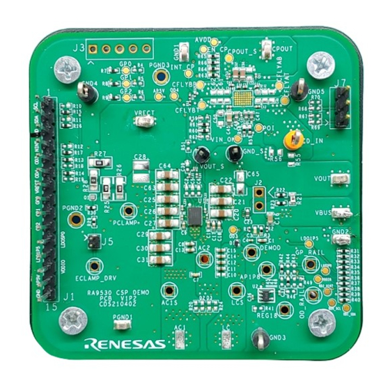
Evaluation Board
SCL
SDA
GND
RA9530
J1 Test
Connector
TM
TRx mode with up to 10W Tx
TM
®
Cortex
-M0 processor
© 2022 Renesas Electronics
Manual
VRECT
VOUT
Page 1
Advertisement
Table of Contents

Related Manuals for Renesas RA9530-R


Summary of Contents for Renesas RA9530-R
- Page 1 The RA9530-R-EVK Wireless Power Evaluation Board can demonstrate the features and ■ Delivers up to 30W of power in Renesas high performance of the RA9530 Wireless Power power mode when paired with P9247-GB-EVK Receiver with WattShare™ mode. The board comes ■...
-
Page 2: Table Of Contents
Wattshare TRx Mode Input Voltage ..................18 TRx Mode Auto-Enable ......................18 TRx System Efficiency ......................19 RA9530-R-EVK Evaluation Board Test Point and Connector ..............19 RA9530-R-EVK Evaluation Board Test Point Placement ..............19 J3 Dongle Connector Pin Descriptions ................. 19 J1 Test Connector Pin Descriptions .................. - Page 3 RA953-R Evaluation Kit Manual Input Capacitor (VRECT Capacitors) ......................31 Output Capacitor (VOUT Capacitors) ......................31 10. LDO1P5 Capacitor ............................31 11. LDO5P0 Capacitor ............................31 12. PCLAMP Connection ........................... 32 13. GPIO Pins ..............................32 OD0/SCL Pin ............................33 OD1/SDA Pin ............................
- Page 4 RA953-R Evaluation Kit Manual Iout Value Register (0x0044, 16-Bit) ..................59 System Command Register (0x004E, 16-Bit) ............... 59 Proprietary Data-Out Registers (0x0050 - 0x0057, 8 Bytes) ..........60 Proprietary Data-In Registers (0x0058 - 0x005F, 8 Bytes) ........... 60 ILIM Register (0x0060, 8-Bit) ....................60 Over Voltage Register (0x0061, 8-Bit) ..................
- Page 5 RA953-R Evaluation Kit Manual TX Status Register (0x007E, 8-Bit) ..................... 74 Vin Value Register (0x0080, 16-Bit) ....................74 Vrect Value Register (0x0082, 16-Bit) ....................74 Die Temperature Value Register (0x0084, 16-Bit) ................74 CEP Value Register (0x00A5, 8-Bit) ....................74 Rx Manufacturer Code Register (0x00B0, 16- Bit) ................
- Page 6 Figure 21. USB to I2C Dongle Header of “USB-FTDI-V2-1”(FTDI) Dongle............21 Figure 22. USB to I2C Dongle Header of “WPD-USB- DONGLE”................. 21 Figure 23. USB-I2C Bridge Connected to I2C Terminal J1 of RA9530-R EVK Board ........... 21 Figure 24. Initial Screen of RA9530-R GUI ......................22 Figure 25.
-
Page 7: Board Setup
Complete the following procedures to install the software: 1. Do not connect the WPD-USB-DONGLE dongle before installing the software. 2. Run the RA9530-R Windows GUI exe file. If you encounter a USB driver issue, please complete the following steps. a. Run the downloaded USB Drivers Setup executable file and follow the user prompts to install the USB drivers. -
Page 8: Usage Guide
Figure 2. Evaluation Kit Connections for Rx Mode Test Start Guide for Rx Operation Place the bottom side of RA9530-R EVK onto an P9247-GB-EVK (REA High power mode enabled Tx) or P9243- GB-EVK (EPP transmitter with fast charge modes) or other WPC certified Tx unit. The RA9530-R-EVK includes a 55 ×... -
Page 9: Rx Start Up
3. Trigger oscilloscope sweep on VRECT, VOUT and AC1 test point when Rx starts up. Figure 3. Rx Start Up Modulation Waveform RA9530-R modulates Rx AC signal with communication capacitor to send ASK packet to Tx. Figure 4. ASK Modulation Signal on CM1 and CM2 R16UH0022EU0200 Rev.2.00... -
Page 10: Load Step
RA953-R Evaluation Kit Manual Load Step The procedure for load step is as follows 1. Set up the Tx as described in section 1.4. 2. Provide a Rx Vout load from no load (high impedance) to 7ohm 3. Monitor load current, VRECT and VOUT voltage as shown in the following figure. Figure 5. -
Page 11: Rx System Efficiency
Figure 7 and Figure 8 show the Rx system efficiency using Tx P9235A-RB (BPP) and P9243-GB (EPP, HPP). Rx power is measured across RA9530-R VOUT and GND. Tx power is measured across Tx VIN and GND. Figure 7. Efficiency on P9235A-RB Tx (BPP, Vout = 5V) Figure 8. -
Page 12: Rx Rectifier Voltage Level
RA953-R Evaluation Kit Manual Figure 9. Efficiency on P9243-GB Tx (High Power, Vout = 20V) Rx Rectifier Voltage Level Rx Vrect target voltage level is changed by Rx Iout current for system stability and optimal efficiency performance. The test procedure is as follows: 1. -
Page 13: Figure 10. Rx Vrect Target Voltage On P9243-Gb Tx (Epp Mode)
RA953-R Evaluation Kit Manual Figure 10. Rx VRECT Target Voltage on P9243-GB Tx (EPP Mode) Figure 11. Rx Vrect Target Voltage on P9235A-RB Tx (BPP Mode) R16UH0022EU0200 Rev.2.00 Page 13 Jul 22, 2022... -
Page 14: Power Good Operation - Gp0
RA953-R Evaluation Kit Manual Power Good operation – GP0 GP0 functions as power good indication. Figure 10 and Figure 11 show EPP and BPP mode power good waveform. Figure 12. GP0 Output High when EPP Negotiation is Complete by Default (EPP Mode) Figure 13. -
Page 15: Inhibit - Od4
RA953-R Evaluation Kit Manual INHIBIT – OD4 OD4 functions as INHIBIT(Sleep) operation. If OD4 is high, Rx does not send ASK packet at start up and sends End Power Transfer packet at power transfer phase. Figure 14. No ASK Packet when INHIBIT High at Start Up Figure 15. -
Page 16: Kit Hardware Connections For Wattshare (Trx) Mode
To set up the kit as shown in Figure 16, complete the following procedure: 1. Supply power on RA9530-R-EVK VOUT with DC power supply (7.5V). 2. Connect a WPD-USB-DONGLE on the RA9530-R-EVK J3 connector. USB dongle black line (GND) should be on J3 Pin3. -
Page 17: Figure 17. Trx Mode Digital Ping Waveform
1. Supply power (5V to 9V) on RA9530-R-EVK VOUT. 2. Write 0x0001 data to 0x007C register to enable TRx mode with RA9530-R Windows GUI or another I2C tool. 3. RA9530 starts sending digital pings after enabling TRx mode. Probe AC1 and check digital ping waveform. -
Page 18: Wattshare Trx Mode Input Voltage
TRx mode must be around 7 to 9V to deliver 5W of power to the receiver. TRx Mode Auto-Enable The RA9530-R enters into TRx mode automatically if GP2 level is high when Vout is powered by external power or AP. The RA9530-R starts sending digital ping on TRx AC lines. -
Page 19: Trx System Efficiency
TRx System Efficiency Figure 20Figure 19 shows TRx system efficiency using P9415-R Rx at 7.5V and 9V TRx input voltage conditions. TRx power is measured across RA9530-R VOUT and GND. Rx power is measured across R9415-R VOUt and GND. Figure 20. TRx System Efficiency 2. -
Page 20: J1 Test Connector Pin Descriptions
Connect the WPD-USB-DONGLE/ USB-FTDI-V2-1 (USB-Bridge dongle) to a PC via the USB connector. Attach the Bridge to the I2C terminal J1 dongle on the RA9530-R-EVK board as shown on Figure 23. The dongle should only be plugged-in in one direction extending away from the RA9530-R-EVK PCB, and dongle cable black line (ground) should be connected to J1 Pin3 GND. -
Page 21: Using The Gui To Program The Ra9530
Using the GUI to Program the RA9530 To program the device, remove the RA9530-R-EVK demo board coil from the Tx, connect GND, SDA, and SCL to the WPD-USB-DONGLE or other USB-I2C bridge as shown on Figure 23 and power Vrect or Vout from an external 5V power supply. -
Page 22: Figure 24. Initial Screen Of Ra9530-R Gui
RA953-R Evaluation Kit Manual Figure 24. Initial Screen of RA9530-R GUI Note: Make sure the external 5V power supply is turned on and the USB-I2C Bridge is connected to the PC. Verify that the Device selected is the RA9530, and that the slave address is set to 0x3B at the top of screen. -
Page 23: Figure 26. Ra9530 Eeprom Programming Using I2C Slave Device Address 0X3B
RA953-R Evaluation Kit Manual 2. To update the EEPROM program, select the “FW Pgm” tab. Select BIN or HEX box depending on the file format you intend to use and press the “Load file” button. A popup window will appear. Navigate to the current RA9530 FW file and open the file (see the following figure, which indicates the FW file was read successfully). -
Page 24: Figure 28. Fw Program Verification Success
Verify programming. It is recommended to select the “Basic 1” tab and press the “Read 1 time” button to check the FW revision, date code is correct. b. Turn off and remove the external 5V power supply on Vrect and Vout and place the RA9530-R-EVK on a compatible Tx. -
Page 25: Using The Gui To Read / Write To Registers
RA953-R Evaluation Kit Manual Using the GUI to Read / Write to Registers Access to the RA9530 status and control settings are done by reading and writing the I2C registers. The registers are described in “Device Registers”. To read and write to the registers, complete one of the following procedures: 1. -
Page 26: Figure 31. Basic Tab, After Clicking "Read 1 Time
RA953-R Evaluation Kit Manual 3. For bulk reading of common operating registers, select the “Basic” tab and click the ‘Read 1 time” or the “Run loop”. “Run loop” can be stopped by selecting ‘Stop’. Click “Write” to write data to the according register. -
Page 27: Using The Gui To Read / Write Configuration Parameters To Eeprom
RA953-R Evaluation Kit Manual Using the GUI to Read / Write Configuration Parameters to EEPROM Configuration parameters in RX mode and TRx mode operation can be read from and written to EEPROM flash memory after modification. The configuration parameters written in EEPROM are non-volatile. 1. -
Page 28: Rectifier And Vrect Level
RA953-R Evaluation Kit Manual Rectifier and VRECT Level When VRECT powers up to be greater than UVLO, the full-bridge rectifier switches to half synchronous or full synchronous mode (depending on the loading conditions) to efficiently transfer energy from the transmitter to the load applied to VOUT. -
Page 29: Renesas High-Power Mode
Fast Charging Voltage Register to control the desired output levels. The RA9530 will automatically change VOUT value if the Fast Charge Sequence is successful. 1. Place the Rx on Renesas HPP supporting Tx (P9247-GB EVK). 2. The Rx will authenticate Tx ID using proprietary packet during power transfer phase. -
Page 30: Wattshare Mode Trx Functions
RA953-R Evaluation Kit Manual 5. Wattshare Mode TRx Functions Demodulator In TRx Mode, the Rx sends WPC protocol packets to the RA9530. Using the demodulation (DEMOD) filter shown in Figure35 and the internal demodulator circuitry, the RA9530 decodes the ASK modulation packets Rx sent. -
Page 31: Trx Wireless Power Coil
RA953-R Evaluation Kit Manual 6. TRx Wireless Power Coil The TRx coil is dependent on customer requirements and most are custom designs. Renesas recommends the following TRx coil and it was installed in RA9530-R demo board. ■ Ls = 8 to 10µH ■... -
Page 32: 12. Pclamp Connection
RA953-R Evaluation Kit Manual For additional power savings at higher input voltages, an external 5V supply should be connected to supply power to the RA9530 via the LDO5P0 pin. The applied voltage to this pin must be > LDO5P0 regular output voltage to power the low-voltage circuitry from the external 5V supply, while the external 5V supply should be between 5.2V and 5.5V. -
Page 33: Od0/Scl Pin
The OD0 pin has a digital function open-drain structure. It is assigned to SCL of the I2C function for the serial interface between the AP and the RA9530. An external pull-up register on the SCL line is required for I2C communication and 1.8V power is pulled up in RA9530-R demo board. OD0 can operate up to 5V. OD1/SDA Pin The OD1 pin is set as a digital function open-drain structure. -
Page 34: Fod Parameters In Receiver Mode
RA953-R Evaluation Kit Manual difference between the received power and the transmitted power during the power transfer phase. Before entering the power transfer phase, the RA9530 sends a reference Q-factor (default 30) in the negotiation phase. The transmitter measures the Q-factor on its coil and compares it with the reference Q-factor provided by the RA9530. -
Page 35: Fod Parameters In Transmitter Mode
FO. The FOD threshold value changes based on the Received Power Packet value (RPP) from the receiver: ■ The FodSegThd, FodThdH, and FodThdL are configurable by config table in MTP using the RA9530-R Wireless Power Pro GUI ■... -
Page 36: 16. Board Design
RA953-R Evaluation Kit Manual 16. Board Design This section contains board design information about the RA9530-R EVK demo board (Rev1.0). Schematic Diagram R16UH0022EU0200 Rev.2.00 Page 36 Jul 22, 2022... -
Page 37: Bill Of Materials
RA953-R Evaluation Kit Manual Bill of Materials Item Reference Part PCB Footprint Part Number AC1,LC test_pt_sm_135x70 AC1S,AC2,LCS test_pt70_52d 5010 AP5V,LDO1P5,LDO5P0,VIN_OK,VDDIO,POI,INT_CP,EN_ tp_sm_45cir CP,CPOUT_S,AVDD Reg18,AP1P8,OD_RAIL,GP_RAIL,PCLAMP test_pt70_52d 5013 CD_IN 5013 TEST_PT70_52D 5013 CFLYBT,CFLYBB,CFLYAT,CFLYAB tp_sm_45cir SMD_Pad_Only PGND1,GND1,GND2,VRECT,VOUT,VBUS,CPOUT 5015 test_pt_sm_135x70 5015 GRM155R71H223 C1,C8,C18 22nF KA12D CL05B102JB5NNN C2,C5,C6 CL05B332KB5NNN... - Page 38 RA953-R Evaluation Kit Manual Item Reference Part PCB Footprint Part Number GRM155R71H223 KA12D CL10A226MO7JZN C40,C62 CL10A226MO7JZN C41,C42,C55,C58,C61 22uF 16V CL03A104MP3NN C43,C44,C51,C56,C59,C60 100nF 10V CL10A475KL8NRN 4.7uF 35V GRM155R6YA225 C46,C47,C48 2.2uF 35V 0402_typ ME1D GRM0335C1H101J 100pF A01D Cap_pol_2p0x1p25 T58W9105M035C0 CL03A225MP3CR 2.2uF ECLAMP_DRV,DEMOD test_pt70_52d 5013 DIODE...
- Page 39 RA953-R Evaluation Kit Manual Item Reference Part PCB Footprint Part Number RC0402JR- R20,R24 07100KL RC0603JR-070RL R22,R23 RC0402FR-070RL R25,R26 ERJ-P6WJ470V 0402_0603_0805 ERJ-P06J101V RMCF0805ZT0R00 RC0402JR-0712RL RC0402JR- 100K 07100KL R31,R32,R33,R34,R35,R36,R37,R38,R39,R40,R45,R51,R RMCF0402ZT0R00 57,R58,R63,R64,R65,R66 R42,R47,R67,R68,R69,R70 RMCF0402ZT0R00 R41,R43,R44,R46,R48,R49 RC0402JR-130RL ERJ-1GEF10R0C AC0201FR- R52,R53,R54 220k 07220KL R55,R56 RMCF0603ZT0R00 R59,R62 RMCF0402ZT0R00 CR0402-JW-...
-
Page 40: Board Layout
RA953-R Evaluation Kit Manual Board Layout Figure 37. Top and Top Silkscreen Layer R16UH0022EU0200 Rev.2.00 Page 40 Jul 22, 2022... -
Page 41: Figure 38. Inner1 Layer (Gnd Layer)
RA953-R Evaluation Kit Manual Figure 38. Inner1 Layer (GND Layer) R16UH0022EU0200 Rev.2.00 Page 41 Jul 22, 2022... -
Page 42: Figure 39. Inner2 Layer (Power/Signal/Gnd Layer)
RA953-R Evaluation Kit Manual Figure 39. Inner2 Layer (POWER/Signal/GND Layer) R16UH0022EU0200 Rev.2.00 Page 42 Jul 22, 2022... -
Page 43: Figure 40. Inner3 Layer (Power/Signal/Gnd Layer)
RA953-R Evaluation Kit Manual Figure 40. Inner3 Layer (POWER/Signal/GND Layer) R16UH0022EU0200 Rev.2.00 Page 43 Jul 22, 2022... -
Page 44: Figure 41. Inner4 Layer (Power/Signal/Gnd Layer)
RA953-R Evaluation Kit Manual Figure 41. Inner4 Layer (POWER/Signal/GND Layer) R16UH0022EU0200 Rev.2.00 Page 44 Jul 22, 2022... -
Page 45: Figure 42. Bottom Layer
RA953-R Evaluation Kit Manual Figure 42. Bottom Layer R16UH0022EU0200 Rev.2.00 Page 45 Jul 22, 2022... -
Page 46: Figure 43. Assembly Drawing
RA953-R Evaluation Kit Manual Figure 43. Assembly Drawing R16UH0022EU0200 Rev.2.00 Page 46 Jul 22, 2022... -
Page 47: 17. Device Registers
RA953-R Evaluation Kit Manual 17. Device Registers The RA9530 uses the standard I2C slave implementation protocol to communicate with a host AP or other I2C peripherals. The communication protocol is implemented by using 8 bits for data and 16 bits for addresses. The default slave address of the RA9530 is 0x3B (high 7 bits). -
Page 48: Firmware Minor Revision (0X001C, 16-Bit)
RA953-R Evaluation Kit Manual Firmware Minor Revision (0x001C, 16-Bit) Field Name Default Description Value 15:0 FW Minor Rev Minor revision of firmware Firmware Major Revision (0x001E, 16-Bit) Field Name Default Description Value 15:0 FW Major Rev Major revision of firmware WPC Manufacturer ID (0x004A, 16-Bit) Field Name Default... -
Page 49: Firmware Date Code (0X00C4 - 0X00Cf, 12 Bytes)
RA953-R Evaluation Kit Manual Firmware Date Code (0x00C4 - 0x00CF, 12 Bytes) Address Field Name Default Description Value 0xCF FW Date Code [96:88] Date Code of firmware in NVM Data Encoding Format: ASCII code E.g.,) Dec 10 2015(11:53:41) 0xCE FW Date Code [87:80] 0xCD FW Date Code... -
Page 50: Firmware Time Code (0X00D4 - 0X00Db, 8 Bytes)
RA953-R Evaluation Kit Manual Firmware Time Code (0x00D4 - 0x00DB, 8 Bytes) Address Field Name Default Description Value 0xDB FW Time Code [55:48] Time Code of firmware in NVM Data Encoding Format: ASCII code Ex: Dec 10 2015(11:53:41) 0xDA FW Time Code [47:40] 0xD9 FW Time Code... -
Page 51: Rx Mode Registers
RA953-R Evaluation Kit Manual RX Mode Registers System Interrupt Clear Register in RX Mode (0x0028 - 0x002B, 32-Bit) Field Name Mode Default Description Value ADT Error AP writes 1 to clear the corresponding Interrupt Registers’ bit and this bit is self-cleared to 0 (by M0) afterwards. ADT Received AP writes 1 to clear the corresponding Interrupt Registers’... -
Page 52: System Status Register In Rx Mode (0X002C - 0X002F, 32-Bit)
RA953-R Evaluation Kit Manual Field Name Mode Default Description Value Back Channel AP writes 1 to clear the corresponding Interrupt Registers’ bit and this Success bit is self-cleared to 0 (by M0) afterwards. Back Channel AP writes 1 to clear the corresponding Interrupt Registers’ bit and this Timeout bit is self-cleared to 0 (by M0) afterwards. - Page 53 RA953-R Evaluation Kit Manual Field Name Mode Default Description Value 24:23 Reserved Reserved BPP/EPP Check 1 = BPP/EPP check Power Loss 1 = Power Loss condition Over Current 1 = Iout is close to Ilim value Fault Re-negotiation 1 = Renegotiation is failed. Fail Re-negotiation 1 = Renegotiation is successful...
-
Page 54: System Interrupt Register In Rx Mode (0X0030 - 0X0033, 32-Bit)
RA953-R Evaluation Kit Manual Field Name Mode Default Description Value Over Voltage 1 = Over Voltage condition Over Current 1 = Over Current Error condition System Interrupt Register in RX Mode (0x0030 - 0x0033, 32-Bit) Field Name Mode Default Description Value ADT Error 1 = ADT error happens. - Page 55 RA953-R Evaluation Kit Manual Field Name Mode Default Description Value Sleep Mode 1 = Rx is in sleep mode 0 = No such condition exists 1 = ID authentication is passed Authentication 0 = No such condition exists Success 1 = ID authentication is failed Authentication 0 = No such condition exists Failure...
-
Page 56: System Interrupt Enable Register In Rx Mode (0X0034 - 0X0037, 32-Bit)
RA953-R Evaluation Kit Manual System Interrupt Enable Register in RX Mode (0x0034 - 0x0037, 32-Bit) Field Name Mode Default Description Value ADT Error 1 = Corresponding interrupt is enabled 0 = Corresponding interrupt is disabled ADT Received 1 = Corresponding interrupt is enabled 0 = Corresponding interrupt is disabled ADT Sent 1 = Corresponding interrupt is enabled... -
Page 57: Battery Charge Status Register (0X003A, 8-Bit)
RA953-R Evaluation Kit Manual Field Name Mode Default Description Value Back Channel 1 = Corresponding interrupt is enabled Success 0 = Corresponding interrupt is disabled Back Channel 1 = Corresponding interrupt is enabled Timeout 0 = Corresponding interrupt is disabled 1 = Corresponding interrupt is enabled Authentication 0 = Corresponding interrupt is disabled... -
Page 58: End Of Power Transfer Register In Rx Mode (0X003B, 8-Bit)
RA953-R Evaluation Kit Manual Note: After writing to this register, Send Charge Status bit of Command Register (0x4E) needs to be set for transmission to begin. End of Power Transfer Register in RX Mode (0x003B, 8-Bit) Field Name Mode Default Description Value EPT/EOC/EOP... -
Page 59: Iout Value Register (0X0044, 16-Bit)
RA953-R Evaluation Kit Manual Iout Value Register (0x0044, 16-Bit) Field Name Mode Default Description Value 15:0 IOut RX mode IOut value. System Command Register (0x004E, 16-Bit) Field Name Mode Default Description Value Renegotiation AP sets 1 to generate renegotiation 14:10 Reserved Reserved Send WPC1P3... -
Page 60: Proprietary Data-Out Registers (0X0050 - 0X0057, 8 Bytes)
RA953-R Evaluation Kit Manual Proprietary Data-Out Registers (0x0050 - 0x0057, 8 Bytes) Address Field Name Mode Default Description Value 0x0057 Prop Data 7 0x00 Byte 6 of Proprietary packet data 0x0056 Prop Data 6 0x00 Byte 5 of Proprietary packet data 0x0055 Prop Data 5 0x00... -
Page 61: Over Voltage Register (0X0061, 8-Bit)
RA953-R Evaluation Kit Manual Over Voltage Register (0x0061, 8-Bit) Field Name Mode Default Description Value OV Clamp Voltage 0x04 0x00 = 18V (BPP) 0x01 = 21V 0x01 0x02 = 16.7V (EPP) 0x03 = 14.7V 0x04 = 13V 0x05 = 23.4V 0x06 = 24.7V 0x07 = 26V 0x08 = 27V... -
Page 62: Fod Registers (0X0068 - 0X0077, 16 Bytes)
The seventh pair calibrates the internal DC Load. The set values of the FOD registers are found with the help of a Renesas developed calibration procedure using the nok9 tester. The firmware initializes the FOD registers according to work mode (BPP/EPP). The correct set is loaded at completion of the ID and Configuration Phase. -
Page 63: Vrect Value Register (0X0082, 16-Bit)
RA953-R Evaluation Kit Manual Vrect Value Register (0x0082, 16-Bit) Field Name Mode Default Description Value 15:0 Vrect Current Vrect Voltage value in mV Die Temperature Value Register (0x0084, 16-Bit) Field Name Mode Default Description Value 15:0 DIE Temperature Current Die Temperature value in degrees Celsius. in degrees Celsius Operating Frequency Register (0x0086, 16-Bit) Field Name... -
Page 64: Tx Guaranteed Power Register (0X00B3, 8-Bit)
RA953-R Evaluation Kit Manual TX Guaranteed Power Register (0x00B3, 8-Bit) Field Name Mode Default Description Value 15:0 Tx Guaranteed TX Guaranteed Power Power TX WPC Revision ID Register (0x00B6, 8-Bit) Field Name Mode Default Description Value Tx Revision Tx WPC Revision ID Re-Negotiation Status Register (0x00B7, 8-Bit) Field Name Mode... -
Page 65: Signal Strength Packet Register (0X00D3, 8-Bit)
RA953-R Evaluation Kit Manual Signal Strength Packet Register (0x00D3, 8-Bit) Field Name Mode Default Description Value Signal Strength Signal Strength value. Hvod Sink Current Register (0x00F9, 8-Bit) Field Name Mode Default Description Value HvodSinkCurrent 0x1f PCLAMP Sink Current Value, only valid when PCLAMP OV mode is constant current mode and OV status is met. -
Page 66: Vrect Maximum Correction Register (0X0144, 16-Bit)
RA953-R Evaluation Kit Manual Vrect Maximum Correction Register (0x0144, 16-Bit) Field Name Mode Default Description Value 15:0 VrMaxCorr Maximum value of the header room in ADC codes. (BPP) (EPP) Vrect Minimum Correction Register (0x0146, 16-Bit) Field Name Mode Default Description Value 15:0 VrMinCorr... -
Page 67: 18. Tx Mode Register
RA953-R Evaluation Kit Manual 18. TX Mode Register System Interrupt Clear Register in TX Mode (0x0028 - 0x002B, 32-Bit) Field Name Mode Default Description Value 31:19 Reserved Reserved Adaptor Detection AP writes 1 to clear the corresponding Interrupt Registers’ bit and Done this bit is self-cleared to 0 (by M0) afterwards. -
Page 68: System Status Register In Tx Mode (0X002C - 0X002F, 32-Bit)
RA953-R Evaluation Kit Manual System Status Register in TX Mode (0x002C - 0x002F, 32-Bit) Field Name Mode Default Description Value 31:19 Reserved Reserved Adaptor Detection 1 = Adaptor detection is done. Extra circuit is necessary for this Done function. ID Authentication 1 = ID authentication is passed. -
Page 69: System Interrupt Register In Tx Mode (0X0030 - 0X0033, 32-Bit)
RA953-R Evaluation Kit Manual System Interrupt Register in TX Mode (0x0030 - 0x0033, 32-Bit) Field Name Mode Default Description Value 31:19 Reserved Reserved Adaptor Detection 1 = Adaptor detection is done. Extra circuit is necessary for this Done function. 0 = No such condition exists ID Authentication 1 = ID authentication is passed. -
Page 70: System Interrupt Enable Register In Tx Mode (0X0034 - 0X0037, 32-Bit)
RA953-R Evaluation Kit Manual System Interrupt Enable Register in TX Mode (0x0034 - 0x0037, 32-Bit) Field Name Mode Default Description Value 31:19 Reserved Reserved Adaptor Detection 1 = Corresponding interrupt is enabled Done 0 = Corresponding interrupt is disabled ID Authentication 1 = Corresponding interrupt is enabled Pass 0 = Corresponding interrupt is disabled... -
Page 71: Battery Charge Status Register (0X003A, 8-Bit)
RA953-R Evaluation Kit Manual Battery Charge Status Register (0x003A, 8-Bit) Field Name Mode Default Description Value Charge Status 0x00 In TX mode, it is the value in Charge Status Packet which is sent by End of Power Transfer Register in TX Mode (0x003B, 8-Bit) Field Name Mode Default... -
Page 72: Proprietary Data-In Registers (0X0058 - 0X005F, 8 Bytes)
RA953-R Evaluation Kit Manual Address Field Name Mode Default Description Value 0x0050 Proprietary Header 0x00 Proprietary Packet Header. Allows up to 7 bytes to be included in the proprietary packet Proprietary Data-In Registers (0x0058 - 0x005F, 8 Bytes) Address Field Name Mode Default Description... -
Page 73: Tx System Command Register (0X007C, 16-Bit)
RA953-R Evaluation Kit Manual Field Name Mode Default Description Value EPT TIMEOUT 1 = indicates Watch-Dog Timeout Error 0 = No such Error EPT NOI2CDATA 1 = indicates NoI2C data Timeout Error TIMEOUT 0 = No such Error EPT TX CONFLICT 1 = indicates Tx Conflict Error 0 = No such Error EPT PING VOLTAGE... -
Page 74: Tx Status Register (0X007E, 8-Bit)
RA953-R Evaluation Kit Manual TX Status Register (0x007E, 8-Bit) Field Name Mode Default Description Value Reserved Reserved TX transfer Chip works in power transfer phase Reserved Reserved TX ready Chip is ready and wait for TX_EN command TX Digital Ping Chip works in digital ping phase Vin Value Register (0x0080, 16-Bit) Field Name... -
Page 75: Signal Strength Packet Register (0X00D3, 8-Bit)
RA953-R Evaluation Kit Manual Signal Strength Packet Register (0x00D3, 8-Bit) Field Name Mode Default Description Value Signal Strength Signal Strength value which is received at the beginning of power transfer Ping Interval Register (0x00E0, 16-Bit) Field Name Mode Default Description Value 15:0 Ping Interval... -
Page 76: Fod Low Segment Threshold Register (0X00F8, 16-Bit)
RA953-R Evaluation Kit Manual FOD Low Segment Threshold Register (0x00F8, 16-Bit) Field Name Mode Default Description Value 15:0 FodThdL 0x005A FOD threshold for low level segment in Tx mode, value in mW, signed number. FOD High Segment Threshold Register (0x00FA, 16-Bit) Field Name Mode Default... -
Page 77: Minimum Operating Frequency In Hb Register (0X0116, 16-Bit)
RA953-R Evaluation Kit Manual Minimum Operating Frequency in HB Register (0x0116, 16-Bit) Field Name Mode Default Description Value 15:0 Minimum 0x01F3 Minimum operating frequency (AC signal frequency on the coil) in Operating Half Bridge. Frequency in Half Frequency = 60 MHz / N Default is 0x1F3 (120 KHz) Bridge mode Maximum Operating Frequency Register (0x0118 16-Bit) Field Name... -
Page 78: Operating Duty-Cycle Register (0X018C, 8-Bit)
0x01B4 BLE MAC 0x00 Byte 0 of BLE MAC address Address [0] 19. Ordering Information Part Number Description RTKA9530A0D00000BU RA9530-R Evaluation Kit 20. Revision History Revision Date Description 2.00 Jul 22, 2022 Updated sample signal waveforms Completed minor changes throughout 1.00... - Page 79 Renesas' products are provided only subject to Renesas' Terms and Conditions of Sale or other applicable terms agreed to in writing. No use of any Renesas resources expands or otherwise alters any applicable warranties or warranty disclaimers for these products.
Need help?
Do you have a question about the RA9530-R and is the answer not in the manual?
Questions and answers