Table of Contents
Advertisement
Quick Links
Advertisement
Table of Contents

Related Manuals for Magnavox H2080MW8


Summary of Contents for Magnavox H2080MW8
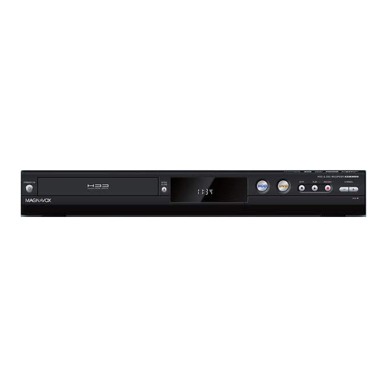
- Page 1 SERVICE MANUAL HDD & DVD PLAYER / RECORDER WITH DIGITAL TUNER H2080MW8...
-
Page 2: Table Of Contents
IMPORTANT SAFETY NOTICE Proper service and repair is important to the safe, reliable operation of all Funai Equipment. The service procedures recommended by Funai and described in this service manual are effective methods of performing service operations. Some of these service special tools should be used when and as recommended. -
Page 3: Specifications
SPECIFICATIONS ITEM General Internal 3.5 inch HDD 80 GB System DVD+RW/+R,DVD-RW/-R,DVD-video,CD-DA,Video CD,CD-RW/-R Power requirements 120V AC +/-10%,60HzV+/-5% TV format ATSC / NTSC-M TV standard Recording Recording format +VR (video recording) format Recordable discs DVD+ReWritable,DVD+Recordable DVD-ReWritable,DVD-Recordable (+VR mode only) Video recording format Sampling frequency 13.5MHz Compression format... -
Page 4: Laser Beam Safety Precautions
LASER BEAM SAFETY PRECAUTIONS This DVD player uses a pickup that emits a laser beam. Do not look directly at the laser beam coming from the pickup or allow it to strike against your skin. The laser beam is emitted from the location shown in the figure. When checking the laser diode, be sure to keep your eyes at least 30 cm away from the pickup lens when the diode is turned on. -
Page 5: Important Safety Precautions
IMPORTANT SAFETY PRECAUTIONS Product Safety Notice Also check areas surrounding repaired locations. J. Be careful that foreign objects (screws, solder Some electrical and mechanical parts have special droplets, etc.) do not remain inside the set. safety-related characteristics which are often not K. - Page 6 Safety Check after Servicing Examine the area surrounding the repaired location for damage or deterioration. Observe that screws, parts, and wires have been returned to their original positions. Afterwards, do the following tests and confirm the specified values to verify compliance with safety standards. 1.
-
Page 7: Standard Notes For Servicing
STANDARD NOTES FOR SERVICING Circuit Board Indications Pb (Lead) Free Solder 1. The output pin of the 3 pin Regulator ICs is When soldering, be sure to use the Pb free solder. indicated as shown. How to Remove / Install Flat Pack-IC Top View Bottom View 1. - Page 8 3. The flat pack-IC on the CBA is affixed with glue, so With Soldering Iron: be careful not to break or damage the foil of each 1. Using desoldering braid, remove the solder from pin or the solder lands under the IC when all pins of the flat pack-IC.
- Page 9 2. Installation With Iron Wire: 1. Using desoldering braid, remove the solder from 1. Using desoldering braid, remove the solder from all pins of the flat pack-IC. When you use solder the foil of each pin of the flat pack-IC on the CBA flux which is applied to all pins of the flat pack-IC, so you can install a replacement flat pack-IC more you can remove it easily.
- Page 10 Instructions for Handling Semi- conductors Electrostatic breakdown of the semi-conductors may occur due to a potential difference caused by electrostatic charge during unpacking or repair work. 1. Ground for Human Body Be sure to wear a grounding band (1 MΩ) that is properly grounded to remove any static electricity that may be charged on the body.
-
Page 11: Handling Precautions For Hdd
HANDLING PRECAUTIONS FOR HDD CAUTION: 4. OTHERS a. Be careful so as not to do the followings. 1. SHOCK Otherwise, HDD might be damaged. a. Exposing HDD to shock may be the biggest - DO NOT disassemble HDD. damaging factor. Please note that HDD is easily - When handling HDD, be sure to hold both sides damaged even if dropped from any height. -
Page 12: Cabinet Disassembly Instructions
CABINET DISASSEMBLY INSTRUCTIONS 1. Disassembly Flowchart REMOVAL This flowchart indicates the disassembly steps to gain REMOVE/*UNHOOK/ LOC. PART Fig. access to item(s) to be serviced. When reassembling, UNLOCK/RELEASE/ Note follow the steps in reverse order. Bend, route, and UNPLUG/DESOLDER dress the cables as they were originally. D5 4(S-6) Bracket [1] Top Cover... - Page 13 Reference Notes 1. Locking Tabs (L-1) ,(L-2) and (L-3) are fragile. Be careful not to break them. 1-1. Release five Locking Tabs (L-1). 1-2. Release three Locking Tabs (L-2) and remove the Front Assembly. (L-1) 1-3. Release two Locking Tabs (L-3). 2.
- Page 14 [8] ATA CBA [16] DTV Module [14] Power (S-12) CBA Unit Supply CBA CN3001 Module PCB [10] HDD Holder HDD Earth Plate (S-7) CN1001 (S-13) (S-13) (S-6) [9] HDD Bracket Fig. D5 [15] AV CBA (S-14) [17] Main PCB Holder [13] Motor DC Fan [12] Fan Cover Fan Earth...
- Page 15 4. How to Eject Manually Note: When rotating the gear, be careful not to damage the gear. 1. Remove the Top Cover. 2. Rotate the gear in the direction of the arrow manually as shown below until the tray descends. 3.
-
Page 16: How To Self-Check And Initialize The Hdd & Dvd Recorder
HOW TO SELF-CHECK AND INITIALIZE THE HDD & DVD RECORDER 1. Turn on the HDD & DVD. 2. To put the HDD & DVD into the HDD mode, press [HDD] on the remote control unit. 3. To put the HDD & DVD into the self-check mode, after pressing [V.SKIP] button, press the [0], [7], and [9] buttons on the remote control in that order within three seconds. - Page 17 Table 2: Indication of DVD self-check (*7) INDICATION DESCRIPTION Connection of DVD is normal. NOT FOUND DVD drive cannot be found. FFC cable (connecting to CN401) between the DVD drive and the DVD/HDD MAIN BOARD CABLE ERROR is not connected correctly. Table 3: Indication of HDD self-check (*8) INDICATION DESCRIPTION...
-
Page 18: Firmware Renewal Mode
FIRMWARE RENEWAL MODE 1. Turn the power on and remove the disc on the tray. 4. Select the firmware version pressing arrow buttons, then press [OK]. 2. To put the DVD recorder into version up mode, Fig. d appears on the screen and Fig. e appears press [V.SKIP], [6], [5], and [4] buttons on the on the VFD. -
Page 19: Function Indicator Symbols
FUNCTION INDICATOR SYMBOLS Note: If an error occurs, a message with the error number appears on the screen. Recording Error Error message You cannot record on this disc as Power Calibration Area is full. Error No. Error Message Solution Error Description Priority An error occurs during data reading. - Page 20 Error Message Solution Error Description Priority This program is not allowed to You cannot record cop-y During the CGMS picture input. (VR be recorded on this disc. prohibited programs. Format Disc) Release the disc protection This disc is protected and not setting in the Disc Setting Disc Protected Disc.
- Page 21 Error Message Solution Error Description Priority - Set the timer programming - Some portion has not been recorded correctly. because of program overlapping. - Set the timer programming - Recording did not start at the start time. before the start time. Error message is not displayed.
-
Page 22: Block Diagrams
BLOCK DIAGRAMS System Control Block Diagram 1-10-1 E2H00BLS... - Page 23 Digital Signal Process Block Diagram 1-10-2 E2H00BLD...
- Page 24 Video Block Diagram REAR FRONT 1-10-3 E2H00BLV...
- Page 25 Audio Block Diagram 1-10-4 E2H00BLA...
- Page 26 Power Supply Block Diagram 1-10-5 E2H00BLP...
- Page 27 DTV Module Block Diagram 1-10-6 E2H00BLDTV...
-
Page 28: Schematic Diagrams / Cba's And Test Points
SCHEMATIC DIAGRAMS / CBA’S AND TEST POINTS Standard Notes WARNING Many electrical and mechanical parts in this chassis have special characteristics. These characteristics often pass unnoticed and the protection afforded by them cannot necessarily be obtained by using replacement components rated for higher voltage, wattage, etc. - Page 29 LIST OF CAUTION, NOTES, AND SYMBOLS USED IN THE SCHEMATIC DIAGRAMS ON THE FOLLOWING PAGES: 1. CAUTION: FOR CONTINUED PROTECTION AGAINST FIRE HAZARD, REPLACE ONLY WITH THE SAME TYPE FUSE. ATTENTION: POUR UNE PROTECTION CONTINUE LES RISQES D'INCELE N'UTILISER QUE DES FUSIBLE DE MÊME TYPE. RISK OF FIRE-REPLACE FUSE AS MARKED.
- Page 30 AV 1/5 Schematic Diagram * NOTE These components (IC1502, C1509) can be used in any models. However, you cannot mix components under Group A with the ones under Group B. You can choose either Group. The difference between Group A and Group B is shown below. Group A Group B R3112N191A-TR-FA...
- Page 31 AV 2/5 Schematic Diagram 1-11-4 E2H00SCAV2...
- Page 32 AV 3/5 Schematic Diagram 1-11-5 E2H00SCAV3...
- Page 33 AV 4/5 Schematic Diagram E2H00SCAV4 1-11-6...
- Page 34 AV 5/5 Schematic Diagram FL1601 MATRIX CHART BS CS DR DTV BS CS 1-11-7 E2H00SCAV5...
- Page 35 Power Supply Schematic Diagram CAUTION ! For continued protection against fire hazard, CAUTION ! replace only with the same type fuse. Fixed voltage (or Auto voltage selectable) power supply circuit is used in this unit. NOTE: ATTENTION : Pour une protection continue les risqes The voltage for parts in hot circuit is measured using If Main Fuse (F2001) is blown , check to see that all components in the power supply d'Incele n'utiliser que des fusible de même type.
- Page 36 Front SW & Power SW Schematic Diagram ATA Schematic Diagram E2H00SCFSW E2H00SCATA 1-11-9...
- Page 37 DVD/HDD Main 1/5 Schematic Diagram 1 NOTE: The order of pins shown in this diagram is different from that of actual IC101. IC101 is divided into five and shown as IC101 (1/5) ~ IC101 (5/5) in this DVD/HDD Main Schematic Diagram Section. 1-11-10 E2H00SCD1...
- Page 38 DVD/HDD Main 2/5 Schematic Diagram 1 NOTE: The order of pins shown in this diagram is different from that of actual IC101. IC101 is divided into five and shown as IC101 (1/5) ~ IC101 (5/5) in this DVD/HDD Main Schematic Diagram Section. 1-11-11 E2H00SCD2...
- Page 39 DVD/HDD Main 3/5 Schematic Diagram 1 NOTE: The order of pins shown in this diagram is different from that of actual IC101. IC101 is divided into five and shown as IC101 (1/5) ~ IC101 (5/5) in this DVD/HDD Main Schematic Diagram Section. E2H00SCD3 1-11-12...
- Page 40 DVD/HDD Main 4/5 Schematic Diagram 1 NOTE: The order of pins shown in this diagram is different from that of actual IC101. IC101 is divided into five and shown as IC101 (1/5) ~ IC101 (5/5) in this DVD/HDD Main Schematic Diagram Section. 1-11-13 E2H00SCD4...
- Page 41 DVD/HDD Main 5/5 Schematic Diagram 1 NOTE: The order of pins shown in this diagram is different from that of actual IC101. IC101 is divided into five and shown as IC101 (1/5) ~ IC101 (5/5) in this DVD/HDD Main Schematic Diagram Section. E2H00SCD5 1-11-14...
- Page 42 DTV Module 1/2 Schematic Diagram 1-11-15 E2H00SCDTV1...
- Page 43 DTV Module 2/2 Schematic Diagram E2H00SCDTV2 1-11-16...
- Page 44 AV CBA Top View BE2H40F01011A 1-11-17...
- Page 45 AV CBA Bottom View PIN 3 OF CN1051 PIN 3 OF CN1101 PIN 5 OF CN1101 PIN 7 OF CN1101 C1418 PLUS LEAD PIN 9 OF CN1101 PIN 17 OF CN1101 B2H40F01011A 1-11-18...
- Page 46 Power Supply CBA Top View CAUTION ! Because a hot chassis ground is present in the power CAUTION ! supply circut, an isolation transformer must be used. Fixed voltage (or Auto voltage selectable) power supply circuit is used in this unit. For continued protection against fire hazard, If Main Fuse (F2001) is blown , check to see that all components in the power supply Also, in order to have the ability to increase the input...
- Page 47 Power Supply CBA Bottom View CAUTION ! Because a hot chassis ground is present in the power CAUTION ! supply circut, an isolation transformer must be used. Fixed voltage (or Auto voltage selectable) power supply circuit is used in this unit. For continued protection against fire hazard, If Main Fuse (F2001) is blown , check to see that all components in the power supply Also, in order to have the ability to increase the input...
- Page 48 Power SW CBA Power SW CBA Front SW CBA Top View Bottom View Top View BE2H40F01011C Front SW CBA Bottom View ATA CBA Top View ATA CBA Bottom View BE2H40F01011B BE4340F01032 1-11-21...
-
Page 49: Waveforms
WAVEFORMS Pin 7 of CN1101 Pin 5 of CN1101 VIDEO-Y 0.2V 20µsec VIDEO-Cr 0.2V 20µsec Pin 9 of CN1101 Pin 17 of CN1101 VIDEO-C 0.2V 20µsec AUDIO(L)-OUT 0.5ms C1418 PLUS LEAD Pin 3 of CN1051 VIDEO-CVBS 0.5V 20µsec SPDIF 0.1µsec Pin 3 of CN1101 NOTE: Input: COLOR BAR SIGNAL... -
Page 50: Wiring Diagram
WIRING DIAGRAM Wiring 1/2 Diagram 1-13-1 E2H00WI1... - Page 51 Wiring 2/2 Diagram 1-13-2 E2H00WI2...
-
Page 52: System Control Timing Charts
SYSTEM CONTROL TIMING CHARTS [ Tray Open ] Push Close Power on button is pressed. Tray insertion INNER-SW open? Tray insertion INNER-SW open? Tray ejection To disc distinction [ Tray Open ] button is pressed. INNER-SW open? SLED moves Tray ejection 1-14-1 R4NTI... - Page 53 Parameter V*: Voltage T*: Event timer V0: 2.40 V T1: 0.050 s V1: 4.25 V T2: 2.000 s V2: 2.00 V T3: 0.008 s V3: 2.36 V T4: 0.006 s V4: 4.26 V T5: 0.066 s T6: 1.500 s T7: 0.800 s T8: 0.005 s Tray open Tray ejection direction...
- Page 54 Push close Threshold level 0.08 V 0.02 s Push Close detection 1-14-3 R4NTI...
-
Page 55: Ic Pin Function Descriptions
IC PIN FUNCTION DESCRIPTIONS IC1501 (SUB MICROCONTROLLER) Signal Function Name Signal Function Power Voltage Down Name IN P-DOWN Detector Signal IN KEY-1 Key Data Input 1 31 OUT FL-SEL FL Select (Low Level) IN KEY-2 Key Data Input 2 Not Used Power Supply Failure IN SAFETY1 Detection 1... - Page 56 Signal Function Name Not Used Not Used Power Supply Failure SAFETY2 Detection 2 IC1602 (VFD DRIVER Signal Function Name IN CLK Serial Clock IN STB Serial Interface Strobe Not Used Not Used Power Supply Segment Output Pull Down Level 16 OUT i Segment Output Grid Output Power Supply...
-
Page 57: Lead Identifications
LEAD IDENTIFICATIONS KTC3203-Y-AT/P KRC103M-AT/P 2SK3561(Q) TLV1117I TO-220 KTC3205-Y-AT/P KTA1267-(GR,Y)-AT/P KTC3199-(BL,GR,Y)-AT/P ADJ/GND INPUT G D S OUTPUT E C B E C B UTC4580E MM1697AJBE AN5832SA-E1V PQ070XF01SZH KTB1151-Y-U/P 1 2 3 4 E C B MN101C77AFP1 MM1637XVBE CD4052BNSR SC16313G KTC2026-Y/P BU4219G-TR KIA431-AT/P R3112N191A-TR-FA PS2561A-1(W) -
Page 58: Exploded Views
EXPLODED VIEWS Cabinet ATA CBA 2L010 2B26 2L071 See Electrical Parts List for parts with this mark. 2L040 2L040 2L010 2L030 2B49 DVD MECHANISM & DVD/HDD MAIN CBA ASSEMBLY 2L050 2L070 2B10 2L070 2B10 2L044 2L050 2B15 2L040 2B20 2L040 2L010 POWER SUPPLY CBA AC2001... - Page 59 Packing Lower Side Upper Side Unit Some Ref. Numbers are not in sequence. 1-17-2 E2H00PEX...
-
Page 60: Mechanical Parts List
MECHANICAL PARTS LIST PRODUCT SAFETY NOTE: Products marked with a Ref. No. Description Part No. # have special characteristics important to safety. QUICK GUIDE E2H00UD 1VMN23646 Before replacing any of these components, read carefully the product safety notice in this service manual. -
Page 61: Electrical Parts List
ELECTRICAL PARTS LIST PRODUCT SAFETY NOTE: Products marked with a Ref. No. Description Part No. # have special characteristics important to safety. C1029 ELECTROLYTIC CAP . 1000µF/6.3V M CE0KMASDL102 Before replacing any of these components, read C1069 CHIP CERAMIC CAP .(1608) F Z 0.1µF/50V CHD1JZ30F104 carefully the product safety notice in this service C1101... - Page 62 Ref. No. Description Part No. Ref. No. Description Part No. C1502 CHIP CERAMIC CAP .(1608) F Z 0.1µF/50V CHD1JZ30F104 C1757 ELECTROLYTIC CAP . 100µF/6.3V M CE0KMASDL101 C1503 CHIP CERAMIC CAP .(1608) F Z 0.1µF/50V CHD1JZ30F104 C1759 ELECTROLYTIC CAP . 100µF/6.3V M CE0KMASDL101 C1506 CHIP CERAMIC CAP .(1608) CH J 22pF/50V...
- Page 63 Ref. No. Description Part No. Ref. No. Description Part No. D1720 ZENER DIODE MTZJT-7733B QDTB00MTZJ33 Q1304 TRANSISTOR KTC3199-GR-AT/P NQS4KTC3199P D1753 SWITCHING DIODE 1SS133(T-77) QDTZ001SS133 Q1501 TRANSISTOR KTA1267-GR-AT/P NQS1KTA1267P Q1502 TRANSISTOR KTC3199-GR-AT/P NQS4KTC3199P Q1505 NPN TRANSISTOR KRC103M-AT/P NQSZKRC103MP IC1001 IC REGULATOR TLV1117I TO-220 NSZBA0STY245 Q1506 NPN TRANSISTOR KRC103M-AT/P...
- Page 64 Ref. No. Description Part No. Ref. No. Description Part No. CHIP RES. 1/10W J 18k Ω CHIP RES. 1/10W J 100 Ω R1128 RRXAJR5Z0183 R1513 RRXAJR5Z0101 CHIP RES. 1/10W J 300 Ω CHIP RES. 1/10W J 47k Ω R1139 RRXAJR5Z0301 R1514 RRXAJR5Z0473 CHIP RES.
- Page 65 Ref. No. Description Part No. Ref. No. Description Part No. CHIP RES. 1/10W J 180k Ω CHIP RES. 1/10W J 1k Ω R1701 RRXAJR5Z0184 R3003 RRXAJR5Z0102 CHIP RES. 1/10W J 3.3k Ω CHIP RES. 1/10W J 2.2k Ω R1704 RRXAJR5Z0332 R3004 RRXAJR5Z0222 CHIP RES.
- Page 66 Ref. No. Description Part No. Ref. No. Description Part No. CONNECTOR R2120 PCB JUMPER D0.6-P5.0 JW5.0T CHIP RES. 1/10W J 1.5k Ω R2212 RRXAJR5Z0152 CN2001 WIRE ASSEMBLY FFC PW-AV 34PIN WX1E2H40-003 WX1E2H40-003 CHIP RES. 1/10W J 15k Ω R2213 RRXAJR5Z0153 DIODES METAL OXIDE FILM RES.
- Page 67 Misuse of any trademarks or any other content in this manual is strictly prohibited. Funai shall aggressively enforce its intellectual property rights to the fullest extent of the law. H2080MW8 E2H00UD 2007-07-25...
Need help?
Do you have a question about the H2080MW8 and is the answer not in the manual?
Questions and answers