Denon D-T1 Service Manual
Cd receiver system
Hide thumbs
Also See for D-T1:
- Owner's manual (73 pages) ,
- Quick start manual (13 pages) ,
- Quick start manual
Advertisement
Quick Links
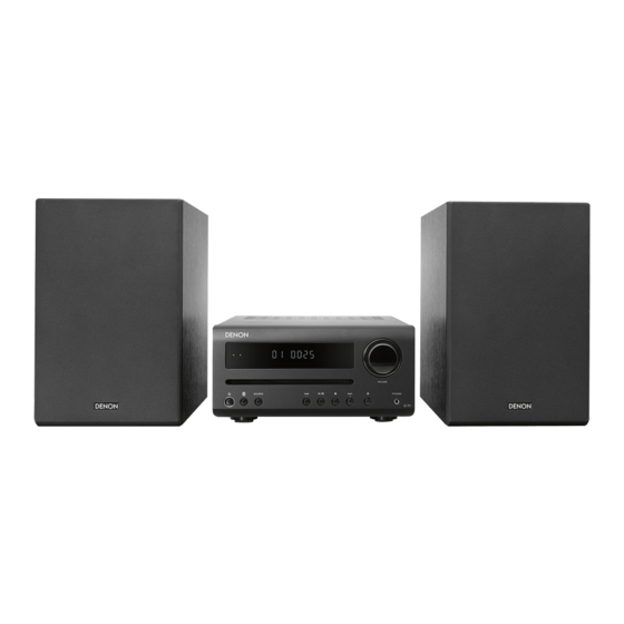
CD RECEIVER SYSTEM
D-T1
• For purposes of improvement, specifications and design are subject to change without notice.
• Please use this service manual when referring to the operating instructions without fail.
• Some illustrations used in this service manual are slightly different from the actual product.
Service Manual
Click here!
On-line service parts list
http://dmedia.dmglobal.com/Document/DocumentDetails/25094
ONLINE PARTS LIST
(P5)
WEBマニュアル
NA:
http://manuals.denon.com/DT1/NA/EN/index.php
EU:
http://manuals.denon.com/DT1/EU/EN/index.php
AP:
http://manuals.denon.com/DT1/AP/ZH/index.php
JP:
http://manuals.denon.com/DT1/JP/JA/index.php
Upload is planned for the time of a future press release.
BEFORE SERVICING THIS UNIT
ELECTRICAL
MECHANICAL
REPAIR INFORMATION
UPDATING
Confidential
Ver. 1
Advertisement

Related Manuals for Denon D-T1


Summary of Contents for Denon D-T1
- Page 1 Service Manual Ver. 1 CD RECEIVER SYSTEM D-T1 Click here! On-line service parts list http://dmedia.dmglobal.com/Document/DocumentDetails/25094 ONLINE PARTS LIST (P5) WEBマニュアル http://manuals.denon.com/DT1/NA/EN/index.php http://manuals.denon.com/DT1/EU/EN/index.php http://manuals.denon.com/DT1/AP/ZH/index.php http://manuals.denon.com/DT1/JP/JA/index.php Upload is planned for the time of a future press release. BEFORE SERVICING THIS UNIT ELECTRICAL...
- Page 2 BEFORE SERVICING THIS UNIT SAFETY PRECAUTIONS NOTE FOR SCHEMATIC DIAGRAM HANDLING THE SEMICONDUCTOR AND OPTICS WARNING AND LASER SAFETY INSTRUCTIONS ONLINE PARTS LIST Accessing the Parts List Searching Part Numbers or Ref. Numbers NOTE FOR PARTS LIST SERIAL NUMBER Serial Number Organization SKU Code of this Unit POST-SERVICE PRECAUTIONS Initializing this Unit...
- Page 3 SAFETY PRECAUTIONS The following items should be checked for continued protection of the customer and the service technician. Leakage current check Before returning the set to the customer, be sure to carry out either (1) a leakage current check or (2) a line to chassis resistance check. If the leakage current exceeds 0.5 milliamps, or if the resistance from chas- sis to either side of the power cord is less than 460 kohms, the set is defective.
- Page 4 NOTE FOR SCHEMATIC DIAGRAM WARNING AND LASER SAFETY INSTRUCTIONS WARNING: WARNING WAARSCHUWING Parts indicated by the z mark have critical characteristics. Use ONLY replacement parts recommended Alle IC’s en vele andere halfgeleiders zijn gevoelig All ICs and many other semi-conductors are voor elektrostatische ontladingen (ESD).
- Page 5 ONLINE PARTS LIST Accessing the Parts List Searching Part Numbers or Ref. Numbers (1) Access from the Service Manual You can search a Parts List for part numbers or Ref. numbers. ・ Click the URL link on the cover of the service manual. (1) Enter the part number or Ref.
- Page 6 SERIAL NUMBER Serial Number Organization The 14-digit serial number that contains the code of the manufacturing plant and the manufacturing date. 14 digits Factory Manufactured Cumulative Year, month code code serial number The last Month 2digit of year (01 ~ 12) SKU Code of this Unit Product SKU SKU Code...
- Page 7 POST-SERVICE PRECAUTIONS Initializing this Unit Make sure to initialize this unit after replacing the microcomputer or any peripheral equipment, or the PCB. 1. While the power is On, hold down buttons "SOURCE" and "EJECT" for at least 5 seconds. 2. "RESET" is displayed for 3 seconds. 3.
- Page 8 ELECTRICAL SCHEMATIC DIAGRAMS SCH01 MAIN1 DC POWER SCH02 MAIN2 DC MOS SW SCH03 MAIN3 SP8104 & CD SCH04 MAIN4 SDRAM & TUNER SCH05 MAIN5 MCU&RTC & Connector SCH06 MAIN6 BT & ADC SCH07 MAIN7 AMP & EAR SCH08 VFD SCH09 Power PRINTED CIRCUIT BOARDS DISPLAY, MAIN, POWER BLOCK DIAGRAM...
- Page 9 SCHEMATIC DIAGRAMS SCH01 MAIN1 DC POWER VOUT=0.6*(200K+43.2K)/43.2K=3.38v STB_5V STB_3V3 1uH/2.7A 100K POWER_14V 200K/1% MP1605 10uF/10V/X5R POWER_FRQ1 330pF/50V/X7R 0.1uF/50V/X7R POWER_FRQ2 43.2K/1% For select different frq of power SW 6PIN/2.0mm 100pF/50V/NP0 From Power Board 100pF/50V/NP0 0.8*(8.2+15)/15=1.23V VCC12 SYS_3V3 SMG2036ADJ STB_5V POWER_14V VOUT Vout=(120K/22k+1)*0.8=5.16V 8.2K/1% 0.01uF/50V/X7R...
- Page 10 SCH02 MAIN2 DC MOS SW LT1527SL STB_5V SYS_5V POWER_14V AMP_14V STB_3V3 SYS_3V3 680K 0.1uF/50V/X7R 510KΩ/1% P_AP2305 P_AP2305 470K 470K 4.7K CE273 220uF35V PCON 4.7K NPN_3DG3904M TP52 PCON 4.7K NPN_3DG3904M 4.7K 0.1uF/16V/X7R POWER_EN NPN_3DG3904M 0.1uF/16V/X7R 0.1uF/16V/X7R POWER CONTROL AMP_14V POWER CONTROL 5V POWER CONTROL SYS_3V3 FM3V3 STB_BT_3V3...
- Page 11 SCH03 MAIN3 SP8104 & CD PUHRF USB_DP USB_DM R41 4.7K RF3.3V SYS_5V I2C_SDA R42 500Ω/100mA AMP_SDA SF_CS 0.1uF/16V/X7R AMP_SDA SF_DO 4.7K NC/4PIN/2.0mm R44 500Ω/100mA TUNER_SDA HOLD# SF_CK TUNER_SDA SF_DI VCC1.2 VCC1.2 EN25QH16B-104HIP2A 16Mb NOR FLASH SOP8 MPEG_TX MPEG_RX NC/1uF/10V/X5R R47 4.7K 10uF/10V/X5R NC/4PIN/2.0mm I2C_SCL...
- Page 12 SCH04 MAIN4 SDRAM & TUNER SDRAM Go to display board -24pin FFC XP10 Go to display board -5pin cable 220Ω VFD_14V 220Ω -24V -24V VFD_CS FB32 600Ω/0.3A EAR_OUT_L VFD_CS POWER_KEY FB12 600/200mA EAR_OUT_L FB33 600Ω/0.3A EAR_OUT_R POWER_KEY VFD_CLK FB11 600/200mA EAR_OUT_R FB34 600Ω/0.3A...
- Page 13 SCH05 MAIN5 MCU&RTC & Connector PCON PCON BT_POWER_SW TP45 TP46 STB_MCU_3V3 STB_MCU_3V3 STB_MCU_3V3 STB3.3V STB3V3 STB_MCU_3V3 R129 STB_MCU_3V3 R128 R130 PC13 SWDIO POWER_EN PC14/OSC32_IN PA13 R131 R132 R133 R134 R304 Tuner_Power_SW PC15/OSC32_OUT PA12 BT_RESET PF0/OSC_IN PA11 AMP_FAULT R135 R137 R311 R136 MCU_RST PF1/OSC_OUT...
- Page 14 SCH06 MAIN6 BT & ADC ADC_BCLK R171 6,11 ADC_MCLK ADC_BCLK 30K/1% ADC_LRCK ADC_MCLK 6,11 6,11 ADC_DATA ADC_LRCK ADC_DATA cis updata already C150 4.7uF R172 R173 15K/1% C151 4.7uF BT_R C152 4.7uF R175 R174 15K/1% 4052_SW1 F4558M 4052_SW2 4052_SW1 R177 R178 R176 TUNER_SCL 4052_SW2...
- Page 15 SCH07 MAIN7 AMP & EAR COMPATIBLE +3.3VDD FB46 500Ω/200mA AMP_14V R239 220K R378 NC/22 AMP_ADC_3V3 +3.3VD C313 NC/0.1uF/50V/X7R R240 FB21 500Ω/200mA +3.3VD FB22 300Ω/3A C188 220K 10uF/25V CE14 FB23 500Ω/200mA Horn carrier WP4-1-02Z1 50V R241 220K CE13 220uF50V 100uF/16V C301 VDD_DIG GND_SUB R377...
- Page 16 SCH08 VFD +13V VFD1 FB10 1.8uH/25mA +13V FB11 1.8uH/25mA -24V -24V +5VA VFD_CS 1.8uH/25mA +12VA POWER_KEY VFD_CLK 2.2Ω ADC_KEY2 NPN_3DG3904M VFD_DATA NPN_3DG3904M ADC_KEY1 0.1uF/50V/X7R 3.3uF/50V 330/1% VOL- NPN_3DG3904M LED_GRE 8.2K 4.7K VOL+ LED_RED PNP_3CG3906M 3.3uF/50V BT_LED NPN_3DG3904M STB_BT_5V -24V 20PIN/1.0mm -24V 3300pF/50V/X7R SEG8...
- Page 17 SCH09 Power C508 0.0022uF(222)400V D555 D556 R5021 R5022 R5023 R5024 FR207/2A/1000V NC/150K NC/150K FR207/2A/1000V R503 NC/270K NC/150K CY503 1000pF/250VAC C570 CE501 CE502 R508 22nF ZD503 33uF/400V 33uF/400V P6KE200A 22Ω D554 D553 FR207/2A/1000V FR207/2A/1000V R501 T501 R504 R551 100 36-TRF356-SX0-E R552 NC/100 C551 1000pF/630V D505 D551...
- Page 18 PRINTED CIRCUIT BOARDS DISPLAY, MAIN, POWER Lead-free Solder When soldering, use the Lead-free Solder (Sn-Ag-Cu). DISPLAY(A SIDE) DISPLAY(B SIDE) MAIN(A SIDE) MAIN(B SIDE) POWER (A SIDE) POWER (B SIDE) XP16 C137 R162 R143 TP47 LIF551 R146 ANT1 R145 C156 FB10 R360 R193 C157...
- Page 19 BLOCK DIAGRAM flash SDRAM 27MHz 16Mbit 64Mbit LOADER (VSH-M33DS- Motor Driver VFD Driver VFD Display D1206V(KT) AM5890 CS6312 8 fonts S76RFS7GP) 6Ω TW 6Ω WF PWM1 SPDIF 15W 10% Optical in Amplifier STA339BWS PWM2 6Ω TW SUNPLUS KST- 6Ω WF MW104MV 15W 10% 1-R75B...
- Page 20 POWER DIAGRAM -24V 15mA VFD + Audio_SW 500mA STB_5V Moter Driver 330mA 1000mA Internal DC-DC AM5890S TPS54335 15V/2.3A 530mA SYS_5V AP2305 1.9A LT527SL AMP_15V 20mA AC 110- AP2305 BT_LED 230V VFD_14V INPUT R_G_O_LED 25mA 20mA 140mA SGM2036 25mA VCC_1.2V for OP_BT SGM2202 SP8104...
- Page 21 WIRING DIAGRAM...
- Page 22 SEMICONDUCTORS Only major semiconductors are shown, general semiconductors etc. are omitted to list. The semiconductor which described a detailed drawing in a schematic diagram are omitted to list. 1. IC's ST32F030R8 (U10 : MCU) Pin function Pin functions Pin name (function after struc- Notes reset)
- Page 23 Pin functions Pin name (function after struc- Notes reset) type ture Alternate functions Additional functions PA10 USART1_RX, TIM1_CH3, TIM17_BKIN I2C1_SDA(2)(5) PA11 USART1_CTS, TIM1_CH4, EVENTOUT, I2C2_SCL(5) PA12 USART1_RTS, TIM1_ETR, EVENTOUT, I2C2_SDA(5) PA13 (SWDIO) IR_OUT, SWDIO 47(4) PF6 I2C1_SCL(2), I2C2_SCL(3) 47(5) VSS Ground 48(4) PF7 I2C1_SDA(2), I2C2_SDA(3)
- Page 24 SP8104-WWX(Suplus) (U5 : DSP) Symbol I/O Description Symbol I/O Description M_D9 I/O SDRAM data bus bit 9 AD_AVDD P 3.3V power for Servo ADC External AGC capacitor connected to M_D8 I/O SDRAM data bus bit 8 AGCCAP ground. (0.1u) SDRAM data input/output mask for M_DQM1 RFIS Single-ended RF equalizer input.
- Page 25 SGM2202ADJ (U3,U27,U28) SGM2036 (U2 : SGM2036) SGM2202-ADJ VOUT BP/FB Pin function SOT-23-6 Pin function NAME FUNCTION UTDFN-1 SOT-23-5/ × 1-4L SC70-5 NAME FUNCTION SOT-23-6 Regulator Output. Regulator Input. Up to 36V input voltage. At least 1 μ F supply bypass capacitor is recommended. Ground.
- Page 26 AM5890S_V1.5TS (U6 : Driver) AK5358BET (U16 : ADC) MUTE BIAS VINTK TRB_2 RESET VINLD VCTL VCCD VCC2 VOLD- VOLD+ VOTK- VOTK+ AINR CKS0 AINL CKS2 PGND Vcc2 Voltage CKS1 Detection MUTE VCOM Spindle Actuator Top View Driver(6x) Driver(4X) VSS1 SCLK Thermal Shut down MCLK...
- Page 27 STA339BWS (U19 : STA339BW) SGM4917 (U24 : HP_AMP) (TOP VIEW) GND_SUB VDD_DIG GND_DIG TEST_MODE OUTL VCC_REG INT_LINE OUT2B RESET GND2 VCC2 LRCKI PGND OUTR OUT2A BICKI OUT1B VCC1 GND_PLL GND1 FILTER_PLL OUT1A VDD_PLL EP, exposed pad GND_REG PWRDN TQFN-3×3-16L (device ground) GND_DIG Pin function CONFIG...
- Page 28 ANODE CONNECTION 2. FL DISPLAY FV935 (VFD1) col 2G, 4G, 6G 1G-8G PIN CONNECTION NOTE 1) F1, F2 ----Filament 2) NP ------No pin 3) NC ------No connection (NC pin should be electrically open on the PC board.) 4) DL ------Datum Line 5) 1G-8G --Grid 6) Solder composition is Sn-3Ag-0.5Cu.
- Page 29 3. Remote Code Table KEY CODE (Kaseikyo Code) D-T1:RC-1229 Maker Code (C Byte 1 Byte 2 DENON (3254H) 00101010 01001100 KEY No. Name Genre 1(D Genre 2(D DATA Code (D Parity (D Byte 3 Byte 4 Byte 5 Byte 6...
- Page 30 MECHANICAL DISASSEMBLY Flowchart 1. FRONT ASSY 2. CD MECHA ASSY 3. MAIN PCB 4. POWER PCB EXPLODED VIEW PACKAGING VIEW...
- Page 31 DISASSEMBLY Flowchart • Remove each part following the flow below. • Reassemble the removed parts in the reverse order. • Read "SAFETY PRECAUTIONS" before reassembling the removed parts. • If wire bundles are removed or moved during adjustment or part replacement, reshape the wires after completing the work. Failure to shape the wires correctly may cause problems such as noise. • See "EXPLODED VIEW" TOP COVER FRONT ASSY MAIN PCB DISASSEMBLY DISASSEMBLY 1. FRONT ASSY 3. MAIN PCB and "EXPLODED VIEW" and "EXPLODED VIEW" FRONT PCB MAIN PCB Ref. No. of EXPLODED VIEW : 11 Ref. No. of EXPLODED VIEW : 26 Bluetooth antenna Ref. No. of EXPLODED VIEW : 5 CD MECHA ASSY POWER PCB DISASSEMBLY DISASSEMBLY 2. CD MECHA ASSY 4. POWER PCB and "EXPLODED VIEW" and "EXPLODED VIEW" Suction Loader Main board support Ref. No. of EXPLODED VIEW : 13 Ref. No. of EXPLODED VIEW : 24...
- Page 32 • For the shooting direction of each photos used in this manual, see the photo below. • A, B, C and D in the photo below indicate the shooting directions of photos. Proceeding : TOP COVER → FRONT ASSY • The photographs with no shooting direction indicated were taken from the top of the unit. (1) Remove the hook. • Photos of D-T1 E2 are used in this manual. The viewpoint of each photograph (Shooting direction : X) [View from the top] ↓Shooting direction: B↓ Hook x4 View from the bottom (1) Remove the connector. Remove the FFC. Remove the wire from the antenna, along with the glue. Hook ↑Shooting direction: A↑...
- Page 33 2. CD MECHA ASSY 3. MAIN PCB Proceeding : TOP COVER → FRONT ASSY → CD MECHA ASSY Proceeding : TOP COVER → MAIN PCB (1) Remove the screws. (1) Remove the screws. Remove the connector. Remove the FFC. Remove the wire from the antenna, along with the glue. Hook Glue Glue ↑Shooting direction: A↑ ↑Shooting direction: A↑...
- Page 34 4. POWER PCB Proceeding : TOP COVER → MAIN PCB → POWER PCB (1) R emove the screws. Remove the Main board support. Remove the screws. Remove the connector. Main board support CN501...
- Page 35 EXPLODED VIEW http://dmedia.dmglobal.com/Document/DocumentDetails/25094 Parts List : WARNING: Parts marked with this symbol z have critical characteristics. Use ONLY replacement parts recommended by the manufacturer.
- Page 36 PACKAGING VIEW http://dmedia.dmglobal.com/Document/DocumentDetails/25094 Parts List : E2 Version ZIPPERBAG E3 Version ZIPPERBAG 12-1 SAFETY INST. (ALL) 12-1 SAFETY INST. (ALL) 12-2 Cautions on Using Batteries (E2 Only) 12-3 Notes on RADIO. (ALL) 12-3 Notes on RADIO. (ALL) 12-4 WARRANTY USA & CANADA (E3 Only) 12-5 FM Antenna 12-5 FM Antenna JP Version ZIPPERBAG...
- Page 37 REPAIR INFORMATION TROUBLE SHOOTING 1. The unit will not power on (protection is activated) 2. The unit will not power on (other cause) 3. VFD is not lit 4. The disc is not ejected 5. The disk is not loaded, or is not played. 6.
- Page 38 TROUBLE SHOOTING 1. The unit will not power on (protection is activated) Checking the "2. The unit will not power on (other The Power LED (red) is blinking. cause)". D-AMP protection is activated. Check for abnormalities in the power supply. 44pin (AMP_FAULT) for [U10 : STM32F030] is SYS_3V3, SYS_5V, STB_3V3 "Lo"...
- Page 39 2. The unit will not power on (other cause) Check the state / soldering for the following Check of SYS_3.3V. Check the state / soldering for the following Check of POWER 14V. parts. MAIN PCB parts. SMPS PCB MAIN PCB Voltage is supplied as normal to [Q3 : Drain].
- Page 40 3. VFD is not lit 4. The disc is not ejected Check the power supply of the VFD driver Check the state / soldering for the following When the " 5 " button is pressed, there is no Replace the mechanical. (VFD14V) parts.
- Page 41 5. The disk is not loaded, or is not played. 6. No audio output. 6.1. No sound is output from any inputs Check the state / soldering for the following Check the operation of the " 1 / 3 " button. parts.
- Page 42 6.3. No sound is output from inputs except DIGITAL IN 6.4. Abnormality in specific source 6.4.1. Abnormality in TUNER No sound is output from the TUNER, ANALOG IN No issues in circuits after Function SEL. and BLUETOOTH inputs Go to "6.4.
- Page 43 6.4.2. Abnormality in BLUETOOTH 6.4.3. Abnormality in ANALOG IN Check the Audio Line of ANALOG IN. No sound is output from the BLUETOOTH input Go to "6.4.3. Abnormality in ANALOG IN" MAIN PCB source [P1 : 1, 3pin] → [U17 : 4, 11pin] Check the Control Port of BT Module.
- Page 44 7. No audio from headphones. Check the Detection circuit of Headphone. Check the status of the headphone detection MAIN PCB circuit as follows [U10 : 40pin] Check the circuit from MAIN PCB [U10 : 40pin] to [U10: 40pin] changes from Lo to Hi when head- DISPLAY PCB [XP3 : 5, 8pin].
- Page 45 SPECIAL MODE Special mode setting button b No. 1 : With the power on, press the "CLEAR" → "LEFT" → "STOP" buttons on the remote control. b No. 2, 3 : While the power is on, hold down buttons "A" and "B" for at least 5 seconds . Mode Button A Button B...
- Page 46 1. Version Display Mode 3. Initialization Mode 1.1. Actions Make sure to initialize this unit after replacing the microcomputer or any peripheral equipment, or the PCB. Version information is displayed when the device is started in this mode. 3.1. Operations 1.2.
- Page 47 UPDATING PROCEDURE AFTER REPLACING THE PCB. PROCEDURE AFTER REPLACING THE U-COM, ETC. FIRMWARE UPDATE PROCEDURE 1. Items necessary for update 2. Updating via Disc 3. Updating via DSP (U4) 4. MCU Updates (U10)
- Page 48 PROCEDURE AFTER REPLACING THE PCB. PROCEDURE AFTER REPLACING THE U-COM, ETC. The firmware of U4 (EN25QH16B-104HIP2A) in the MAIN PCB differs depending on the region. The procedure after replacing the u-COM (microprocessor), flash ROM, etc. is as follows. Be sure to follow the instructions in "FIRMWARE UPDATE PROCEDURE"...
- Page 49 FIRMWARE UPDATE PROCEDURE 1. Items necessary for update Items necessary for update are as follows. Offered / not Offered Update Type Needed Part for Update Requirement Standard Service Equipment Purchase from D&M Article code Download from SDI Not offered by D&M File name for MCU : DM_MICRO_MCU.bin Via Disc...
- Page 50 2. Updating via Disc 4. MCU Updates (U10) The latest firmware can be written to a disc for update. 4.1. Preparation • Use the Disc created in "2.2. How to create a disc". 2.1. Support Disc Preparation 4.2. Operations • Provide a writable CD-R/RW disc. (1) Press the power button to turn on the power.
- Page 51 Copyright © 2018 D&M Holdings Inc. All Rights Reserved.
Need help?
Do you have a question about the D-T1 and is the answer not in the manual?
Questions and answers