
Subscribe to Our Youtube Channel
Related Manuals for Datron PRC1099A


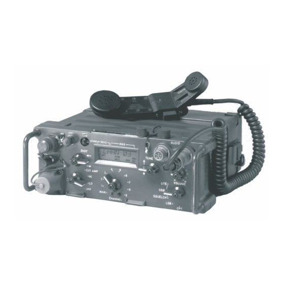
Summary of Contents for Datron PRC1099A
- Page 1 PRC1099A HF Transceiver Technical Manual Manual Part No. PRC1099A-MS Release Date: February 2017 Revision: S...
- Page 2 Datron World Communications Inc. 995 Joshua Way, Suite A Vista, CA 92081, U.S.A. Phone: (760) 597-1500 Fax: (760) 597-1510 E-Mail: customerservice@dtwc.com www.dtwc.com...
- Page 3 Revised to describe new Synthesizer board. Chapter 3 Chapter 4 5/10 Battery pack, weight, duty cycle, audio specs. Add internal option PRC1099A-IP. 1-3, 6-19 Remove reference to internal option (1099AME). Chapter 6 Update boards, schematics, part lists. Chapters 3, 4, 6...
- Page 5 It should not be construed as a commitment by In such an event, Datron will provide the user with written notice Datron. Datron assumes no responsibility or liability for any of such a “failure-to-comply” and the user will have 10 days to errors or inaccuracies that may appear in this book.
- Page 6 Buyer’s sole remedies and the entire liability of Datron are set lightning, static discharge, voltage transients, or forth above. In no event will Datron be liable to Buyer or any application of incorrect supply voltages. other person for any damages, including any incidental or...
- Page 7 AC plug. DO NOT attempt to disable the ground attention. terminal by using 2-wire adapters of any type. Any Use only genuine Datron factory parts for full performance and disconnection of the equipment ground causes a potential safety of this product.
-
Page 9: Table Of Contents
1.1 The PRC1099A ........ - Page 10 6.1 Circuit Description ......... 6-1 Figure 6-1 Power Amplifier Board Block Diagram ......6-1 viii PRC1099A-MS...
- Page 11 Figure 8-8 Synthesizer Board Schematic Diagram 6 of 6 (994073 Rev. D)..8-17 Table 8-3 Synthesizer Board Parts List (009-00606 Rev. P) ....8-19 PRC1099A-MS...
- Page 12 Junction Board Schematic Diagram (994164 Rev. F) ... .11-5 Table 11-3 Junction Board Parts List (009-00901 Rev. W) ....11-7 PRC1099A-MS...
- Page 13 ALE Board Parts List (010-00200 Rev. V) ....13-11 13.2 Internet Protocol Interface (PRC1099A-IP)....13-14 Chapter 14: Maintenance 14.1 Test Equipment .
- Page 14 PA Board Adjustments ........14-27 Figure 14-10 PA Board Signal Connections and Adjustment Points ...14-27 PRC1099A-MS...
-
Page 15: Chapter 1: Introduction
Chapter 1: Introduction The PRC1099A The PRC1099A is an HF/SSB tactical manpack transceiver designed for demanding high-visibility battlefield applications. It is rugged, lightweight, easy to use, and configurable with numerous add-on accessories to create a wide variety of manpack, mobile or base station systems. -
Page 16: Technical Specifications
Humidity, Fungus, Altitude Transmitter RF Power Output 5/20W, PEP, or average, in manpack; 5/20/100/400W in mobile configuration Duty Cycle Continuous duty service at 5W Harmonics -50 db (2 to 30 MHz) Receiver Sensitivity 10 db SINAD for 0.5 uV input PRC1099A-MS... -
Page 17: Glossary Of Terms
PRC1099A-IP Internet protocol interface for 10Base-T Ethernet TCP/IP connection Reference Manual Refer to the PRC1099A-MSOP operator manual for detailed information on operating and programming the PRC1099A radio set. Glossary of Terms Automatic link establishment. A complex system that combines software and hardware to establish the best quality communications link between two or more radios. - Page 18 SSB transmissions. VSWR Voltage standing wave ratio. The ratio of peak voltage in the standing wave to the minimum voltage. Standing waves are stationary interference patterns inside the antenna feed line formed by forward and reflected RF power. PRC1099A-MS...
-
Page 19: Chapter 2: System Overview
75 MHz IF and then down-converted to either 1650 or 1647 kHz IF modulated by the receive audio. In transmit mode, the PRC1099A mixes the modulated 1650 or 1647 kHz IF with the 73.35 MHz second LO to the first IF output at 75 MHz, the Direct Digital Synthesizer (DDS) generates the first local oscillator (LO) frequency in the range of 76.6 and 105 MHz in 1 Hz steps. -
Page 20: Dds Synthesizer
The data is decoded on the individual boards. The front panel controls also interface with the processor to control and configure radio functions. The serial data extends to the Accessory connector to control external accessories such as a RF power amplifier. PRC1099A-MS... -
Page 21: Receive Path
From the product detector, the audio split into two paths; one passes through the squelch circuit where it is processed and applied to a pulse counter that detects the low-frequency FM component in human speech. This output controls the squelch which opens when speech is detected and closed for background noise. PRC1099A-MS... -
Page 22: Transmit Path
A broadband 1.6 to 30 MHz amplifier increases the exciter output to approximately +3 dBm. A low-pass filter at the output removes the image frequencies. From the Mixer board, the SSB channel frequency transmit signal is routed to the Power Amplifier board. PRC1099A-MS... -
Page 23: Dc Power
DC Power The PRC1099A operates from a 12 to 15 VDC supply source. The critical circuitry operates from the regulated 8V and 5V supply lines. The higher power circuitry operates directly from the 12V supply but continues to operate down to 10.5V with only minimal reduction in performance specifications. - Page 24 Output to Mixer board. Receive Provides narrowband RX Input from the Mixer board; selectivity. output to RX IF amps. RX IF Amps - Q1, Receive Amplifies 1650 kHz IF signal. Input from 1650 kHz filter. Output to Audio/Filter board. PRC1099A-MS...
- Page 25 Output to the 75 MHz IF filter Y1 TX Mixer - U2 Transmit Up-converts 1650 or 1647 kHz Input from 1650 kHz IF board. signal to 75 MHz IF signal. Osc. 73.35 MHz Syn. 2 buffer. Output to 75 MHz IF amp TX. PRC1099A-MS...
- Page 26 Q3 and Q4. Power amplifiers - Transmit Power amplifiers in class AB Inputs transmit signal from driver Q4, Q5 configuration; provide final RF amplifiers Q2 and Q3. Output to output of 5 or 20W. LP filters on Audio/Filter board. PRC1099A-MS...
- Page 27 U4 on Audio/Filter board. Serial Decoders Input from Processor board. Processor Board Serial bus Transports data to various control Input from processor. and processing devices on Output to all serial ports. different boards. Control Switches Read by processor. PRC1099A-MS...
- Page 28 R8V in receive mode. DC Clamps T8 to Transmit Q1 clamps R8 to ground. Inputs T8 line from Audio/Filter R8 - Q1, Q2 board. Receive Q2 clamps T8 to ground. Inputs R8 line from Audio/Filter board. 2-10 PRC1099A-MS...
-
Page 29: Radio Menu Descriptions
2: System Overview Radio Menu Descriptions Table 2-2 below provides a description of the PRC1099A menus for programming the radio. Refer to the PRC1099A-MSOP Operator manual for detailed information. Table 2-2 Menu Selection Menu Selections Description Scan Menu Scan Select To activate the channel scanning feature of the PRC1099A. - Page 30 To remove a password, enter a blank password. Call Menu ALE Call When the ALE option is installed and activated the ALE Call Menu is displayed. Use ALE Call to enter the address of the station to be called. 2-12 PRC1099A-MS...
- Page 31 To indicate which message, if any, is to be sent with an ALE transmission. The message to send is entered or modified using the selection described in Tx Message. If no message is to be sent, NONE IS SELECTED PRC1099A-MS 2-13...
- Page 32 Channel Frequency (1.6 to 30 MHz) TX Amp Mixer First LO Second LO (76.6–105 MHz) (73.35 MHz) Synthesizer Board (1650 kHz RX Path 1647 kHz) TX Path Reference Synthesizer Oscillator Path Oscillator Figure 2-2 PRC1099A System Block Diagram 2-14 PRC1099A-MS...
- Page 33 PRC1099-373 ADD FILTER TX AUDIO 11-9-95 10-0539 SEE ECN 10-20-10 Figure 2-3 PRC1099A Mainframe Wiring Diagram (994171 Rev. C) Datron World Communications, Inc. 3055 Enterprise Ct. Vista CA 92081-8362 2-15 TEL:(760) 597-1500 FAX:(760) 597-1510 Title: Schematic PRC1099 MAINFRAME Size: Drawn:...
- Page 34 “IND ASY,3T#30 MAGNET 1-490201” 459032 “IND ASY,3T#30 MAGNET 1-490201” 459032 “IND ASY,3T#30 MAGNET 1-490201” 459032 “IND ASY,3T#30 MAGNET 1-490201” 459032 “IND ASY,3T#30 MAGNET 1-490201” 459032 “IND ASY,3T#30 MAGNET 1-490201” 459032 “IND ASY,3T#30 MAGNET 1-490201” 550042 “FUSE,POLY RESISTOR 1.4 AMPS” PRC1099A-MS 2-17...
-
Page 36: Chapter 3: Audio/Filter Board
Low Power Display board 13.0–19.99999MHz Switch Contrast (5W) Control T/R Relay 20.0–30.0MHz Contrast to the Control Low Power Display SPI DATA Relay Drivers from the Control board SPI CLK Processor (5W) Serial Decoder board Figure 3-1 Audio/Filter Board Block Diagram PRC1099A-MS... - Page 37 The supply voltages for the U6 and the VOGAD are supplied from the T8 line. In data mode ( ), these components are supplied from the +8V line and are not switched off in receive mode. This eliminates disturbances when using high speed switching in the ARQ mode. PRC1099A-MS...
- Page 38 ALC circuit discussed in “ALC Circuit” on page 3-6. It is then applied to coax connector J12 where it is routed to the Antenna Tuner board and then to either the whip antenna connector or 50 Ohm antenna output connector. PRC1099A-MS...
- Page 39 The squelch is immune to impulse noise, static, carriers, and general background noise. The squelch is preset internally and is activated in the USB mode when the knob is turned to the squelch Mode PRC1099A-MS...
- Page 40 RTTY modems. The amplifier has low impedance output and provides a level of 0 dBm into a 600 ohm load (600 OHM RX AUDIO) connected to the front panel Accessory connector. PRC1099A-MS...
- Page 41 Op amps U3B and U3C form a keyed oscillator for the CW function. The CW Oscillator oscillation frequency is set by R65. The output is inherently stabilized by limiter stage U3C that feeds a 20% clipped waveform back into bandpass filter U3B. The resulting output is less than 1% distortion. PRC1099A-MS...
- Page 42 Normal: high Activates squelch hold circuit U2C and U2D (refer to “Squelch Circuit” on page 3-4). Active: low Q3 (pin 6) Normal: high Mutes transmit audio by grounding audio from VOGAD through D8 to balanced modulator U6 Active: low PRC1099A-MS...
- Page 43 8 VDC at 8 mA 12 VDC at 0 mA (squelched) (see Note 2 below) Output 1000 Hz Input 1651 kHz System Gain 48 dB Low-Pass Filters Return Loss 15 dB, minimum Stopband Filter adjusted for specified stopband with frequencies. PRC1099A-MS...
- Page 44 No connection on Audio/Filter board. Jumpered to J4 pin 7. ENM6B No connection on Audio/Filter board. Jumpered to J4 pin 8. ENM6A No connection on Audio/Filter board. Jumpered to J4 pin 9. ENM5 No connection on Audio/Filter board. Jumpered to J4 pin 10. PRC1099A-MS...
- Page 45 +5 VDC supply voltage to Processor board. +5 VDC supply voltage to Processor board. 3.2.3 J3 Connector J3 connects to J3 on the Processor board. Table 3-4 J3 Connector Pin Assignments Signal Description RF DET RF detect, informs microprocessor of output power. 3-10 PRC1099A-MS...
- Page 46 Output enable pulses from microprocessor to Synthesizer board. ENM6B Output enable pulses from microprocessor to Synthesizer board. ENM6A Output enable pulses from microprocessor to Synthesizer board. LOWPWR Input from PA board to automatically switch to low power, when PA board overheats. PRC1099A-MS 3-11...
- Page 47 Receive audio input (microphone) to front panel Audio connector. Coax connection. WIPER Connects to wiper of front panel Volume control. VOL HI Connects to high side of front panel Volume control. 600 OHM TX AUDIO Transmit audio input from front panel Accessory connector. 3-12 PRC1099A-MS...
- Page 48 J12 - RF OUT Transmit: 5/20W modulated transmit signal (selected channel frequency) to the Antenna Tuner board. Component Locations, Schematics, and Parts List This section provides a component location diagram, schematic and parts list for the Audio/Filter board. PRC1099A-MS 3-13...
- Page 49 3: Audio/Filter Board Figure 3-2 Audio/Filter Board Component Locations (738221 Rev. J) 3-14 PRC1099A-MS...
- Page 50 3055 Enterprise Court J5-1 Vista, CA 92081 PHYSICALLY REPRODUCED OR INTELLECTUALLY CLOCK J4-5 TEL (760) 597-1500 FAX (760)597-1510 CLOCK TRANSFERRED WITHOUT WRITTEN PERMISSION FROM DATRON WORLD COMMUNICATIONS, INC. J2-2 TITLE SCHEMATIC, CLOCK APPROVALS DATE PRC1099-M1 AUDIO/ RF FILTER DRAFTER A.MARTINEZ 04-29-97 DWG.
- Page 51 SPARE1 ENM6B 600OHM TX AUDIO ENM6A 614027 LOWPWR 610144 FID1 FID2 Figure 3-4 Audio/Filter Board Schematic Diagram 2 of 2 (994172 Rev. L) 3-17 SIZE FSCM NO. DWG. NO. 66943 994172 PRC1099A-MS FILENAME: 994172L_sh2.SchDoc SHEET SCALE: NONE 4/29/2016 7:17:51 AM...
- Page 52 “CAP, 0.1UF X7R 50V 10% RAD 0.1S” C123 275104 “CAP, 0.1UF X7R 50V 10% RAD 0.1S” C124 237022 “CAP, 2.2UF, AL, 50V, 20%, 4X5X1.5” C125 237022 “CAP, 2.2UF, AL, 50V, 20%, 4X5X1.5” C126 275104 “CAP, 0.1UF X7R 50V 10% RAD 0.1S” PRC1099A-MS 3-19...
- Page 53 “CAP, 10UF, TA, 16V, 20%, 3216-18” C152 021106009 “CAP, 10UF X5R 25V 10% 1206” C153 022225000 “CAP, 2.2UF TA 20V 10% 3528-21” C154 021103000 “CAP, 0.01UF X7R 50V 5% 0805” C156 021104 “CAP, 0.1UF, X7R, 50V, 10%, 1206” 3-20 PRC1099A-MS...
- Page 54 “CAP, 0.01UF X7R 50V 10% 0.1LS” 214103 “CAP, 0.01UF X7R 50V 10% 0.1LS” 214103 “CAP, 0.01UF X7R 50V 10% 0.1LS” 214103 “CAP, 0.01UF X7R 50V 10% 0.1LS” 220821 “CAP, 820PF MICA 300V 5% DM15” 220241 “CAP, 240PF MICA 500V 5% DM15” PRC1099A-MS 3-21...
- Page 55 “CAP, 75PF MICA 500V 5% DM15” 220240 “CAP, 24PF MICA 500V 5% DM15” 274183 “CAP, 0.018UF BX 50V 10% BOX 0.2LS” 220131 “CAP, 130PF MICA 500V 5% DM15” 220750 “CAP, 75PF MICA 500V 5% DM15” 220750 “CAP, 75PF MICA 500V 5% DM15” 3-22 PRC1099A-MS...
- Page 56 320003 “DIODE,GE 1N34A” 320002 “DIODE, 1N4148/1N4150 DO-35” 320002 “DIODE, 1N4148/1N4150 DO-35” 320002 “DIODE, 1N4148/1N4150 DO-35” 320003 “DIODE,GE 1N34A” 320002 “DIODE, 1N4148/1N4150 DO-35” 320204 “DIODE, ZENER 5.1V” 320002 “DIODE, 1N4148/1N4150 DO-35” 320002 “DIODE, 1N4148/1N4150 DO-35” 320002 “DIODE, 1N4148/1N4150 DO-35” PRC1099A-MS 3-23...
- Page 57 “RELAY,DPDT 2 AMP SEALED” 540066 “RELAY, SPDT 2A LATCH 12V” 540066 “RELAY, SPDT 2A LATCH 12V” 540066 “RELAY, SPDT 2A LATCH 12V” 540066 “RELAY, SPDT 2A LATCH 12V” 540066 “RELAY, SPDT 2A LATCH 12V” 540066 “RELAY, SPDT 2A LATCH 12V” 3-24 PRC1099A-MS...
- Page 58 “IND ASSY,10T#22 GA 1-490034” 310006 “XSTR,PN3565 NPN 50MA TO-92” 310003 “XSTR, 2N3567 NPN 300MA TO92” 310003 “XSTR, 2N3567 NPN 300MA TO92” 310003 “XSTR, 2N3567 NPN 300MA TO92” 310003 “XSTR, 2N3567 NPN 300MA TO92” 310003 “XSTR, 2N3567 NPN 300MA TO92” PRC1099A-MS 3-25...
- Page 59 113223 “RES,22K OHM 1/8W CF 5%” R106 113223 “RES,22K OHM 1/8W CF 5%” R107 170221 “RES,10K TRIMMER CERMET” R108 113823 “RES,82K OHM 1/8W 5% CF” R109 113393 “RES,39K OHM 1/8W CF 5%” 113274 “RES,270K 1/8W 5% CARBON FILM” 3-26 PRC1099A-MS...
- Page 60 “RES, 10K OHM 1/8W CF 5%” 113105 “RES,1M OHM 1/8W CF 5%” 113474 “RES,470K OHM 1/8W CF 5%” 113103 “RES, 10K OHM 1/8W CF 5%” 113472 “RES, 4.7K OHM 1/8W CF 5%” 113223 “RES,22K OHM 1/8W CF 5%” PRC1099A-MS 3-27...
- Page 61 “RES, 1K OHM 0.1W 1% TK 0603” 113222 “RES,2.2K OHM 1/8W CF 5%” 113103 “RES, 10K OHM 1/8W CF 5%” 113102 “RES, 1K OHM 1/8W CF 5%” 113471 “RES,470 OHM 1/8W CF 5%” 113104 “RES,100K OHM 1/8W CF 5%” 3-28 PRC1099A-MS...
- Page 62 “RES,2.2K OHM 1/8W CF 5%” 144562 “RES, 5.6K OHM 1W 5% FP MOX” 124101 “RES,100 OHM 1/4W 5% CF” 113472 “RES, 4.7K OHM 1/8W CF 5%” 113472 “RES, 4.7K OHM 1/8W CF 5%” 113272 “RES,2.7K OHM 1/8W CF 5%” PRC1099A-MS 3-29...
- Page 63 330030 “IC,LIN,LM324N,DIP14,OP-AMP” 330081 “IC, LM2904 OP-AMP DIP-8” 330134 “IC, 4001B QUAD 2-IN NOR DIP14” 330030 “IC,LIN,LM324N,DIP14,OP-AMP” 330274 “IC, CA3028BE RF AMP DIP-8” 330083 “IC, LM386N-4 OP-AMP DIP-8” 033304073 “IC,MC1496B BAL MODULATOR SO14” 330126 “IC,4094B 8-STG SHIFT REG DIP16” 3-30 PRC1099A-MS...
- Page 64 “IC,4094B 8-STG SHIFT REG DIP16” 621005 “SOCKET, IC DIP-14 PIN” XU10 621003 “SOCKET, IC DIP-8 PIN” 621005 “SOCKET, IC DIP-14 PIN” 621005 “SOCKET, IC DIP-14 PIN” 621003 “SOCKET, IC DIP-8 PIN” 621003 “SOCKET, IC DIP-8 PIN” 621004 “SOCKET, IC DIP-16 PIN” PRC1099A-MS 3-31...
- Page 66 The 1650 kHz crystal sideband filter consists of six crystal filters. In transmit 1650 kHz Crystal mode, the 1650 kHz sideband filter removes one of the sidebands from the Sideband double-sideband suppressed carrier signal generated by the balanced modulator Filter on the Audio/Filter board. PRC1099A-MS...
- Page 67 IF amplifiers. This method of sidetone generation provides a complete check of the entire audio, balanced-modulator, product-detector and 1650 kHz IF system. When coupled with the RF sidetone gate, the sidetone becomes a powerful diagnostic tool in determining the complete system performance (BITE). PRC1099A-MS...
- Page 68 1650 kHz, DSB System Gain 14 dB Receive Current 8 VDC at 6 mA Output 1650 kHz Input 1650 kHz System Gain 44 dB AGC Range 55 dB Filter -6 dB 1647.3 to 1649.7 kHz -60 dB 1646.0 to 1651.0 kHz PRC1099A-MS...
- Page 69 Coax connector J3 (1650 I/O) carries the transmit output signal to the Mixer board and the receive input signal from the Mixer board. 4.2.4 J4 Connector Coax connector J4 (RX OUT) carries the receive signal to the Audio/Filter board. PRC1099A-MS...
- Page 70 4: 1650 kHz IF Board Component Locations, Schematics, and Parts List This section provides a component location diagram, schematic and parts list for the 1650 kHz IF board. PRC1099A-MS...
- Page 71 4: 1650 kHz IF Board Figure 4-2 1650 kHz IF Board Component Locations (738028 Rev D) PRC1099A-MS...
- Page 72 1650 kHz IF Board Schematic Diagram 2.2K (994207 Rev. B) AGC AMP AGC AMP NOTE: UNLESS OTHERWISE SPECIFIED: Datron World Communications, Inc. 3055 Enterprise Ct. 1. ALL RESISTORS ARE 1/8W 5%. Vista CA 92081-8362 2. RESISTANCE IS IN OHMS. TEL:(760) 597-1500 FAX:(760) 597-1510 3.
- Page 73 320002 “DIODE, 1N4148/1N4150 DO-35” 320002 “DIODE, 1N4148/1N4150 DO-35” 320002 “DIODE, 1N4148/1N4150 DO-35” 320002 “DIODE, 1N4148/1N4150 DO-35” 320002 “DIODE, 1N4148/1N4150 DO-35” 320002 “DIODE, 1N4148/1N4150 DO-35” 610235 “HEADER, 1X4 MLX RA+SB LOCK 0.1” 610510 “CONN, SMB PCB JACK-F RT AGL TH” PRC1099A-MS...
- Page 74 113104 “RES,100K OHM 1/8W CF 5%” 113222 “RES,2.2K OHM 1/8W CF 5%” 013330 “RES,33 OHM 1/4W 5% TK 1206” 113221 “RES,220 OHM 1/8W 5% CF” 113273 “RES,27K OHM 1/8W CF 5%” 113220 “RES,22 OHM 1/8W 5% CARBON FILM” 4-10 PRC1099A-MS...
- Page 75 INDUCTOR IF 1650KHZ 420018 INDUCTOR IF 1650KHZ 420018 INDUCTOR IF 1650KHZ 420018 INDUCTOR IF 1650KHZ 361001 “CRYSTAL, FILTER, TW100” 361004 “CRYSTAL, FILTER, TW100” 361003 “CRYSTAL, FILTER, TW100” 361002 “CRYSTAL, FILTER, TW100” 361001 “CRYSTAL, FILTER, TW100” 361004 “CRYSTAL, FILTER, TW100” PRC1099A-MS 4-11...
- Page 77 RX OUT/ Board Buffer TX IN Transmit signal SYN 2 Current 75 MHz from 1650 kHz 73.35 MHz Regulator IF Amp 75 MHz IF Board 1650 kHz TX Mixer 75 MHz 1650 MHz Figure 5-1 Mixer Board Block Diagram PRC1099A-MS...
- Page 78 MX1. The output from Q1 is coupled to mixer MX1 through π broadband transformer T1 and 105 MHz, low-pass, LC filter C6, L2, and C7. The response is substantially flat over the Q1 output range of 76.6 to 105 MHz. PRC1099A-MS...
- Page 79 Current Regulator resistor in the supply load. Since the PRC1099A is designed to operate over a supply range in excess of 10V to 15V, current regulator U3 provides a constant current source for U1. The current output is determined by R60 and R61.
- Page 80 1 (pin 4) and the LO2 oscillator input (73.35 MHz) to gate 2 (pin 3). Mixer Q8 combines the 75 MHz IF receive signal from Q7 with the second local oscillator (LO2) from the DDS on the Synthesizer board to produce the 1650 kHz IF receive signal. PRC1099A-MS...
- Page 81 Mixer board. On the Mixer board, the ALC signal is amplified by bipolar transistor Q12 and injected into the transmit amplifier N-channel dual-gate MOSFET Q11. If the transmit output power signal (current) exceeds a preset level set by PRC1099A-MS...
- Page 82 U2 When carrier switch Q20 on the Audio/Filter board is turned on, D14 is reverse-biased and D15 is forward-biased. Input potentiometer R51 sets the carrier level.The full 1650 kHz carrier from the Synthesizer board is applied to mixer U2. PRC1099A-MS...
- Page 83 These specifications are subject to change without notice or obligation. Table 5-1 Mixer Board Specifications Characteristic Specification Transmit Current 8 VDC at 43 mA 12 VDC at 44 mA Output Channel frequency (Fs) Input 1650 kHz Gain 31 dB PRC1099A-MS...
- Page 84 8 VDC in transmit from Audio/Filter board. SQUELCH Squelch signal from the Audio/Filter board to disable receive audio. Automatic gain control from the 1650 kHz IF board for setting audio level in receive mode. For enabling AME option, when installed, from the Audio/Filter board. PRC1099A-MS...
- Page 85 Mixer board. AME OPTION AME option input (1647 or 1650 kHz) from the Audio/Filter board (not installed unless ordered). Component Locations, Schematics, and Parts List This section provides a component location diagram, schematic and parts list for the Mixer board. PRC1099A-MS...
- Page 86 5: Mixer Board Figure 5-4 Mixer Board Component Locations (738217 Rev. H) 5-10 PRC1099A-MS...
- Page 87 3055 Enterprise Court CONFIDENTIAL INFORMATION THAT IS NOT TO BE PHYSICALLY REPRODUCED OR INTELLECTUALLY Vista, CA 92081 TRANSFERRED WITHOUT WRITTEN PERMISSION TEL (760) 597-1500 FAX (760)597-1510 FROM DATRON WORLD COMMUNICATIONS, INC. TITLE SCHEMATIC, APPROVALS DATE M3 MIXER MODULE PRC1099A DRAFTER...
- Page 88 BA482 MAR-8 2.2K Figure 5-6 Mixer Board Schematic Diagram 2 of 3 TX OUT (994173 Rev. Y) 0.1uF 0.01u 5-13 SIZE FSCM NO. DWG. NO. OFF BOARD COMPONENT 66943 994173 CONNECTION PRC1099A-MS FILENAME: 994173Y_SH2.SchDoc SHEET SCALE: NONE 4/28/2016 3:13:51 PM...
- Page 89 Figure 5-7 150K Mixer Board 100K 22MF J1-2 Schematic Diagram 3 of 3 0.1uF 10 K (994173 Rev. Y) 0.01u 0.01u MMBT3904 5-15 0 OHM SIZE FSCM NO. DWG. NO. 66943 994173 PRC1099A-MS FILENAME: 994173Y_SH3.SchDoc SHEET SCALE: NONE 4/28/2016 3:14:26 PM...
- Page 90 “CAP, 0.01UF X7R 50V 10% 0.1LS” 214103 “CAP, 0.01UF X7R 50V 10% 0.1LS” 214103 “CAP, 0.01UF X7R 50V 10% 0.1LS” 214103 “CAP, 0.01UF X7R 50V 10% 0.1LS” 275104 “CAP, 0.1UF X7R 50V 10% RAD 0.1S” 214103 “CAP, 0.01UF X7R 50V 10% 0.1LS” PRC1099A-MS 5-17...
- Page 91 “CAP, 0.01UF X7R 50V 10% 0.1LS” 214103 “CAP, 0.01UF X7R 50V 10% 0.1LS” 221330 “CAP,33PF DM5 300V 5% MICA” 214103 “CAP, 0.01UF X7R 50V 10% 0.1LS” 214103 “CAP, 0.01UF X7R 50V 10% 0.1LS” 214103 “CAP, 0.01UF X7R 50V 10% 0.1LS” 5-18 PRC1099A-MS...
- Page 92 “DIODE, BA482 PIN SWITCH DO-34” 320002 “DIODE, 1N4148/1N4150 DO-35” 320005 “DIODE, BA482 PIN SWITCH DO-34” 540060 “RELAY, SPDT, 9VDC” 045000001 “BEAD, FERRITE, Z=120, 0.4A, 25%, 1206” 045000001 “BEAD, FERRITE, Z=120, 0.4A, 25%, 1206” 430021 “IND, 22UH, FE, 140MA, 10%, IM-2” PRC1099A-MS 5-19...
- Page 93 “IND,SM,10UH,10%,0.8A,1210” 459031 “IND ASSY,16T#26 GA 1-490032” 459028 “IND ASSY,20T#26 GA 1-490031” 459029 “IND ASSY,11T#26 AWG 1-490031” 066000001 “MIXER,SM,0.5 TO 500MHZ, ADE-1” 031100032 “XSTR, MMBT5770 NPN RF SOT-23” 031100032 “XSTR, MMBT5770 NPN RF SOT-23” 031102017 “MOSFET-N, BF998 DUAL-G SOT-143” 5-20 PRC1099A-MS...
- Page 94 “RES,15K OHM 1/8W CF 5%” 113332 “RES,3.3K OHM 1/8W CF 5%” 113223 “RES,22K OHM 1/8W CF 5%” 113223 “RES,22K OHM 1/8W CF 5%” 113101 “RES,100 OHM 1/8W CF 5%” 113104 “RES,100K OHM 1/8W CF 5%” 113103 “RES, 10K OHM 1/8W CF 5%” PRC1099A-MS 5-21...
- Page 95 113222 “RES,2.2K OHM 1/8W CF 5%” 113222 “RES,2.2K OHM 1/8W CF 5%” 113680 “RES,68 OHM 1/8W 5% CF” 113510 “RES,51 OHM 1/8W 5% CARBON FILM” 113271 “RES,270 OHM 1/8W 5% CF” 013101000 “RES,100 OHM 1/8W 5% TK 0805” 5-22 PRC1099A-MS...
- Page 96 “IND ASSY,1T3T#30 MAG 1-491301” 380010 “IC, MAR-8 RF AMPLIFIER MICRO-X” 330006 “IC, MC1496P BAL DE/MOD DIP14” 330343 “IC, LM317LZ ADJ VREG 100 MA TO-92” 033306042 “IC, BL051 RF AMP 4GHZ SOT89” 868000 “GASKET,EMI,.125 X 0.156” 370007 CRYSTAL FILTER 75MHZ 4 POLE PRC1099A-MS 5-23...
-
Page 98: Circuit Description
1.6 to 30 MHz +3 dBm TXCON1 FBIAS DBIAS TX1-G PRE REG PRE REG PRE REG DT SENS FT SENS DT SENS DBIAS PRE REG LOW POWER (5W) PRE REG Thermostat FT SENS FBIAS Figure 6-1 Power Amplifier Board Block Diagram PRC1099A-MS... - Page 99 R48 and R33 and then applied to the non-inverting input of op-amp U3. As the voltage decreases, the output of Q6 (DBIAS) decreases, lowering the base bias to driver amplifiers Q2 and Q3. The quiescent operating point for the driver stage is set by adjusting R19. PRC1099A-MS...
- Page 100 Description Transmit Current +8 VDC at 65 mA +12 VDC at 250 mA (quiescent) +12 VDC at 3.6A (20W, CW, output) Frequency 1.6 to 30 MHz Output 20W, CW into 50 ohm Input 0 ±2 dB Gain 43 dB PRC1099A-MS...
-
Page 101: Connector Pin Assignments
LOW POWER Line transitions low (0V) when the final amplifiers overheat, otherwise +5V. This sets the radio to low power (5W) mode. +8 VDC supply voltage when radio is in transmit, 0 VDC in receive. Chassis ground. Chassis ground. PRC1099A-MS... -
Page 102: Component Locations, Schematics, And Parts List
6: Power Amplifier Board Component Locations, Schematics, and Parts List This section provides a component location diagram, schematic and parts list for the Power Amplifier board. PRC1099A-MS... - Page 103 6: Power Amplifier Board Figure 6-2 Power Amplifier Board Component Locations (738617 Rev. C) PRC1099A-MS...
- Page 104 CONFIDENTIAL INFORMATION THAT IS NOT TO BE ASSY: 009-00403 PHYSICALLY REPRODUCED OR INTELLECTUALLY Vista, CA 92081 PCB : 738617 TRANSFERRED WITHOUT WRITTEN PERMISSION TEL (760) 597-1500 FAX (760)597-1510 FROM DATRON WORLD COMMUNICATIONS, INC. TITLE SCHEMATIC, APPROVALS DATE PRC1099A - Power Amplifier DRAFTER J.NEGRETE...
- Page 105 “CAP,100UF TA LESR 16V 10% 7343” 021102000 “CAP, 1000PF NP0 100V 5% 0805” 021104006 “CAP,0.1UF,X7R,25V,10%,0603” 021104006 “CAP,0.1UF,X7R,25V,10%,0603” 021104006 “CAP,0.1UF,X7R,25V,10%,0603” 021104006 “CAP,0.1UF,X7R,25V,10%,0603” 021104006 “CAP,0.1UF,X7R,25V,10%,0603” 021104006 “CAP,0.1UF,X7R,25V,10%,0603” 021105010 “CAP, 1UF X7R 16V 10% 0603” 021105010 “CAP, 1UF X7R 16V 10% 0603” PRC1099A-MS...
- Page 106 “NULL PART, VACANT PCB LOCATION” 041472006 “IND, 4.7UH FR 650MA 20% 1210” 041472006 “IND, 4.7UH FR 650MA 20% 1210” 041472006 “IND, 4.7UH FR 650MA 20% 1210” 041102002 “IND, 1 UH FR 7A 20% 10MM” 041472006 “IND, 4.7UH FR 650MA 20% 1210” 6-10 PRC1099A-MS...
- Page 107 “RES, 240 OHM 1/10W 1% TK 0603” 012100200 “RES, 10K OHM 1/10W 1% TK 0603” 012100200 “RES, 10K OHM 1/10W 1% TK 0603” 012560000 “RES, 560 OHM 1/10W 1% TK 0603” 012560000 “RES, 560 OHM 1/10W 1% TK 0603” PRC1099A-MS 6-11...
- Page 108 “NULL PART, VACANT PCB LOCATION” 013560801 “RES, 5.6 OHM 1/4W 1% TK 1206” 013560801 “RES, 5.6 OHM 1/4W 1% TK 1206” 033306039 “IC,GALI-84+ RF AMP 6 GHZ SOT89” 033304106 “IC,OPA342 RRO OP-AMP SOT23-5” 033304106 “IC,OPA342 RRO OP-AMP SOT23-5” 6-12 PRC1099A-MS...
-
Page 109: Chapter 7: Antenna Tuner Board
7.1.2 Tuning System The PRC1099A uses very simple and reliable tuning system. Instead of a VSWR detector, a current detector measures the current flowing to the antenna. The transceiver operates in low power (5W); a 10 dB attenuator reduces the... - Page 110 The final amplifier is tolerant of mismatched loads. The PRC1099A final amplifier is capable of a power output of 30 to 40W and can deliver 20W into substantial mismatches. At VSWRs of 2:1 there is typically less than 0.5 dB output degradation and, even at a VSWR of 3:1...
- Page 111 The tuner uses the minimum step size that causes the antenna to appear capacitive and cancels the remaining reactance with series inductance. The capacitors are connected between L6 and L7 to minimize the effects of stray capacitance and reduce the required voltage rating. PRC1099A-MS...
- Page 112 R21 to R6, R7, or R8. This lowers the gain of comparator U1B as the voltage from the current detector increases. Amplifier U1C amplifies the reference level set by digital-to-analog converter U2A through resistors R12 through R17 and applies it to the non-inverting input of U1C. PRC1099A-MS...
- Page 113 T8 and R8 voltage outputs. These control lines switch the transceiver circuitry. Transistor and diode gates are used extensively for the switching function. The input to the double-balanced mixer is switched by a relay to minimize high level intermodulation distortion. PRC1099A-MS...
- Page 114 1.6 to 30 MHz Longer antennas with LWA 1.6 to 30 MHz adaptor Manual Tune Time 1 sec typical 12 sec maximum before fault Memory Tune Time 20 ms typical Tune Indicator 900 Hz side tone Fault Indicator Pulsating tone PRC1099A-MS...
-
Page 115: Connector Pin Assignments
Table 7-2 J1 Connector Pin Assignments Signal Description Ground. +12V +12 VDC supply voltage from the Junction board. DATA Matching element selection data to shift registers from the Processor board. CLOCK Clock pulse to shift registers from the Processor board. PRC1099A-MS... -
Page 116: Component Locations, Schematics, And Parts List
ANT SW Antenna switch (0 VDC without antenna, 4.8 VDC with). 9, 10 No connection. Component Locations, Schematics, and Parts List This section provides a component location diagram, schematic and parts list for the Antenna Tuner board. PRC1099A-MS... - Page 117 7: Antenna Tuner Board Figure 7-2 Antenna Tuner Driver Board Component Locations (738346 Rev. B) PRC1099A-MS...
- Page 118 7: Antenna Tuner Board Figure 7-3 Antenna Tuner Board Component Locations (738027 Rev. D) 7-10 PRC1099A-MS...
- Page 119 1 RESISTANCE IS IN OHMS Vista, CA 92081 PHYSICALLY REPRODUCED OR INTELLECTUALLY TEL (760) 597-1500 FAX (760)597-1510 TRANSFERRED WITHOUT WRITTEN PERMISSION UNLESS OTHERWISE SPECIFIED NOTES: FROM DATRON WORLD COMMUNICATIONS, INC. TITLE SCHEMATIC, APPROVALS DATE PRC1099A M5 ANTENNA TUNER DRAFTER DWG. NO.
- Page 120 “CAP, 0.01UF X7R 50V 10% 0.1LS” 214103 “CAP, 0.01UF X7R 50V 10% 0.1LS” 210101 “CAP,100PF NP0 50V 5%.2LS DISK” 241476 “CAP, 47UF TA 20V 20% 0.1LS” 320102 “DIODE, 1N4001 1A 50V DO-41” 320002 “DIODE, 1N4148/1N4150 DO-35” 459032 “IND ASY,3T#30 MAGNET 1-490201” PRC1099A-MS 7-13...
- Page 121 “RES,68K 1/8W 5% CARBON FILM” 113103 “RES, 10K OHM 1/8W CF 5%” 330030 “IC,LIN,LM324N,DIP14,OP-AMP” 330126 “IC,4094B 8-STG SHIFT REG DIP16” 330126 “IC,4094B 8-STG SHIFT REG DIP16” 330126 “IC,4094B 8-STG SHIFT REG DIP16” 330527 “IC,ULN2003A PERIPH DRVR DIP16” 330527 “IC,ULN2003A PERIPH DRVR DIP16” 7-14 PRC1099A-MS...
- Page 122 Table 7-3 Antenna Tuner Driver Board Parts List (009-00502 Rev. K) Designator Part Number Description 621005 “SOCKET, IC DIP-14 PIN” 621004 “SOCKET, IC DIP-16 PIN” 621004 “SOCKET, IC DIP-16 PIN” 621004 “SOCKET, IC DIP-16 PIN” 621004 “SOCKET, IC DIP-16 PIN” 621004 “SOCKET, IC DIP-16 PIN” PRC1099A-MS 7-15...
- Page 123 “RELAY, SPDT 2A LATCH 12V” 459005 “IND, 0.164 UH 7T#22 1-490030” 459118 “IND, 47.5 UH 74T #30 2-490001” 459004 “IND, 0.406 UH 11T#22 1-490030” 459003 “IND, 0.970 UH 15T#22 1-490010” 459002 “IND, 2.06 UH 23T#22 1-490010” 459006 “IND, 4.45 UH 23T#22 2-490010” 7-16 PRC1099A-MS...
- Page 124 154101 “RES,100 OHM 2W 5% MOX STD” 154680 “RES, 68 OHM MOX 2W 5%” 154101 “RES,100 OHM 2W 5% MOX STD” 124470 “RES, 47 OHM 1/4W 5% CF” 459009 “XFMR ASSY, 6T#24 1-490302” 459011 “XFMR ASSY,10T#24 CT 1-490350” PRC1099A-MS 7-17...
-
Page 126: Chapter 8: Synthesizer Board
Pass Filter Filter Low Pass LO2 Band Amplifier 2nd LO (73.35 MHz) Filter Pass Filter LO1 Band Low Pass Amplifier 1st LO (76.6–105 MHz) Pass Filter Filter ADF4002 Phase Locked Loop Loop Filter Figure 8-1 Synthesizer Board Block Diagram PRC1099A-MS... - Page 127 R133 together with C121, C123, C124, and C125. The output of U17 controls the frequency of VCO U16. The PLL circuit also tracks the LO1 output frequency exactly using low-noise VCO U16 so there is no additional division noise commonly associated with phase locked loops. PRC1099A-MS...
- Page 128 1650 kHz which is suppressed by the balanced modulator. The BFO is also bandpass filtered to remove any wideband spurious and noise frequencies. Table 8-1 on page 8-4 shows some sample FTW programming values compared to target frequencies. PRC1099A-MS...
-
Page 129: Connector Pin Assignments
+12 VDC supply voltage from the Junction board. No connection. ENM6B Enable for address decoder U12 from the Processor board through the Audio/Filter board. ENM6A Enables latch clock for shift register from the Processor board through the Audio/Filter board. PRC1099A-MS... -
Page 130: Component Locations, Schematics, And Parts List
J3 is the coaxial connection that carries the second local oscillator frequency 73.35 MHz or from the DDS to the Mixer board. Component Locations, Schematics, and Parts List This section provides a component location diagram, schematic and parts list for the Antenna Tuner board. PRC1099A-MS... - Page 131 8: Synthesizer Board Figure 8-2 Synthesizer Board Component Locations (738025 Rev. A) PRC1099A-MS...
- Page 132 THIS DOCUMENT CONTAINS PROPRIETARY AND 3055 Enterprise Court CONFIDENTIAL INFORMATION THAT IS NOT TO BE PHYSICALLY REPRODUCED OR INTELLECTUALLY Vista, CA 92081 TRANSFERRED WITHOUT WRITTEN PERMISSION TEL (760) 597-1500 FAX (760)597-1510 FROM DATRON WORLD COMMUNICATIONS, INC. TITLE SCHEMATIC, APPROVALS DATE PRC1099A Synthesizer Board DRAFTER J.NEGRETE...
- Page 133 74HC595 TP87 DDSCS TP88 TP89 3:8 DECODER TP95 TP94 ENM6BT DDSIOUD Figure 8-4 DDSCS Synthesizer Board Schematic Diagram 2 of 6 (994073 Rev. D) SIZE FSCM NO. DWG. NO. 66943 994073 PRC1099A-MS FILENAME: 994073D_sh2.SchDoc SHEET SCALE: NONE 5/26/2015 2:38:05 PM...
- Page 134 TP22 SHDNb 4.7uF/25V 4.7uF/25V 12K7 TP21 Figure 8-5 Synthesizer Board TP51 Schematic Diagram 3 of 6 TEST POINT (994073 Rev. D) PROBE GROUND 8-11 SIZE FSCM NO. DWG. NO. 66943 994073 PRC1099A-MS FILENAME: 994073D_sh3.SchDoc SHEET SCALE: NONE 5/26/2015 2:38:56 PM...
- Page 135 C134 ~ -2dBm in 50ohms 100nF 49R9 C136 +1.8V 100nF Figure 8-6 Synthesizer Board Schematic Diagram 4 of 6 TCXOBYPASS (994073 Rev. D) 8-13 SIZE FSCM NO. DWG. NO. 66943 994073 PRC1099A-MS FILENAME: 994073D_sh4.SchDoc SHEET SCALE: NONE 5/26/2015 2:39:55 PM...
- Page 136 C154 10nF Synthesizer Board 4.7uF/25V -30dB Monitor Schematic Diagram 5 of 6 R120 (994073 Rev. D) 787R OSMT PHASE DET/CHARGE PUMP R119 49R9 8-15 SIZE FSCM NO. DWG. NO. 66943 994073 PRC1099A-MS FILENAME: 994073D_sh5.SchDoc SHEET SCALE: NONE 5/26/2015 2:43:17 PM...
- Page 137 C104 C110 G = 13.5dB Typ 330pF 330pF -30dB Monitor TCXOBYPASS Figure 8-8 Synthesizer Board Schematic Diagram 6 of 6 (994073 Rev. D) 8-17 SIZE FSCM NO. DWG. NO. 66943 994073 PRC1099A-MS FILENAME: 994073D_sh6.SchDoc SHEET SCALE: NONE 5/26/2015 2:44:03 PM...
- Page 138 “CAP, 0.01UF X7R 50V 5% 0805” C123 025183000 “CAP, 0.018UF PPS 16V 2% 1206” C124 025474000 “CAP, 0.47UF PET 16V 20% 1206” C125 021102007 “CAP, 1000PF NP0 200V 5% 1206” C126 021104000 “CAP, 0.1UF X7R 25V 5% 0805” PRC1099A-MS 8-19...
- Page 139 “CAP, 100PF NP0 100V 5% 0805” C152 021102002 “CAP, 1000PF X7R 50V 10% 0805” C153 021103000 “CAP, 0.01UF X7R 50V 5% 0805” C154 021475000 “CAP, 4.7UF 25V X7R 10% 1206” C155 021103000 “CAP, 0.01UF X7R 50V 5% 0805” 8-20 PRC1099A-MS...
- Page 140 “CAP, 150PF NP0 100V 5% 0805” 021151000 “CAP, 150PF NP0 100V 5% 0805” 021475000 “CAP, 4.7UF 25V X7R 10% 1206” 025103002 “CAP, 0.01UF PPS 16V 2% 0805” 025273000 “CAP, 0.027UF PPS 16V 2% 1206” 021220003 “CAP, 22PF NP0 100V 2% 0805” PRC1099A-MS 8-21...
- Page 141 “CAP, 1000PF X7R 50V 10% 0805” 021102002 “CAP, 1000PF X7R 50V 10% 0805” 021102002 “CAP, 1000PF X7R 50V 10% 0805” 021475000 “CAP, 4.7UF 25V X7R 10% 1206” 021102002 “CAP, 1000PF X7R 50V 10% 0805” 021102002 “CAP, 1000PF X7R 50V 10% 0805” 8-22 PRC1099A-MS...
- Page 142 “CAP,3.3PF NP0 100V 0.25PF 0805” 021103000 “CAP, 0.01UF X7R 50V 5% 0805” 021103000 “CAP, 0.01UF X7R 50V 5% 0805” 021100800 “CAP, 1PF NP0 100V 0.25PF 0805” 037702004 “DIODE, PWR MBR130LT 1A 30V SMB” 037702004 “DIODE, PWR MBR130LT 1A 30V SMB” PRC1099A-MS 8-23...
- Page 143 “IND, 390NH AIR 0.47A 2% 1008CS” 042101000 “XFMR, 100NH SLC7530D SMT” 040470001 “IND, 47NH AIR 1A 2% 1008CS” 040101000 “IND, 100NH AIR 0.65A 2% 1008CS” 040680001 “IND, 68NH AIR 1A 2% 1008CS” 040181000 “IND, 180NH AIR 0.6A 2% 1008CS” 8-24 PRC1099A-MS...
- Page 144 “RES, 49.9 OHM 1/8W 1% TK 0805” R113 013499900 “RES, 49.9 OHM 1/8W 1% TK 0805” R114 013100900 “RES, 10 OHM 1/8W 1% TK 0805” R115 013953200 “RES, 95.3K OHM 1/8W 1% TK 0805” R116 013174900 “RES, 17.4 OHM 1/8W 1% TK 0805” PRC1099A-MS 8-25...
- Page 145 “RES, ZERO OHM, 2A, TK, 0805” 013000000 “RES, ZERO OHM, 2A, TK, 0805” 013000000 “RES, ZERO OHM, 2A, TK, 0805” 013000000 “RES, ZERO OHM, 2A, TK, 0805” 013499900 “RES, 49.9 OHM 1/8W 1% TK 0805” 019R20000 “RES, 0.20 OHM 1W 1% TK 2512” 8-26 PRC1099A-MS...
- Page 146 “RES, 49.9 OHM 1/8W 1% TK 0805” 013499900 “RES, 49.9 OHM 1/8W 1% TK 0805” 013499900 “RES, 49.9 OHM 1/8W 1% TK 0805” 013499900 “RES, 49.9 OHM 1/8W 1% TK 0805” “NULL PART, VACANT PCB LOCATION” 013102002 “RES, 1K OHM 1/8W 1% TK 0805” PRC1099A-MS 8-27...
- Page 147 “RES, 205 OHM 1/8W 1% TK 0805” 013100900 “RES, 10 OHM 1/8W 1% TK 0805” 013000000 “RES, ZERO OHM, 2A, TK, 0805” 013000000 “RES, ZERO OHM, 2A, TK, 0805” 013000000 “RES, ZERO OHM, 2A, TK, 0805” 013000000 “RES, ZERO OHM, 2A, TK, 0805” 8-28 PRC1099A-MS...
- Page 148 042000016 “XFMR, RF ETC1-1-13 CT SM-22” 042000018 “XFMR, RF ADTT4-1T CT SMT” 034402009 “IC, LT1767 SWT VREG ADJ MSOP8” 033305032 “IC,74TVC3306 VOLT CLAMP SSOP-8” 033007 “IC,74HC595 8-BIT SIPO SOIC-16” 033039 “IC,74HC138 1-8 DEC/DEMUX,SO-16” 033303102 “IC, INVERTER MC7S04 SOT23-5” PRC1099A-MS 8-29...
- Page 149 “IC, LT1763 VREG ADJ SOIC-8” 033304079 “IC,LT6230-10 RF OP AMP SOT23-6” 033306014 “IC, RF AMP MAR-7SM SMT” 033306014 “IC, RF AMP MAR-7SM SMT” 033303103 “IC, AD9959 DDS LFCSP-56” 010103000 POT 10K ST-5 14T 0.25W 6MM SMT 065107001 “TCXO, C2310 100MHZ 3.3V SMT” 8-30 PRC1099A-MS...
-
Page 150: Chapter 9: Processor Board
The Processor board also has interface capabilities to an optional ALE card. The Processor board contains a Motorola 68302 processor that performs all radio control functions. The following sections discuss the components of the block diagram on the following page. PRC1099A-MS... - Page 151 Accessory connector. UART2 communicates with the optional ALE card. PA2 through PA7 drive the control bus, while PA10 through PA14 are for the d-mux bus. PA15 and PB0 through PB4 are for miscellaneous control functions. PRC1099A-MS...
- Page 152 -10 VDC and +10 VDC necessary for RS232 communications. This circuit can easily handle baud rates up to 9600 baud. It also can be put into a low power idle mode for low power consumption. PRC1099A-MS...
- Page 153 The outputs of the multivibrators drive the interrupt line of the processor, which then bring the processor out of the standby state. PRC1099A-MS...
- Page 154 This is repeated until all the data in the data stream is shifted out. 3-to-8 Demultiplexer U10 chooses the desired select line by putting the proper address on PA2 through PA4. The processor toggles the select line twice to latch the shifted data into the desired register. PRC1099A-MS...
- Page 155 9.1.18 Memory Dump Feature The PRC1099A is equipped with a memory dump feature that allows the operator to quickly erase all frequencies and channel information stored in memory (channels 00 through 99). The ability to quickly erase memory is very useful to avoid compromising unit frequencies in the event of an enemy capture.
- Page 156 During this test, an audible tone is heard for at least 2 seconds in USB FAIL the handset. If BITE does not detect the tone, displayed and BITE stops. Otherwise, USB PASS is displayed and BITE proceeds to next test. PRC1099A-MS...
- Page 157 These specifications are subject to change without notice or obligation. Table 9-1 Processor Board Specifications Characteristic Specification Current Drain Static: 20 mA typical at 5V Operating: 40 mA typical at 5V Lithium Cell: A typical at 2.5V Lithium Cell Life 5 years minimum, 10 years typical PRC1099A-MS...
-
Page 158: Connector Pin Assignments
Description 1, 2 +5 VDC supply voltage from the Junction board through Audio/Filter board. +12 VDC supply voltage from the Junction board through Audio/Filter board. Transmit 8 VDC supply voltage from the Audio/Filter board (only available in transmit mode). PRC1099A-MS... - Page 159 Audio/Filter board. MUTE Mute control signal to the Audio/Filter board. ENM1 Strobe line to shift registers U7 and U9 on the Audio/Filter board. VOICEDET Voice detect line from squelch circuit on the Audio/Filter board. RF DET No connection. 9-10 PRC1099A-MS...
- Page 160 TUNE SLEWDN switch (S5) down position. SLEWUP TUNE switch (S5) up position. SQUELCH Enables squelch function from front panel Mode switch (S6). DISDATA Display data line to Display board driver. DISCLK Display clock line to Display board driver. PRC1099A-MS 9-11...
- Page 161 HANDSET Not used. ALC line to a RA100 external RF amplifier through the front panel Accessory connector pin N. ALC signal from the RA100 ALC activates PRC1099A ALC circuitry. DIGUP From front panel DIGIT switch (S4) up position. AMPPTT PTT output to RA100 external amplifier.
-
Page 162: Component Locations, Schematics, And Parts List
CHSWD CHANNEL From front panel switch (S1) for the D-bit in 4-bit BCD code for channel selection. Component Locations, Schematics, and Parts List This section provides a component location diagram, schematic and parts list for the Processor board. PRC1099A-MS 9-13... - Page 163 9: Processor Board Figure 9-2 Processor Board Component Locations (738218 Rev. B) 9-14 PRC1099A-MS...
- Page 164 9 FOR 009-10702 Y1 FREQ IS 4.9152 MHz, FOR 009-00702 Y1 FREQ IS 4.0000 MHz U19D U19B 33079 JUMPER INTALLED FROM PAD ON U12-9 TO E-PAD ON CHIP CARRIER Datron World Communications, Inc. 33079 3055 Enterprise Court TEL (760) 597-1500 JUMPER A NORMALLY INSTALLED.
- Page 165 “CAP, 0.1UF, X7R, 50V, 10%, 1206” 021104 “CAP, 0.1UF, X7R, 50V, 10%, 1206” 021104 “CAP, 0.1UF, X7R, 50V, 10%, 1206” 021104 “CAP, 0.1UF, X7R, 50V, 10%, 1206” 021104 “CAP, 0.1UF, X7R, 50V, 10%, 1206” 022225000 “CAP, 2.2UF TA 20V 10% 3528-21” PRC1099A-MS 9-17...
- Page 166 “CAP, 0.01UF, X7R, 50V, 10%, 1206” 021104 “CAP, 0.1UF, X7R, 50V, 10%, 1206” 021104 “CAP, 0.1UF, X7R, 50V, 10%, 1206” 021104 “CAP, 0.1UF, X7R, 50V, 10%, 1206” 021102 “CAP, 1000PF, X7R, 50V, 10%, 1206” 021102 “CAP, 1000PF, X7R, 50V, 10%, 1206” 9-18 PRC1099A-MS...
- Page 167 032004 “XSTR,MMBT2222A NPN SOT23” 032004 “XSTR,MMBT2222A NPN SOT23” 013103 “RES, 10K OHM, 1/4W, 5%, TK, 1206” 013104 “RES,100K OHM 1/4W 5% TK 1206” 013473 “RES, 47K OHM 1/4W 5% TK 1206” 013104 “RES,100K OHM 1/4W 5% TK 1206” PRC1099A-MS 9-19...
- Page 168 017003 “TRIMMER, 10K OHM, 1/4W, VERT, 1-T, 4MM” 013472 “RES, 4.7K OHM, 1/4W, 5%, TK, 1206” 017003 “TRIMMER, 10K OHM, 1/4W, VERT, 1-T, 4MM” 013684 “RES,680K 1/8W 5% SMT 1206” 013103 “RES, 10K OHM, 1/4W, 5%, TK, 1206” 9-20 PRC1099A-MS...
- Page 169 “RNET, 100K X 15 BUSS 5% TK SOIC16” 018002 “RNET, 10K OHM X 15 BUSSED SOIC16” 033080 “IC,MC68302EH UPC 16MHZ PQFP132” 033039 “IC,74HC138 1-8 DEC/DEMUX,SO-16” 033035 “IC,74HCT14 HEX SCH TRIG SO-14” 033013 “IC, MC14528BD DUAL M-VIB S016” 033007 “IC,74HC595 8-BIT SIPO SOIC-16” PRC1099A-MS 9-21...
- Page 170 621105 “MICRO SHUNT, 0.10 IN 1.5A SN” XJU4B 621105 “MICRO SHUNT, 0.10 IN 1.5A SN” 621021 “SOCKET, IC DIP-32 SCREW” XU20 621009 “SOCKET,28 PIN DIP” 621021 “SOCKET, IC DIP-32 SCREW” 361108 “XTAL,4.9152 MHZ HC49/US CASE” 361081 “CRYSTAL,3.579545 MHZ” 9-22 PRC1099A-MS...
-
Page 171: Chapter 10: Display Board
LITE Mode conductor. Once Q2 is turned on, the square wave signal from U3 is applied to step-up auto transformer T1. The output of T1 is approximately 150 Vpp, and is used to power the backlight. PRC1099A-MS 10-1... -
Page 172: Connector Pin Assignments
Display clock line to Display board driver from Processor board. +12V 12 VDC supply voltage for the LCD backlight. SPARE1 Connects to J4 pin 6 (open connection). SPARE3 No connection. SPARE2 Connects to J4 pin 7 (open connection). 10-2 PRC1099A-MS... - Page 173 Not used; connects to J3 pin 9. ALC line to a RA100 external RF amplifier through the front panel Accessory connector pin N. ALC signal from the RA100 ALC activates PRC1099A ALC circuitry; connects to J3 pin 10. DIGUP From front panel DIGIT switch (S4) up position;...
- Page 174 Also used for remote control communications. RS232RXD Connects J1 pin 28 to front panel Accessory connector pin K for serial clock line with RA100 external amplifier and RAT7000B antenna tuner. Also used for remote control communications. 10-4 PRC1099A-MS...
- Page 175 Moves the highlight left on the LCD. TUNEINIT Connects to J1 pin 20 to a RAT7000B antenna tuner through front panel Accessory connector pin D to initiate a tune cycle. PRC1099A-MS 10-5...
- Page 176 Connects J1 pin 24 to a RA100 external RF amplifier through the front panel Accessory connector pin N. ALC signal from the RA100 ALC to activate PRC1099A ALC circuitry. 10.2.4 J4 Connector J4 connects to front panel Power, Mode, and Tune switches, and CW Key and PTT lines on the Audio and Accessory connectors.
-
Page 177: Component Locations, Schematics, And Parts List
Connects onboard Q1 emitter to ground MODE LITE through the front panel switch position to energize LCD backlight. 10.3 Component Locations, Schematics, and Parts List This section provides a component location diagram, schematic and parts list for the Display board. PRC1099A-MS 10-7... - Page 178 10: Display Board Figure 10-1 Display Board Component Location Diagram (738220 Rev. G) 10-8 PRC1099A-MS...
- Page 179 Figure 10-2 Display Board Schematic Diagram (994165 Rev. B) 10-9 Datron World Communications, Inc. 3055 Enterprise Ct. Vista CA 92081-8362 TEL:(760) 597-1500 FAX:(760) 597-1510 Title: Schematic PRC1099 - ALE M8 DISPLAY Size: Drawn: Date: Drawing Number: Rev: April 92 HALVERSON...
- Page 180 “RES,100K OHM 1/8W CF 5%” 113100 “RES,10 OHM 1/8W 5% FILM” 410019 “XFMR, AUDIO MINI 600CT - 600CT” 033083 “IC,PCF8576T DISPLAY DR SOT190” 320806 “LCD,CUSTOM PRC1099” 330209 “IC, 4020B 14-B BIN CNTR DIP16” 610223 “SOCKET STRIP,SIL,27 CONT,.100” 621004 “SOCKET, IC DIP-16 PIN” PRC1099A-MS 10-11...
-
Page 182: Chapter 11: Junction Board
Q2, are alternately energized by either R8 or T8. In transmit mode, the T8 line energizes Q1, clamping the R8 line to ground; in receive mode, the R8 line energizes Q2, clamping the T8 line to ground. Switching between T8 and R8 is instantaneous. PRC1099A-MS 11-1... -
Page 183: Connector Pin Assignments
J3 connects to the front panel Power switch (S7) and the battery or DC power source. Table 11-2 J3 Connector Pin Assignments Signal Description Ground to battery. +12V Switched +12 VDC supply voltage from front panel power switch. 11-2 PRC1099A-MS... -
Page 184: Component Locations, Schematics, And Parts List
+12 VDC battery voltage from external battery through the front panel Accessory connector. BATTERY Not used. CHARGER 11.3 Component Locations, Schematics, and Parts List This section provides a component location diagram, schematic and parts list for the Junction board. PRC1099A-MS 11-3... - Page 185 11: Junction Board Figure 11-1 Junction Board Component Locations (738222 Rev. F) 11-4 PRC1099A-MS...
- Page 186 CONFIDENTIAL INFORMATION THAT IS NOT TO BE Vista, CA 92081-8362 PHYSICALLY REPRODUCED OR INTELLECTUALLY TEL (760) 597-1500 FAX (760)597-1510 TRANSFERRED WITHOUT WRITTEN PERMISSION FROM DATRON WORLD COMMUNICATIONS, INC. TITLE SCHEMATIC, SECURITY NOTICE: THIS DOCUMENT IS CONTROLLED BY THE U.S. APPROVALS...
- Page 187 “DIODE, 1N6373 ZNR TVS 6V 1500W” 610280 “HEADER, 2X10 PIN MLX RT ANG” 610280 “HEADER, 2X10 PIN MLX RT ANG” 610211 “HEADER,MLX,4PIN,.156,POLAR” 459241 “IND ASSY,20T#28 AWG 1-490061” 459032 “IND ASY,3T#30 MAGNET 1-490201” 459032 “IND ASY,3T#30 MAGNET 1-490201” 459263 “IND ASSY,8T#30GA MAG 1-490303” PRC1099A-MS 11-7...
- Page 188 “RES, 1K OHM 1/8W 5% TK 0805” 620035 JACK TEST MINI HORIZONTAL 620035 JACK TEST MINI HORIZONTAL 620035 JACK TEST MINI HORIZONTAL 620035 JACK TEST MINI HORIZONTAL 620035 JACK TEST MINI HORIZONTAL 330191 “IC,MC34063PI,SWPS CTLR,DIP8” 330340 “IC, LM317AT VREG ADJ 1A TO-220” 11-8 PRC1099A-MS...
-
Page 189: Chapter 12: Front Panel Assembly
BCD lines and selects the appropriate channel. These lines are held high (+5V) until they are forced low by the BCD encoder within the switch, therefore 0 = +5V and 1 = 0V. Table 12-1 Channel Switch BCD Code to Processor Switch CHSWA CHSWB CHSWC CHSWD Position PRC1099A-MS 12-1... - Page 190 The Power switch receives +12V battery voltage from the Junction board OFF Position through the Accessory connector jumper (must be installed). In all positions except , it switches the +12 V back to the Junction board where it is converted to +8V and +5V supply voltages. 12-2 PRC1099A-MS...
- Page 191 RA100-12/24 is connected to the front panel 50 Ohm output connector, it boosts the RF power to the antenna to 100W. Power Switch EXT AMP Processor board Processor LOPWR EXTAMP Accessory +12V Jumper Junction board +12V SWITCHED +12V +12V JUMPERED Battery Figure 12-3 Power Switch Diagram PRC1099A-MS 12-3...
- Page 192 Through the center conductor, the Mode and Option switch opens the SQUELCH line—the SQUELCH line is grounded in all other modes. The opened SQUELCH line is pulled high on the Processor board and applied to 12-4 PRC1099A-MS...
- Page 193 DIGIT change and decrements the display to the next frequency digit to the left, channel, or option menu. For more information about specific menu items, refer to the PRC1099A Operator manual (PRC1099A-MSOP). The front panel switch increments or decrements the digit or menu item...
- Page 194 (when the antenna tuner is selected in TUNER under the OPTION menu). Position Description Momentary Press Activates automatic antenna tuner to tune whip or long wire antennas. Press and Saves and stores frequencies, channels and menu Momentary Hold settings. Press and Turn on Activates BITE (Built-In-Test-Equipment). Transceiver 12-6 PRC1099A-MS...
-
Page 195: Connectors
12: Front Panel Assembly 12.2 Connectors 12.2.1 Audio Connectors The PRC1099A front panel provides two Audio connectors that connect handsets, headsets, and CW key devices to the radio. The PRC1099A supports the following audio devices. Table 12-2 Supported Audio Devices Device Description DSP9000-HS High-level encrypting handset. - Page 196 RA100-12 and RA100-24, and antenna tuner RAT7000B through the MT-1099A mobile mount to provide data and control to these devices. The Accessory connector also allows the PRC1099A to connect with vehicle mounts such as the MT1099A for 12V (MT1099A-12) and 24V (MT-1099A-24) environments.
- Page 197 +12V SW +12 VDC supply voltage from the battery through the Junction board. RS232 TXD RS-232 transmit data output signal from the Processor board. TUNER KEYLINE Keyline from the Processor board to an RAT7000B antenna tuner. PRC1099A-MS 12-9...
- Page 198 LS-R from an external device. 12.2.3 Antenna Connections The PRC1099A supports two front panel antenna outputs: the whip antenna output used for manpack applications and the 50 ohm output used for mobile and base station antennas. The whip antenna connects directly to the whip antenna connector.
- Page 199 12: Front Panel Assembly The PRC1099A can be integrated into a mobile communications system using Mobile Antennas the MT-1099A mobile mount (refer to the PRC1099A Operator manual (PRC1099A-MSOP). In this configuration the PRC1099A can use the MAR-16, MAR-16T, MAR-12, or the RA-MAS mobile antennas.
-
Page 201: Chapter 13: Internal Options
Chapter 13: Internal Options This chapter covers the PRC1099A’s optional internal features that can be added to the transceiver at the customer’s request. Refer to the PRC1099A Operator manual (PRC1099A-MSOP) for complete operating instructions. 13.1 Automatic Link Establishment Option (1099ALE) The Automatic Link Establishment (ALE) board contains two processors that work together to perform all the ALE functions. - Page 202 Operation The ALE functions are all operator-accessible through the front panel menu system. All menu selections for the ALE option are described in the PRC1099A Operator manual (PRC1099A-MSOP). 13.1.2 Circuit Description The ALE board contains a main processor and a DSP processor. Figure 13-1 on page 13-1 provides a block diagram of the ALE board.
- Page 203 EEPROM chips U6 and U7 are non-volatile memory devices that store long term operating data and parameters. Capacitor C10 provides backup power to RAM chip U5. It only provides a Memory Backup few days of reserve power for RAM memory. PRC1099A-MS 13-3...
- Page 204 Voltage converter U10 uses a monolithic charge pump inverter to invert the -5V Generator +5VDC supply to the -5 VDC used by audio interface chip U11 This uses capacitors C3 and C4 at 45 kHz to generate the necessary voltage and current. 13-4 PRC1099A-MS...
- Page 205 No connection KEYLINE ALE PTT input ALEPTT ALE PTT output SER CNTL RXD ALE serial data receive SER CNTL TXD ALE serial data transmit 600 OHM RX AUDIO ALE receive audio 600 OHM TX AUDIO ALE transmit audio PRC1099A-MS 13-5...
- Page 206 13: Internal Options 1. Selects normal mode (on) for use with terminal (off) 2. Selects 9600 baud (on) 19200 baud (off) Receive level Adjust R11 Transmit level Adjust R10 Figure 13-2 ALE Signal Connections and Adjustment Points 13-6 PRC1099A-MS...
- Page 207 13: Internal Options Figure 13-3 ALE Board Component Locations 1 of 2 (738215 Rev. B) PRC1099A-MS 13-7...
- Page 208 13: Internal Options Figure 13-4 ALE Board Component Locations 2 of 2 (738215 Rev. B) 13-8 PRC1099A-MS...
- Page 209 Vista, CA 92081 STRB PHYSICALLY REPRODUCED OR INTELLECTUALLY SCLK 27C256-12A TEL (760) 597-1500 FAX (760)597-1510 TRANSFERRED WITHOUT WRITTEN PERMISSION DD[0..15] LMC6492AEMX U31C IACK FROM DATRON WORLD COMMUNICATIONS, INC. CODEC_IN TITLE SCHEMATIC, 4.7K CODEC_OUT APPROVALS DATE 1045 ALE MODULE DNP 0K U30C...
- Page 210 “CAP, 0.1UF, X7R, 50V, 10%, 1206” 021476000 “CAP, 47UF, X5R, 16V, 20%, 1210” 021104 “CAP, 0.1UF, X7R, 50V, 10%, 1206” 021104 “CAP, 0.1UF, X7R, 50V, 10%, 1206” 021104 “CAP, 0.1UF, X7R, 50V, 10%, 1206” 021103001 “CAP, 0.01UF 50V X7R 10% 0603” PRC1099A-MS 13-11...
- Page 211 “RES, 10K OHM 1/4W 1% TK 1206” 001002 “RES, 10K OHM 1/4W 1% TK 1206” 001002 “RES, 10K OHM 1/4W 1% TK 1206” 001002 “RES, 10K OHM 1/4W 1% TK 1206” 001002 “RES, 10K OHM 1/4W 1% TK 1206” “NULL PART, VACANT PCB LOCATION” 13-12 PRC1099A-MS...
- Page 212 “TERMINAL ASSEMBLY,PCB” 653004 “TERMINAL ASSEMBLY,PCB” 033056 “IC,DS1232/S MICRO MONIT,SOW-16” 034402010 “IC, MAX660, DC-DC CNVTR, 0.1A, SO-8” 033303100 “IC, TLV320AIC CODEC PQFP-48” 065206000 “TCXO, 20.480 MHZ 5V 7X5MM” 033301009 “IC,TMS320C25FNA DSP CTL PLCC68” 033049 “IC,SMT 32 X 8 SRAM, SOJ-28-5” PRC1099A-MS 13-13...
-
Page 213: Internet Protocol Interface (Prc1099A-Ip)
“SOCKET, PLCC32 SMT” 13.2 Internet Protocol Interface (PRC1099A-IP) When the PRC1099A is installed in the MT-1099A vehicle mount, the PRC1099A-IP option provides an Ethernet interface allowing the operation of remote control and data application software over a 10Base-T Ethernet TCP/IP network. -
Page 214: Chapter 14: Maintenance
14.1 Test Equipment Table 14-1 below provides recommendations for using specific test equipment to service the PRC1099A as well as a description of each key characteristic relevant to the PRC1099A. Table 14-1 Test Equipment List Equipment... -
Page 215: Measurement Techniques
CW operation, there may be sufficient capacity for satisfactory voice operation. The RF power amplifiers in the PRC1099A are capable of 25W to 30W output, however, Datron recommends that you do not set the power level higher than 20W. You would have to at least double the output power before you would notice any increase in transmission performance. - Page 216 14: Maintenance 14.2.2 Spectrum Analyzer Although a spectrum analyzer is not essential for servicing the PRC1099A, it is useful for testing SSB equipment. The spectrum analyzer operates in the frequency domain and allows you to observe frequency and amplitude simultaneously. This is useful for examining the various RF signals for spectral purity and spurious tones.
-
Page 217: Disassembly
By connecting the counter to different points in the circuitry, you can verify that the correct divide ratios are occurring in the synthesizer. 14.3 Disassembly The PRC1099A is designed with individual boards that are easily replaced in the field. 14.3.1 Chassis Disassembly To disassemble the PRC1099A: 1. - Page 218 14: Maintenance Battery Battery Connector Clamp Transceiver Pressure Case Test Screw Captive Battery Screws Front Panel Guard Pressure Relief Valve Figure 14-3 Battery Case Removal PRC1099A-MS 14-5...
- Page 219 14: Maintenance Battery Transceiver Case Captive Screws Clamp Captive Screws Figure 14-4 Radio Case Removal 14.3.2 Board Locations This section provides the location of boards inside the PRC1099A chassis. Figure 14-5 Board Locations (Top) 14-6 PRC1099A-MS...
- Page 220 Module Figure 14-6 Board Locations (Bottom) 14.3.3 Board Removal and Replacement This section provides procedures for removing each board in the PRC1099A. To remove and replace the 1650 kHz IF board: Remove and Replace the Disassemble radio chassis (refer to “Chassis Disassembly” on page 1650 kHz IF 14-4).
- Page 221 5. Disconnect the multi-pin connectors (J4, J5, and J6) at the side of the Audio/Filter board. Removing the 1650 kHz IF board (refer to “Remove and Replace the 1650 kHz IF Board” on page 14-7) makes accessing, disconnecting, and reconnecting connectors J4, J5, and J6 on the Audio/Filter board much easier. 14-8 PRC1099A-MS...
- Page 222 6. Reverse this procedure to reinstall the new Antenna Tuner board. To remove and replace the Mixer board: Remove and Replace the 1. Disassemble the radio chassis (refer to “Chassis Disassembly” on page Mixer Board 14-4). 2. Disconnect the Mixer board multiple-pin connector J1. PRC1099A-MS 14-9...
- Page 223 1. Disassemble the radio chassis (refer to “Chassis Disassembly” on page Synthesizer 14-4). Board 2. Disconnect the Synthesizer board multiple-pin connector J1. Remove the 11 flat head tray cover retaining screws and remove the cover. 4. Disconnect the coax connectors J2 (LO1) and J3 (LO2). 14-10 PRC1099A-MS...
- Page 224 Remove the 11 flat head tray cover retaining screws and remove the cover (refer to “Remove and Replace the Mixer Board” on page 14-9 step 3). 3. Remove the five retaining screws in the Mixer/Synthesizer tray and lift the tray off the chassis frame. Synthesizer Board J1 Mixer Board PRC1099A-MS 14-11...
- Page 225 1. Disassemble the radio chassis (refer to “Chassis Disassembly” on page Display Board 14-4). 2. With the PRC1099A laying flat and right side up, remove the 11 flat head tray cover retaining screws and remove the cover (refer to “Remove and Replace the Mixer Board” on page 14-9 step 3).
- Page 226 Remove and Replace the 1. Disassemble the radio chassis (refer to “Chassis Disassembly” on page Front Panel 14-4). Assembly Remove the Mixer/Synthesizer tray (refer to “Remove and Replace the Processor Board” on page 14-11, steps 2 and 3). PRC1099A-MS 14-13...
-
Page 227: Semiconductor Servicing
14.4.3 Bipolar Transistors An out-of-circuit method of checking bipolar transistors is to consider the base-emitter and the base-collector junctions as two separate diodes. 14-14 PRC1099A-MS... -
Page 228: Component Replacement
1. Use the soldering iron to melt the solder at the connection. While the solder is still molten, remove it with a desoldering tool. PRC1099A-MS 14-15... -
Page 229: Troubleshooting
Fault in transmitter exciter The sidetone is generated by listening to the or receiver transmitted signal in the receiver. This provides a positive test that the low-level stages are operating correctly. Battery Icon Battery voltage low Replace and recharge battery. Illuminated 14-16 PRC1099A-MS... - Page 230 RX Out If noise level does not decrease, the board Disconnect coax connector. is defective. Mixer Board Disconnect 1650 kHz coax connector If receiver noise level does not decrease, from 1650 kHz IF board. board is defective. PRC1099A-MS 14-17...
- Page 231 To check the radio supply voltages: Supply Voltages Connect an external 13.8V, 5A power supply to the PRC1099A. Use either the PRC-PS power supply or the PRC-CA12V battery cable. The PRC-CA12V cable includes a protective diode to prevent damage if the polarity of the power supply is accidentally reversed.
- Page 232 Remove the cover on the Mixer/Synthesizer assembly (refer to “Remove and Replace the Synthesizer Board” on page 14-10) to access the RF input and output connections on these boards. 2. Connect a frequency counter to 1st LO output (J2). BFO Output LO1 Ouput LO2 Output PRC1099A-MS 14-19...
- Page 233 1650 kHz IF board to produce a sidetone signal that is applied to the Audio/Filter board and to the front panel Audio connectors. The presence of a sidetone at the handset or headset verifies that the 1650 kHz IF board is operating correctly in receive mode as well. 14-20 PRC1099A-MS...
- Page 234 To verify the PA board is operating correctly: PA Board 1. Connect a signal generator to TX IN 2. Set the frequency to that of the transceiver (USB +1 kHz) PRC1099A-MS 14-21...
- Page 235 The Display board should only be replaced if all other radio functions are Display Board normal. Check the Display board by direct board replacement. 14-22 PRC1099A-MS...
- Page 236 Sets transmit output to 20W in high power mode. Sets transmit output to 5W in low power mode. Sets CW tone oscillator frequency. Sets voice detect trip point. R107 Sets contrast level of the Display board. PRC1099A-MS 14-23...
- Page 237 14: Maintenance Squelch Carrier Adjust Balance (R12) Adjust (R50) Low Power High Power CW Tone Voice Detect Contrast Adjust (R82) Adjust (R83) Frequency Adjust (R24) Adjust Adjust (R107) (R65) Figure 14-7 Audio/Filter Signal Connections and Adjustment Points 14-24 PRC1099A-MS...
- Page 238 2.0 Vrms and monitored at the coaxial cable port. The 1st LO output should be approximately +7 to 10 dBm monitored at TP1. C53, T3 Sets the receiver output level—these adjustments are performed at factory for maximum RX output. PRC1099A-MS 14-25...
- Page 239 TX OUT RX IN (AME option) Adjust (R51) Output Level Output Level Passband Adjust Output Level Transmit Receive (AME option) Adjust (R37) Adjust (C65) (C44) Adjust (C24) Output Input Figure 14-9 Mixer Board Signal Connections and Adjustment Points 14-26 PRC1099A-MS...
- Page 240 Table 14-7 provides a summary of PA board adjustments. Figure 14-10 provides signal input/output points and adjustments. Table 14-7 PA Board Adjustments Designator Adjustment Sets the driver stage bias level. Sets the final amplifier stage bias level. Figure 14-10 PA Board Signal Connections and Adjustment Points PRC1099A-MS 14-27...
- Page 242 Index Numerics see also Modulation modes, AME mode Antenna Tuner board 1650 kHz IF board Circuit description Circuit description 10 dB attenuator Automatic gain control (AGC) Binary sequenced inductors DC amplifier Block diagram RF amplifier Comparator Block diagram Current detector Receive path D/A decoder 1650 kHz sideband filter...
- Page 243 Contrast control Audio/Filter board Function decoder Frequency conversion diagram T/R switching Mixer board CW circuit Power Amplifier board CW oscillator PRC1099A system diagram 2-14 Receive path PRC1099A wiring diagram 2-15 Audio amplifier 600 ohm Processor board Audio amplifier handset/speaker Synthesizer board...
- Page 244 12-1 J1 connector 13-5 Power switch (S7) 12-2 Operation 13-2 Digit and tune switch Internal Protocol Interface Digit switch 12-5 (PRC1099A-IP) 13-14 Tune switch 12-5 EXT AMP position 12-3 HI power position 12-3 Junction board LO power position 12-3 Circuit description...
- Page 245 Board locations 14-6 75 MHz crystal filter Board removal and replacement 14-7 75 MHz IF amplifier 1 1650 kHz IF board 14-7 75 MHz IF amplifier 2 Antenna Tuner board 14-9 Double-balanced mixer Audio/Filter board 14-8 LO2 buffer Display board 14-12 Squelch gates Front panel assembly...
- Page 246 Component locations, schematics, and DDS synthesizer parts list Frequency conversion 9-13 Frequency conversion plan diagram Component locations diagram (738218) 9-14 PRC1099A system block diagram 2-14 Parts list (009-10702) 9-17 PRC1099A wiring diagram 2-15 Schematic diagram (994183) 9-15 Processor control Connector pin assignments...
- Page 247 see also Modulation modes, USB/LSB mode Technical specifications Transmit path VSWR Index-6...
Need help?
Do you have a question about the PRC1099A and is the answer not in the manual?
Questions and answers