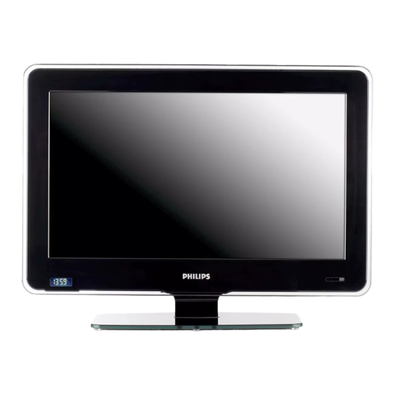
Philips 26HFL3350D/10 Service Manual

Philips 26HFL3350D/10 Service Manual

Chassis q522.2he la
Hide thumbs Also See for 26HFL3350D/10:

Advertisement

Colour Television
Contents
Connections
Wiring Diagram 26" Smartcard Alt BOM 2 (ME8)56
Wiring Diagram 32" Smartcard Alt BOM 1 (ME8)57
Wiring Diagram 32" Smartcard Alt BOM 2 (ME8)58
i Board (Part 1)
i Board (Part 2)
©
Copyright 2010 Koninklijke Philips Electronics N.V.
All rights reserved. No part of this publication may be reproduced, stored in a
retrieval system or transmitted, in any form or by any means, electronic, mechanical,
photocopying, or otherwise without the prior permission of Philips.
Published by MB/CC 1061 BU TV Consumer Care
Page
2
2
6
10
39
41
43
53
54
59
60
61
62
63
66
69
70
Drawing PWB
71
72-102
106-111
103
104
105
112
112
113
113
(HC01)
114
116
(HC02)
114
116
Printed in the Netherlands
Contents
IR & LED Panel v.3
System Interface Panel
Subject to modification
Chassis
Q522.2HE
LA
ME8
ME8
I_18030_000.eps
Page
(J)
117
118
119
120
(SI)
121
122-123
EN 3122 785 18035
031108

Advertisement

Table of Contents
loading

Summary of Contents for Philips 26HFL3350D/10

  • Page 1: Table Of Contents

    All rights reserved. No part of this publication may be reproduced, stored in a retrieval system or transmitted, in any form or by any means, electronic, mechanical, photocopying, or otherwise without the prior permission of Philips. Published by MB/CC 1061 BU TV Consumer Care...
  • Page 2: Revision List

    Here is product information available, as well as getting started, user manuals, frequently asked questions and software & drivers. Table 2-1 Described Model numbers Styling Published in: 26HFL3350D/10 3122 785 18030 26HFL5850D/10 3122 785 18030 32HFL3350D/10 3122 785 18030 32HFL5850D/10...
  • Page 3 Technical Specifications, Directions for Use, and Connections Q522.2HE LA EN 3 Connections OPTIONAL I_18030_001.eps 090602 Figure 2-1 Connection overview Note: The following connector colour abbreviations are used - Audio R 0.5 V / 10 kΩ (acc. to DIN/IEC 757): Bk= Black, Bu= Blue, Gn= Green, Gy= - Audio L 0.5 V / 1 kΩ...
  • Page 4 EN 4 Q522.2HE LA Technical Specifications, Directions for Use, and Connections 16 - Status/FBL 0 - 0.4 V: INT - POR Signal 1 - 3 V: EXT / 75 Ω - TV Clock Clock Signal 17 - Ground Video - Data in Data 18 - Ground FBL - Data out...
  • Page 5 Technical Specifications, Directions for Use, and Connections Q522.2HE LA EN 5 13 - Mini Jack: Bathroom speaker (Output) (optional) 17 - S-Video (Hosiden): Video Y/C - In Bk - Bathroom speaker 8 Ω / 1 W - Ground Y - Ground C / 75 Ω...
  • Page 6: Precautions, Notes, And Abbreviation List

    3.3.3 Spare Parts external damage. • Check the strain relief of the Mains/AC Power cord for For the latest spare part overview, consult your Philips Spare proper function. Part web portal. • Check the electrical DC resistance between the Mains/AC...
  • Page 7 Precautions, Notes, and Abbreviation List Q522.2HE LA EN 7 The third digit in the serial number (example: Abbreviation List AG2B0335000001) indicates the number of the alternative B.O.M. (Bill Of Materials) that has been used for producing the 0/6/12 SCART switch control signal on A/V specific TV set.
  • Page 8 6.5 MHz. L' is Band (VESA standard for communication I, L is all bands except for Band I channel and display). Using E-DDC, LG.Philips LCD (supplier) the video source can read the EDID Loudspeaker information form the display.
  • Page 9 SOPS Self Oscillating Power Supply Serial Peripheral Interface bus; a 4- wire synchronous serial data link standard S/PDIF Sony Philips Digital InterFace SRAM Static RAM Service Reference Protocol Small Signal Board Spread Spectrum Clocking, used to reduce the effects of EMI...
  • Page 10: Mechanical Instructions

    Figures below can deviate slightly from the actual situation, 4.3 Assy/Panel Removal ME8 Styling due to the different set executions. 4.4 Set Re-assembly Cable Dressing I_18030_005.eps 100108 Figure 4-1 Cable dressing 26HFL3350D/10 Alt BOM 1 (without integrated card slot) 2010-Jun-30...
  • Page 11 Mechanical Instructions Q522.2HE LA EN 11 I_18030_058.eps 100108 Figure 4-2 Cable dressing 26HFL5850D/10 Alt BOM 1 (with integrated card slot) 18035_101_100108.eps 100108 Figure 4-3 Cable dressing 26HFL5850D/10 Alt BOM 2 (with integrated card slot) 2010-Jun-30...
  • Page 12 EN 12 Q522.2HE LA Mechanical Instructions I_18030_009.eps 100108 Figure 4-4 Cable dressing 32HFL3350D/10 Alt BOM 1 (without integrated card slot) 18035_100_100108.eps 100108 Figure 4-5 Cable dressing 32HFL5850D/10 Alt BOM 2 (with integrated card slot) 2010-Jun-30...
  • Page 13 Mechanical Instructions Q522.2HE LA EN 13 I_18030_063.eps 100108 Figure 4-6 Cable dressing 32HFL5850D/10 Alt BOM 1 (with integrated card slot) 18030_100_090603.eps 100108 Figure 4-7 Cable dressing 42HFL5850D/10 (with integrated card slot) 2010-Jun-30...
  • Page 14 EN 14 Q522.2HE LA Mechanical Instructions Service Positions 4.3.2 Speakers The speakers are located in the backcover. The spring clips For easy servicing of this set, there are a few possibilities that ensure the electrical connection of the speakers to the created: SSB should be removed first.
  • Page 15 Mechanical Instructions Q522.2HE LA EN 15 I_18030_068.eps I_18030_070.eps 041108 041108 Figure 4-10 SSB wiring bottom-left Figure 4-12 iBoard wiring Figure 4-12 indicates the detailed positioning of the connectors to the iBoard. It applies to the 26HFL5850D/10. For all other sets, check positioning of the connectors before unplugging! 4.3.9 DC/DC Converter Panel 1.
  • Page 16 EN 16 Q522.2HE LA Mechanical Instructions I_18030_071.eps 041108 Figure 4-13 LCD Panel removal 26HFL5850D/10 (with integrated card slot) Set Re-assembly To re-assemble the whole set, execute all processes in reverse order. Notes: • While re-assembling, make sure that all cables are placed and connected in their original position.
  • Page 17: Service Modes, Error Codes, And Fault Finding

    Service Modes, Error Codes, and Fault Finding Q522.2HE LA EN 17 5. Service Modes, Error Codes, and Fault Finding Index of this chapter: 5.3.1 Service Default Mode (SDM) 5.1 Test Points 5.2 Hotel mode Purpose 5.3 Service Modes • To create a pre-defined setting, to get the same 5.4 Stepwise Start-up measurement results as given in this manual.
  • Page 18 RC. Display Option Code Contents of SAM: • Hardware Information. 39mm – A. SW Version. Displays the software version of the PHILIPS main software (example: Q522E-1.2.3.4 = MODEL: 32PF9968/10 AAAAB_X.Y.W.Z). PROD.SERIAL NO: AG 1A0620 000001 • AAAA= the chassis name.
  • Page 19 Service Modes, Error Codes, and Fault Finding Q522.2HE LA EN 19 – SW Events. Not useful for Service purposes. In case complete CSM content to the USB stick. The file (Csm.txt) will of specific software problems, the development be saved in the root of the USB stick. This information can be department can ask for this information.
  • Page 20 EN 20 Q522.2HE LA Service Modes, Error Codes, and Fault Finding • 12NC Display. Shows the 12NC of the display. upgradeable, it will also be published on the Internet. • Head phone Volume. Gives the last status of the head Example: Q582E_1.2.3.4.
  • Page 21 Service Modes, Error Codes, and Fault Finding Q522.2HE LA EN 21 Mains Mains - WakeUp requested WakeUp requested - Acquisition needed Semi - No data Acquisition St by Active required St by - Tact SW pushed - St by requested - Last status is hibernate - Tact switch pushed - Tact SW pushed...
  • Page 22 EN 22 Q522.2HE LA Service Modes, Error Codes, and Fault Finding Off/Stby to Semi Stand by or Protection Mains is applied Standby Supply starts running. All standby supply voltages become available . st-by µP resets If the protection state was left by short circuiting the SDM pins, detection of a protection condition during startup will stall the startup.
  • Page 23 Service Modes, Error Codes, and Fault Finding Q522.2HE LA EN 23 (pulling pin of the probe interface to ground by inserting EJTAG probe) An EJTAG probe (e.g. WindPower ICE probe) can be connected for Linux Kernel debugging purposes. EJTAG probe connected ? Cold boot? Release AVC system reset...
  • Page 24 EN 24 Q522.2HE LA Service Modes, Error Codes, and Fault Finding Constraints taken into account: - Display may only be started when valid LVDS output clock can be delivered by the AVC . - Between 5 and 50 ms after power is supplied, display should receive valid LVDS clock . action holder: AVC - Backlight Control PWM output should always keep low until LVDS power is supplied .
  • Page 25 Service Modes, Error Codes, and Fault Finding Q522.2HE LA EN 25 action holder: AVC Active action holder: St-by autonomous action Mute all sound outputs via softmute Wait 100ms Set main amplifier mute (I/O: audio-mute) Force ext. audio outputs to ground (I/O: audio reset) and wait 5ms Switch “off”...
  • Page 26 EN 26 Q522.2HE LA Service Modes, Error Codes, and Fault Finding Semi Stand by If ambientlight functionality was used in semi -standby (lampadaire mode), switch “off” ambient light *) If this is not performed and the set is Delay transition until ramping down of ambient light is switched to standby when the switch “off”...
  • Page 27 Service Modes, Error Codes, and Fault Finding Q522.2HE LA EN 27 action holder: MIPS action holder: St-by autonomous action Log the appropriate error and set stand-by flag in NVM Redefine wake up reasons for protection state and transfer to stand-by µP. Switch “off”...
  • Page 28 EN 28 Q522.2HE LA Service Modes, Error Codes, and Fault Finding supply detection algorithms for DC-DC outputs DETECT 1 = Low ? Polling every 40ms Check DETECT1 5 times ( within 500us ) DETECT 1 = Low ? 5 consecutive times ? Shutdown ( Active to Semistdby to standby ) Wait for 5 seconds...
  • Page 29 Service Modes, Error Codes, and Fault Finding Q522.2HE LA EN 29 +12V supply detection algorithm Polling every 40ms DETECT 2 = Low ? Check DETECT2 5 times ( within 500us) DETECT 2 = Low ? 5 consecutive times ? Shutdown ( Active to Semistdby to standby ) Wait for 5 seconds Restart...
  • Page 30 Support of the LVDS Tool has been discontinued. 5.5.1 ComPair Introduction Error Codes ComPair (Computer Aided Repair) is a Service tool for Philips Consumer Electronics products. and offers the following: 5.6.1 Introduction 1. ComPair helps to quickly get an understanding on how to repair the chassis in a short and effective way.
  • Page 31 Service Modes, Error Codes, and Fault Finding Q522.2HE LA EN 31 content, as this history can give significant information). This to cause the "PROT-DC" (B02C) line activated. Or another ensure that old error codes are no longer present. possibility is the 12V supply under voltage cause the If possible, check the entire contents of the error buffer.
  • Page 32 EN 32 Q522.2HE LA Service Modes, Error Codes, and Fault Finding The Blinking LED Procedure Protections 5.7.1 Introduction 5.8.1 Software Protections The blinking LED procedure can be split up into two situations: Most of the protections and errors use either the stand-by •...
  • Page 33 Service Modes, Error Codes, and Fault Finding Q522.2HE LA EN 33 Fault Finding and Repair Tips 1. Check the drop voltage across resistor 3U70 or 3U3T (they could be too high, meaning a defective controller IC or MOS-FETs). Read also section Extra Information.
  • Page 34 Before starting: - prepare a USB memory stick with the latest software - download the latest Main Software (Fus) from www.p4c.philips.com - unzip this file - create a folder ”upgrades” in the root of a USB stick (size > 50 MB) and save the autorun.upg file in this "upgrades"...
  • Page 35 Service Modes, Error Codes, and Fault Finding Q522.2HE LA EN 35 Set is st art in g u p in F act o ry m o d e Set is starting up in F actory m ode? Noisy picture with bands/lines is visible and the An “F”...
  • Page 36 EN 36 Q522.2HE LA Service Modes, Error Codes, and Fault Finding 5.9.5 Display option code Caution: In case the SSB has been replaced, always check the display option code in SAM, even if a picture is shown. With a wrong display option code it is possible that a picture is shown, but that in certain conditions unwanted side-effects could occur.
  • Page 37 1. Disconnect the TV from the Mains/AC Power. software, use the following steps: 2. Press the “OK” button on a Philips DVD RC-6 remote 1. Disconnect the TV from the Mains/AC Power. control (it is also possible to use the TV remote in “DVD”...
  • Page 38 EN 38 Q522.2HE LA Service Modes, Error Codes, and Fault Finding 5.10.4 Content and Usage of the One-Zip Software File Below a content explanation of the One-Zip file is shown (content may vary per chassis), and instructions on how and when to use it.
  • Page 39: Alignments

    Alignments Q522.2HE LA EN 39 6. Alignments Index of this chapter: • Switch the set to stand-by mode. 6.1 General Alignment Conditions 6.2 Hardware Alignments For the next alignments, supply the following test signals via a 6.3 Software Alignments video generator to the RF input: 6.4 Option Settings •...
  • Page 40 6.4.5 Option Code Overview Table 6-4 Option code overview (subject to change and as available at time of publishing) CTN MODEL Displ. code Group 1 Group 2 Alt BOM Panel Type 26HFL3350D/10 41472 04109 06223 12328 08872 00101 00000 00000...
  • Page 41: Circuit Descriptions

    Circuit Descriptions Q522.2HE LA EN 41 7. Circuit Descriptions Index of this chapter: The hospitality-specific features comprise: 7.1 Introduction • Advanced Hotel mode (volume lock, front control lock out, 7.2 Main Power Supply guest menu, welcome message, etc.) • Integrated LCD clock display with wake-up alarm •...
  • Page 42 EN 42 Q522.2HE LA Circuit Descriptions 7.1.2 SSB Cell Layout 1P36, (BDS HDMI) I_18010_079.eps 091127 Figure 7-2 SSB layout cells (top view) Main Power Supply 7.2.1 Specifications For an overview of the output voltages of the Power Supplies, There are two types of the power supply used in the TV522 refer to the wiring diagrams in chapter Block Diagrams.
  • Page 43: Ic Data Sheets

    IC Data Sheets Q522.2HE LA EN 43 8. IC Data Sheets This section shows the internal block diagrams and pin configurations of ICs that are drawn as “black boxes” in the electrical diagrams (with the exception of “memory” and “logic” ICs).
  • Page 44 EN 44 Q522.2HE LA IC Data Sheets Diagram B02C SSB: DC / DC, ST1S10PHD (IC 7U0Z) Block diagram Pinning information DFN8 (4 × 4) PowerSO-8 I_18010_083.eps 100402 Figure 8-2 Internal block diagram and pin configuration 2010-Jun-30...
  • Page 45 IC Data Sheets Q522.2HE LA EN 45 Diagram B03A SSB: Main Tuner, TDA9898HL (IC 7T57) Block Diagram 4 MHz reference input EXTERNAL SOUND BAND-PASS FILTER i.c. ADRSEL GNDD LFSYN2 GNDA EXTFILO EXTFILI FREF OPTXTAL 43, 44 40, 41 C-BUS SYNTHESIZER 4 MHz FREQUENCY SUPPLY AND VCO...
  • Page 46 EN 46 Q522.2HE LA IC Data Sheets Diagram B03B SSB: Channel Decoder DVB-T, TDA10048HN (IC7T17-1) Block Diagram AGC_TUN AGC_IF ANALOG ΣΛ STEP INTERFACE DIGITAL FRONT-END DUAL CHANNEL ESTIMATION AND OFDM AND CORRECTION DEMODULATION ΣΛ STEP INTERFACE DIGITAL DYNAMIC 2K / 4K / 8K TIMESHIFT CANCELLER PARTIAL...
  • Page 47 IC Data Sheets Q522.2HE LA EN 47 Diagram B04x SSB: PNX8541: Standby Controller, PNX85xx (IC 7H00) Block Diagram DDR-II DDR-II 32 MB 32 MB PNX85xx Matrix Display 1368 × 768 A/V INPUTS MIPS32@240MHz TV control, Pixel OSD Source select 3D-Comb Digital color decoder Audio decoding Full audio processing, inc SRS...
  • Page 48 EN 48 Q522.2HE LA IC Data Sheets Diagram B04M SSB: PNX8541: Audio, TS4821DT (IC 7HV3) Typical Application Schematic Rfeed1 Rfeed1 1µF 1µF 3.9k 3.9k Rpol Rpol 100k 100k Right In Right In Cin1 Cin1 3.9k 3.9k 220µF 220µF RL=32Ohms RL=32Ohms Rin1 Rin1 2.2µF...
  • Page 49 IC Data Sheets Q522.2HE LA EN 49 Diagram B05A SSB: Dual LVDS, BU7988KVT (IC 7CG0) Block Diagram Pin Configuration I_17970_059.eps 060608 Figure 8-7 Internal block diagram and pin configuration 2010-Jun-30...
  • Page 50 EN 50 Q522.2HE LA IC Data Sheets Diagram B08A SSB: Digi IO: USB, ISP1564HL (IC 7P00) Block Diagram PME# 77, 98, 100 CC(IO)AUX GLOBAL CONTROL 10, 12 to 15, 20 to 22, AD[31:0] 26 to 31, 33, 34, 50 to 54, 56, 57, PCI CORE VOLTAGE 59, 62, 63, 65 to 70...
  • Page 51 IC Data Sheets Q522.2HE LA EN 51 Diagram B08C SSB: Digi IO: HDMI MUX, AD8197A (IC 7P70) Block Diagram Figure 1. TYPICAL APPLICATION 04:20 Pin Configuration AVCC AVCC PIN 1 INDICATOR IN_B0 IP_C3 IP_B0 IN_C3 AVEE AVEE IN_B1 IP_C2 IP_B1 IN_C2 VTTI VTTI...
  • Page 52 EN 52 Q522.2HE LA IC Data Sheets 8.10 Diagram B10A SSB: Digi IO: Class-D, TDA8932B (IC 7D10) Block Diagram BOOT1 OSCILLATOR DDP1 IN1P DRIVER HIGH OUT1 CTRL MODULATOR DRIVER SSP1 IN1N MANAGER BOOT2 INREF DDP2 IN2P DRIVER HIGH OUT2 CTRL MODULATOR DRIVER SSP2...
  • Page 53: Block Diagrams

    Block Diagrams Q522.2HE LA EN 53 9. Block Diagrams Wiring Diagram 26" & 32" Alt BOM 1(ME8) WIRING DIAGRAM 26"- 32" ALT BOM 1 (STYLING ME8) LCD DISPLAY (1004) LVDS INPUT INVERTER 1G50 (B06A) 41. VDISP (1150) 40. VDISP 14. ANALOG_PWM 39.
  • Page 54: Wiring Diagram 26" Alt Bom 2 (Me8)

    Block Diagrams Q522.2HE LA EN 54 Wiring Diagram 26" Alt BOM 2 (ME8) WIRING DIAGRAM 26" ALT BOM 2 (STYLING ME8) LCD DISPLAY (1004) LVDS INPUT 8401 1G50 (B06A) 41. VDISP (1150) 40. VDISP 39. VDISP 8G50 38. VDISP DANGEROUS DANGEROUS HIGH VOLTAGE HIGH VOLTAGE...
  • Page 55: Wiring Diagram 26" Smartcard Alt Bom 1 (Me8)55

    Block Diagrams Q522.2HE LA EN 55 Wiring Diagram 26" Smartcard Alt BOM 1 (ME8) WIRING DIAGRAM 26" WITH INTEGRATED SMARTCARD SLOT ALT BOM 1 (STYLING ME8) DC/DC CONVERTER 8100 1102 (HC01) INTEGRATED SMARTCARD SLOT iBOARD (1184) 8109 (1182) 8101 8D11 8208 8104 8CN8...
  • Page 56 Block Diagrams Q522.2HE LA EN 56 Wiring Diagram 26" Smartcard Alt BOM 2 (ME8) WIRING DIAGRAM 26" WITH INTEGRATED SMARTCARD SLOT ALT BOM 2 (STYLING ME8) DC/DC CONVERTER 8100 1102 (HC01) INTEGRATED SMARTCARD SLOT iBOARD (1184) 8109 (1182) 8101 8D11 8208 8104 8CN8...
  • Page 57 Block Diagrams Q522.2HE LA EN 57 Wiring Diagram 32" Smartcard Alt BOM 1 (ME8) WIRING DIAGRAM 32" WITH INTEGRATED SMARTCARD SLOT ALT BOM 1 (STYLING ME8) 8CN8 8109 8101 INTEGRATED 8D11 SMARTCARD SLOT (1184) 1110 1109 1207 (HC01) (HC01) (HC02) 1208 (HC02) iBOARD...
  • Page 58 Block Diagrams Q522.2HE LA EN 58 Wiring Diagram 32" Smartcard Alt BOM 2 (ME8) WIRING DIAGRAM 32" WITH INTEGRATED SMARTCARD SLOT ALT BOM 2 (STYLING ME8) 8CN8 8109 8101 INTEGRATED 8D11 SMARTCARD SLOT (1184) 1110 1109 1207 (HC01) (HC01) (HC02) 1208 (HC02) iBOARD...
  • Page 59: Wiring Diagram 42" Smartcard (Me8)

    Block Diagrams Q522.2HE LA EN 59 Wiring Diagram 42" Smartcard (ME8) WIRING DIAGRAM 42" WITH INTEGRATED SMARTCARD SLOT (STYLING ME8) 8402 8101 DC/DC CONVERTER 8E0A 8100 iBOARD 1102 (HC01) (1182) LCD DISPLAY (1004) INTEGRATED LVDS INPUT (1080p) SMARTCARD SLOT (1184) 8401 1205 (HC02)
  • Page 60: Block Diagram Video

    Block Diagrams Q522.2HE LA EN 60 Block Diagram Video VIDEO B03A B05A B06A MAIN TUNER PNX8541 DUAL LVDS LVDS 7H00 7T57 1T04 PNX8541E/M1 TDA9898HL TD1716F/BHXP 1T55 7T56 B04K ANALOGUE AV IF-FILTP1 1G50 IF1-A B04O DIGITAL 7CG0 CVBS4 CVBS VIDEO OUT BU7988KVT VDISP MAIN HYBRID...
  • Page 61: Block Diagram Audio

    Block Diagrams Q522.2HE LA EN 61 Block Diagram Audio AUDIO B03A B04Q MAIN TUNER PNX8541 PNX8541 PNX8541: FLASH 7T57 7H00 1T04 TDA9898HL PNX8541E/M1 TD1716F/BHXP 1T55 7T56 IF-FILTP1 B04K ANALOGUE AV IF1-A CVBS4 CVBS MAIN HYBRID IF-FILTN1 IF1-B TUNER SAW 37MHZ67 PROCESSING 1T70 7HA0...
  • Page 62: Block Diagram Control & Clock Signals

    Block Diagrams Q522.2HE LA EN 62 Block Diagram Control & Clock Signals CONTROL + CLOCK SIGNALS B02B DC/DC +3V3-STANDBY_+1V2-STANDBY B04G PNX 8541: DDR2 PNX8541 B03B CHANNEL DECODER DVB-T B03A MAIN TUNER 7T57 1T04 7H00 TDA9898HL TD1716F PNX8541E B04N VIDEO STREAMS MAIN PROCESSING TUNER...
  • Page 63: Ssb: Test Points (Overview Top Side)

    Block Diagrams Q522.2HE LA EN 63 SSB: Test Points (Overview Top Side) IGBC A1 IGBD A1 IH06 IHBT B3 IHBU B3 IHPF C3 IHR0 C3 IHR2 C3 IHR3 C3 IHR4 C3 IHR5 C3 IHR6 C3 IHR7 C3 IHRC C3 IHRF C3 IHRH C3 IHSF C3 Part 1...
  • Page 64 Block Diagrams Q522.2HE LA EN 64 SSB: Test Points (Part 1 Top Side) Part 1 I_18010_046a.eps 040608 2010-Jun-30...
  • Page 65 Block Diagrams Q522.2HE LA EN 65 SSB: Test Points (Part 2 Top Side) Part 2 I_18010_046b.eps 040608 2010-Jun-30...
  • Page 66: Ssb: Test Points (Overview Bottom Side)

    Block Diagrams Q522.2HE LA EN 66 SSB: Test Points (Overview Bottom Side) 1U21 FEB8 FP48 ID53 IHC6 IHYA IT15 AH00 FEB9 FP49 IE00 IHC7 IHYB IT16 AT62 FG00 FP4A IE01 IHC8 IHYC IT17 AT63 FG01 FP4B IE02 IHD0 IHYD IT18 AT64 FG02 FP4C...
  • Page 67 Block Diagrams Q522.2HE LA EN 67 SSB: Test Points (Part 1 Bottom Side) Part 1 I_18010_055a.eps 040608 2010-Jun-30...
  • Page 68 Block Diagrams Q522.2HE LA EN 68 SSB: Test Points (Part 2 Bottom Side) Part 2 I_18010_055b.eps 040608 2010-Jun-30...
  • Page 69: I2C Ic Overview

    Block Diagrams Q522.2HE LA EN 69 I2C IC Overview I²C B04E PNX8541: CONTROL_MIPS B08C DIGI I/O: HDMI MUX B08B DIGI I/O: HDMI CONNECTORS + DVI AUDIO INPUTS B03B CHANNEL DECODER DVB-T B03A MAIN TUNER 7H00 +3V3-PER PNX8541E 3HPJ AJ27 SDA3 SDA-SSB I2C3-SDA 3HPH...
  • Page 70: Supply Lines Overview

    Block Diagrams Q522.2HE LA EN 70 Supply Lines Overview SUPPLY LINES OVERVIEW DUAL DC CONVERTER SUPPLY B02B DC/DC +3V3-STANDBY B04I B07A ANALOGUE I/O: SCART 1 & 2 B02C DC/DC PNX8541: AUDIO +1V2-STANDBY +3V3 +3V3 1001 +AUDIO-POWER +AUDIO-POWER B02b +12V +12V +12V B02a 5HM0...
  • Page 71: Circuit Diagrams And Pwb Layouts

    Circuit Diagrams and PWB Layouts Q522.2HE LA EN 71 10. Circuit Diagrams and PWB Layouts Main Supply Panel (42") MAIN SUPPLY PANEL (42") I_18011_014.eps 020609 2010-Jun-30...
  • Page 72: Small Signal Board (B02-B10)

    Circuit Diagrams and PWB Layouts Q522.2HE LA EN 72 SSB: DC / DC 3V3 1V2 2U00 D5 2U07 D9 2U0E G2 2U0N A2 2U0Z B9 2U16 D12 3U06 C6 3U0F G1 3U0P B5 3U0Y E10 3U15 C7 3U1D F11 3U1M B8 3U70 A4 3U77 B2 6U02 A3...
  • Page 73 Circuit Diagrams and PWB Layouts Q522.2HE LA EN 73 SSB: DC / DC +3V3 +1V2 Standby 1M95 D2 1M99 B2 2U22 E3 DC / DC +3V3-STANDBY +1V2-STANDBY B02B B02B 2U23 E3 2U24 D5 2U25 D6 2U26 E7 2U51 C3 2U52 C3 2U53 C3 2U54 C3 2U55 D3...
  • Page 74 Circuit Diagrams and PWB Layouts Q522.2HE LA EN 74 SSB: DC / DC 1U21 D3 DC / DC 2U90 B2 B02C B02C 2U91 B2 2U92 B2 2U93 B5 2U94 B5 2U95 B5 2U96 B5 2U97 C3 3U80 B3 3U81 B5 3U82 B5 3U83 B5 3U84 B6...
  • Page 75 Circuit Diagrams and PWB Layouts Q522.2HE LA EN 75 SSB: Main Tuner 1T04 D2 1T75 B5 2T47 G8 2T5B B9 2T62 F5 2T66 G14 2T73 G13 2T78 F13 2T82 H10 2T87 F9 2T96 F13 3T25 G9 3T40 G10 3T55 H10 3T5B B7 3T5F C8 3T74 H10...
  • Page 76 Circuit Diagrams and PWB Layouts Q522.2HE LA EN 76 SSB: Channel Decoder DVB-T 2T01 A8 2T07 C8 2T12 C11 2T15 C12 2T19 D8 2T24 F6 2T27 B8 2T31 D2 2T36 C9 3T06 D8 3T09 D7 3T13 C2 3T18 G8 3T21 D3 3T29 G8 3T32 G13 5T09 A8...
  • Page 77 Circuit Diagrams and PWB Layouts Q522.2HE LA EN 77 SSB: PNX8541: Standby Controller 1H00 A4 FH02 G13 2H00 B3 FH03 C13 PNX 8541: STANDBY CONTROLLER 2H01 D3 FH04 E8 B04A B04A 2H02 A3 FH05 E6 2H03 F6 IH00 D10 2H04 A3 IH01 D11 2H06 C14 IH02 D4...
  • Page 78 Circuit Diagrams and PWB Layouts Q522.2HE LA EN 78 SSB: PNX8541: NVM 2HC0 A5 PNX 8541: NVM 2HC1 C7 B04B B04B 3HC2-1 A3 +3V3-PER 3HC2-2 A4 IHC2 3HC2-3 B5 3HC7 F6 3HC8 F5 3HC9 B4 5HC0 C6 FHC9 FHC6 3HC2-1 6HC1 C6 RESET-NVM_WP-NANDFLASH BC857BW...
  • Page 79 Circuit Diagrams and PWB Layouts Q522.2HE LA EN 79 SSB: PNX8541: Miscellaneous 2HD0 C3 3HD3-1 B2 PNX 8541: MISCELLANEOUS B04C B04C 3HD3-2 C2 3HD3-3 D2 3HD3-4 B4 7HD0 B3 FHD0 B4 FHD1 C2 IHD0 C3 +3V3-STANDBY +3V3-STANDBY FHD0 RESET-STBY 7HD0 NCP303LSN10T1 FHD1 IHD0...
  • Page 80 Circuit Diagrams and PWB Layouts Q522.2HE LA EN 80 SSB: PNX8541: Control MIPS 2HF2 C1 +3V3-PER +3V3-PER 2HF5 C7 PNX8541: CONTROL MIPS B04E B04E 2HF6 C7 2HF7 D8 2HF8 D8 2HP1 E5 3HF0 B5 3HF1 D2 IHFC 3HF2 C6 7H00-4 3HF3 A6 PNX8541E1/M1/2414 3HF4 C6...
  • Page 81 Circuit Diagrams and PWB Layouts Q522.2HE LA EN 81 SSB: PNX8541: Control PCI 3HE5 B2 3HED-1 B7 PNX 8541: CONTROL PCI B04F B04F 3HED-2 B8 3HED-3 B8 3HED-4 B7 3HEE-1 B7 3HEE-2 C8 3HEE-3 B7 3HES-1 C7 3HES-2 C7 3HES-3 D7 3HES-4 D7 3HEU C5 7H00-5 B4...
  • Page 82 Circuit Diagrams and PWB Layouts Q522.2HE LA EN 82 SSB: PNX8541: DDR2 2HG0 E2 3HJ4 B13 PNX 8541: DDR2 2HG1 E3 3HJ5 A4 B04G B04G 2HG2 E3 3HJV B4 3HJ5 IHG0 2HG3 E3 3HJW B5 7H00-2 PNX8541E1/M1/2414 2HG4 E3 3HJY A4 +1V8-PNX8541 +1V8-PNX8541 +1V8-PNX8541...
  • Page 83 Circuit Diagrams and PWB Layouts Q522.2HE LA EN 83 SSB: PNX8541: Digital Video In Personal Notes: 3HK0 D2 PNX 8541: DIGITAL VIDEO IN 7H00-3 B2 B04H B04H 9HK0 C2 IHKM D2 7H00-3 PNX8541E1/M1/2414 HDMI RX2- RX2+ RX_0 HOT-PLUG HOT_PLUG RX1- RX_1 RX1+ RX0-...
  • Page 84 Circuit Diagrams and PWB Layouts Q522.2HE LA EN 84 SSB: PNX8541: Audio 2HM3 C4 2HM4 C6 PNX 8541: AUDIO B04I B04I 2HM5 F6 2HM8 F4 2HMG C3 2HMH D3 2HMJ A10 2HMN B10 2HMP B10 AUDIO-VDD 2HMT D10 2HMW F10 2HMY H9 2HMJ IHMY...
  • Page 85 Circuit Diagrams and PWB Layouts Q522.2HE LA EN 85 SSB: PNX8541: Analogue AV 2HA2 C2 IHPA G8 2HS4 IHSF 3HRS 2HA3 C3 IHPB F9 PNX 8541: ANALOGUE AV SC1-CVBS B04K B04K 2HA4 D3 IHPC G9 2HA5 D3 IHPD G11 2HKL F3 IHPF A7 2HRZ A7 IHPG H8...
  • Page 86 Circuit Diagrams and PWB Layouts Q522.2HE LA EN 86 SSB: PNX8541: Audio 2HB0 B4 IHBK E3 2HB1 B4 IHBL E4 PNX 8541: AUDIO 2HB2 B4 IHBM E4 B04L B04L 2HB3 B4 IHBT D3 2HB4 B4 IHBU D3 2HB5 C4 IHBV D3 2HB6 C4 IHBW C3 2HB7 C4...
  • Page 87 Circuit Diagrams and PWB Layouts Q522.2HE LA EN 87 SSB: PNX8541: Audio 1HV1 E4 IHVR B6 2HVG E6 IHVS C6 2HVL A3 IHVT B5 PNX 8541: AUDIO B04M B04M 2HVM B1 IHVZ D2 2HVN B5 2HVO B4 2HVP B3 2HVQ B4 2HVR C1 2HVS C5 2HVL...
  • Page 88 Circuit Diagrams and PWB Layouts Q522.2HE LA EN 88 SSB: PNX8541: Video Streams 3HWM C8 PNX 8541: VIDEO STREAMS 3HWN C7 B04N B04N 3HWP C8 3HWR C7 3HWS B8 3HWT B7 3HWU B8 9HY0 3HWV B7 3HWZ CA-MDI0 3HWW B8 9HY1 3HWY A7 3HWY...
  • Page 89 Circuit Diagrams and PWB Layouts Q522.2HE LA EN 89 SSB: PNX8541: Power 2HH6 B5 2HH7 C5 PNX 8541: POWER 2HH8 C5 B04P B04P 2HH9 B5 2HK1 B3 2HK2 E2 2HK4 E1 2HK6 E4 7H00-11 2HK7 C2 PNX8541E1/M1/2414 2HK8 C3 IHY6 2HKA C1 +1V2-PNX8541 5HY3...
  • Page 90 Circuit Diagrams and PWB Layouts Q522.2HE LA EN 90 SSB: PNX8541: Flash 2HA0 B7 PNX 8541: FLASH 2HA1 B7 B04Q B04Q 3HA0 B2 3HA1 C9 3HA3 B9 3HA4-1 B4 3HA4-2 B4 3HA4-3 C4 3HA4-4 C4 3HA8-1 C4 3HA8-2 C4 3HA8-3 C4 3HA8-4 C4 3HAC-1 E4 3HAC-2 D4...
  • Page 91 Circuit Diagrams and PWB Layouts Q522.2HE LA EN 91 SSB: Dual LVDS 2CG0 B7 2CG1 B7 DUAL LVDS 2CG2 B7 B05A B05A 2CG3 B7 2CG4 B7 2CG5 B9 2CG6 B8 2CG7 B9 2CG8 B8 2CG9 C8 2CGA C10 +3V3 +3V3 +3V3 3CG0 C6 3CG1 C6...
  • Page 92 Circuit Diagrams and PWB Layouts Q522.2HE LA EN 92 SSB: LVDS 1G50 A13 LVDS 1G54 C9 B06A B06A 1G55 C9 1G56 D9 1G57 D9 1G58 E9 1G59 E9 1G60 F9 1G61 F9 1G62 G9 1G63 G9 FOR SINGLE LVDS ONLY 1G64 H9 1G50 FX15SC-41S-0.5SH...
  • Page 93 Circuit Diagrams and PWB Layouts Q522.2HE LA EN 93 SSB: Display Interfacing 1GA0 B1 2G54 B5 2G57 C2 DISPLAY-INTERFACING B06B B06B 2G58 F12 2G60 D5 2G63 F5 2G64 F5 2G65 F5 2G66 F5 2G76 C4 3G55 E13 3G56 B4 3G60 D3 3G62 E11 FOR ITV 3G63 C2...
  • Page 94 Circuit Diagrams and PWB Layouts Q522.2HE LA EN 94 SSB: Analog IO: Scart 1 & 2 1001 E11 6E22 E12 1009 B12 6E23 D12 ANALOG IO: SCART 1 & 2 B07A B07A 1011 G6 6E24 D6 1015 C12 6E26 F12 1022 A6 6E28 G12 1023 B6...
  • Page 95 Circuit Diagrams and PWB Layouts Q522.2HE LA EN 95 SSB: Analog IO: YPbPr Audio Out 1E03 B1 IE00 F2 1E08-1 C10 IE01 E9 ANALOG IO: YPbPr AUDIO OUT 1E08-2 A10 IE02 E9 B07B B07B 1E08-3 B10 IE03 G2 1E09 C12 IE07 H9 1E0A F1 IE15 C7...
  • Page 96 Circuit Diagrams and PWB Layouts Q522.2HE LA EN 96 SSB: Analog IO: Side AV 1000 F3 1002 E3 ANALOG IO: SIDE AV B07C B07C 1003 D3 1004 C3 1005 B3 1006 B3 1007 A3 1010 F4 RESERVED 9E13 1E11-1 C2 FRONT-C 1E11-2 C2 9E14...
  • Page 97 Circuit Diagrams and PWB Layouts Q522.2HE LA EN 97 SSB: Analog IO: Bolt On 1008 C12 IEBA F3 1029 D12 IEBB E2 ANALOG IO: BOLT - ON 1E06 C13 IEBE F3 B07D B07C 1E50 C13 1HE0 A1 1HP0 C1 1R06 D1 1R07 C1 3E39-4 EJTAG-TRSTN...
  • Page 98 Circuit Diagrams and PWB Layouts Q522.2HE LA EN 98 SSB: Digi IO: USB 1P01 D6 DIGI IO: USB CONNECTOR + CONTROLLER 1P07 C13 B08A B08A 2P00 D9 2P01 D9 2P02 D10 2P03 C7 2P04 D6 2P05 D6 2P06 D6 5P04 2P07 D6 2P08 D7 2P09 E10...
  • Page 99 Circuit Diagrams and PWB Layouts Q522.2HE LA EN 99 SSB: Digi IO: HDMI & DVI 1P32 A8 7P44 B11 1P33 A1 7P4P G12 DIGI IO: HDMI CONNECTORS + DVI AUDIO INPUTS 1P34 E8 7P4Q I9 6P41 B08B B08B 1P35 E1 7P4R I9 1P36 C8 9P30 A4...
  • Page 100 Circuit Diagrams and PWB Layouts Q522.2HE LA EN 100 SSB: Digi IO: HDMI MUX 2P70 E6 2P71 F6 B08C B08C DIGI IO: HDMI MUX 2P72 E7 2P73 F7 2P74 F7 2P75 F7 2P76 F7 2P77 F7 2P78 E7 2P79 F7 2P7A F8 2P7B F8 2P7C F8...
  • Page 101 Circuit Diagrams and PWB Layouts Q522.2HE LA EN 101 SSB: Digi IO: PCMCIA Interf. & Buffer 1N00-A B2 DIGI IO: PCMCIA INTERFACE & BUFFER 1N00-B E2 B09A B09A 1N01 H2 IN2M 5N01 2N01 A7 +3V3_BUF +3V3 2N02 A7 2N03 B7 2N05 B1 2N20 A12 IM2N...
  • Page 102 Circuit Diagrams and PWB Layouts Q522.2HE LA EN 102 SSB: Digi IO: Class-D 1D10 B5 FD20 B7 1D12 E12 FD21 E4 CLASS D B10A B10A 2D10 B8 FD22 E11 2D11 B12 FD23 F11 2D12 B7 FD24 F11 2D14 B10 FD25 F3 2D16 C8 FD26 F11 2D17 C12...
  • Page 103: Ssb: Srp List Explanation

    Circuit Diagrams and PWB Layouts Q522.2HE LA EN 103 SSB: SRP List Explanation Example Personal Notes: 1 . 1 . Introduction Net Name Diagram +12-15V AP1 (4x) +12-15V AP4 (4x) SRP (Service Re ference Protocol) is a softw are too l that creates a list w i th all refer e n c es to signal lines. The list contains +12-15V AP5 (12x) +12-15V...
  • Page 104 Circuit Diagrams and PWB Layouts Q522.2HE LA EN 104 SSB: SRP List Part 1 Netname Diagram ADAC(4) B04M (2 ×) AV2-BLK B04A (1 ×) CA-MDO7 B09A (1 ×) DDR2-BA1 B04G (4 ×) DV-G0_UV2 B05A (2 ×) ADAC(5) B04I (1 ×) AV2-BLK B07A (1 ×) CA-MICLK...
  • Page 105 Circuit Diagrams and PWB Layouts Q522.2HE LA EN 105 SSB: SRP List Part 2 Netname Diagram PARX-DDC-SDA B08C (1 ×) PCI-AD4 B08A (1 ×) PROT-DC B02C (1 ×) SDA-SSB B03A (1 ×) TXOCLK+ B05A (1 ×) PBRX-DDC-SCL B08B (1 ×) PCI-AD4 B09A (1 ×) PSEN...
  • Page 106 Circuit Diagrams and PWB Layouts Q522.2HE LA EN 106 Layout Small Signal Board (Overview Top Side) 1000 A5 2D40 D1 2T5C D5 3HB0 B3 7D10 D2 1001 A5 2D41 D1 2T62 D4 3HB1 B3 7D13 E2 1002 A5 2D44 D2 2T64 D5 3HB2 B3 7D16 E1...
  • Page 107 Circuit Diagrams and PWB Layouts Q522.2HE LA EN 107 Layout Small Signal Board (Part 1 Top Side) Part 1 I_18010_042a.eps 030608 2010-Jun-30...
  • Page 108 Circuit Diagrams and PWB Layouts Q522.2HE LA EN 108 Layout Small Signal Board (Part 2 Top Side) Part 2 I_18010_042b.eps 030608 2010-Jun-30...
  • Page 109 Circuit Diagrams and PWB Layouts Q522.2HE LA EN 109 Layout Small Signal Board (Overview Bottom Side) 1H00 B3 2HA3 C3 2HU8 C3 2T01 C2 3E07 B1 3H00 C3 3HKR B4 3P4M E3 3U1R F5 6U01 E4 9P31 E3 1P3T D1 2HA4 C3 2HUB C3 2T03 C1...
  • Page 110 Circuit Diagrams and PWB Layouts Q522.2HE LA EN 110 Layout Small Signal Board (Part 1 Bottom Side) Part 1 I_18010_043a.eps 030608 2010-Jun-30...
  • Page 111 Circuit Diagrams and PWB Layouts Q522.2HE LA EN 111 Layout Small Signal Board (Part 2 Bottom Side) Part 2 I_18010_043b.eps 030608 2010-Jun-30...
  • Page 112: Dc / Dc Converter Panel

    Circuit Diagrams and PWB Layouts Q522.2HE LA EN 112 DC / DC Converter Panel Layout DC / DC Converter Panel (Top Side) 1001 D1 2005 B4 2012 B4 2018 A2 3006 C4 4002 D3 5003 B1 7002 C2 F105 C3 I105 B2 I111 B3 I117 C4...
  • Page 113: Keyboard Control Panel

    Circuit Diagrams and PWB Layouts Q522.2HE LA EN 113 Keyboard Control Panel Layout Keyboard Control Panel (Top Side) 1N10 A1 1N13 C3 1N16 C4 3N08 B1 3N12 B3 3N15 B4 6N10 B2 FN11 B1 IN12 B3 IN15 B4 1N11 C2 1N14 C4 2N10 B1 3N09 B2...
  • Page 114 Circuit Diagrams and PWB Layouts Q522.2HE LA EN 114 i Board (Part 1) 1100 G12 4111 D2 1101 A1 5101 A3 iBOARD (PART 1) 1102 A7 5102 A5 HC01 HC01 1104 E9 5103 B5 1107 D6 5104 B5 1108 E5 5105 C4 1109 D2 5106 C4...
  • Page 115 Circuit Diagrams and PWB Layouts Q522.2HE LA EN 115 i Board (Part 2) 1096 I13 3261 E2 F227 F2 1097 I12 3263 E4 F228 F14 iBOARD (PART 2) 1098 I12 3264 E9 F229 F14 HC02 HC02 1099 I11 3265 A3 F230 F14 1200 A1 3266 A3...
  • Page 116 Circuit Diagrams and PWB Layouts Q522.2HE LA EN 116 Layout i Board (Top Side) Layout i Board (Bottom Side) 1100 F2 1209 B1 2144 E1 2231 C5 3160 D5 3209 E3 3239 A5 3284 C4 4210 C3 5206 C2 7209 B4 1104 E6 2122 D6 2203 D4...
  • Page 117 Circuit Diagrams and PWB Layouts Q522.2HE LA EN 117 IR & LED Panel v.3 1P09 A1 IR & LED PANEL 1P10 B1 1P11 C1 "RED" "WHITE" 2P10 E5 TO ME8 LIGHT GUIDE 2P11 E5 +5V_SW 1P09 +3V3STBY 2P12 E6 +3V3STBY 2P13 E6 3P07 C3 3P08 C2...
  • Page 118 Circuit Diagrams and PWB Layouts Q522.2HE LA EN 118 Layout IR & LED Panel v.3 (Top Side) Personal Notes: 2P10 A4 3P09 A6 3P13 A6 3P17 A5 3P21 A6 3P25 A6 4P01 A2 6P12 A5 7P13 A6 2P11 A6 3P10 A3 3P14 A2 3P18 A6 3P22 A6...
  • Page 119: Technical Specifications, Directions For Use, And Ir & Led Panel V.4 (J)

    3139 123 6327 PCB SB IR 2007-09-21 2007-10-24 PCB MB ME8 IR : 3139_123_63263_02 NAME Chen Li Min SUPERS. **** *** ***** PCB SB ME8 IR : 3139_123_63273_02 "P00" ~ "P99" CHECK DATE 2007-05-23 ROYAL PHILIPS ELECTRONICS N.V. 2007 18034_500_091126.eps 091126 2010-Jun-30...
  • Page 120 Circuit Diagrams and PWB Layouts Q522.2HE LA EN 120 Layout IR & LED Panel v.4 (Top Side) Personal Notes: IP14 FP20 IP10 IP11 FP10 7P14 7P11 FP14 3P09 3P12 6P12 3P20 3P13 4P02 3P25 3P14 IP22 3P18 3P21 FP15 3P24 IP19 FP12 FP13...
  • Page 121 Circuit Diagrams and PWB Layouts Q522.2HE LA EN 121 System Interface Panel 1100 A11 7109 H4 1101 A2 7110 F8 SYSTEM INTERFACE 1102 B11 7111 F8 1103 C2 7112 G7 1104 D2 F101 B10 2100 B10 F103 C10 2101 C10 F109 E2 2102 D10 F110 E2...
  • Page 122 Circuit Diagrams and PWB Layouts Q522.2HE LA EN 122 Layout System Interface (Top Side) I_18030_080.eps 3139 283 3001.1 071108 2010-Jun-30...
  • Page 123 Circuit Diagrams and PWB Layouts Q522.2HE LA EN 123 Layout System Interface (Bottom Side) I_18030_081.eps 3139 283 3001.1 071108 2010-Jun-30...

This manual is also suitable for:

26hfl5850d/1032hfl5850d/1042hfl5850d/10

Table of Contents