Table of Contents
Advertisement
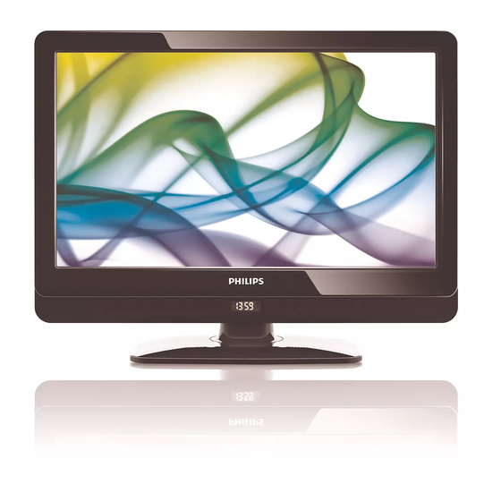
Colour Television
Contents
©
Copyright 2010 Koninklijke Philips Electronics N.V.
All rights reserved. No part of this publication may be reproduced, stored in a
retrieval system or transmitted, in any form or by any means, electronic, mechanical,
photocopying, or otherwise without the prior permission of Philips.
Published by MB/SaS/CC 1071 BU TV Consumer Care, the Netherlands
Page
Contents
2
11. Styling Sheets
2
P&S 22"
5
P&S 26"
9
P&S 32"
32
38
43
55
56
57
58
59
60
61
62
63
64
67
70
73
84
93
101
106
107
111
112
113
117
121
Chassis
Q552.1HE
Page
123
124
125
Subject to modification
EN 3122 785 19040
LA
19040_000_100914.eps
101110
Advertisement
Table of Contents


Need help?
Do you have a question about the P&S 22HFL4372D/10 and is the answer not in the manual?
Questions and answers