Advertisement
Quick Links
QQ
3 7 63 1515 0
SERVICE MANUAL
TE
L 13942296513
Contents
Safety precaution
Preventing static electricity
Location of main parts
Disassembly method
Adjustment method
www
.
http://www.xiaoyu163.com
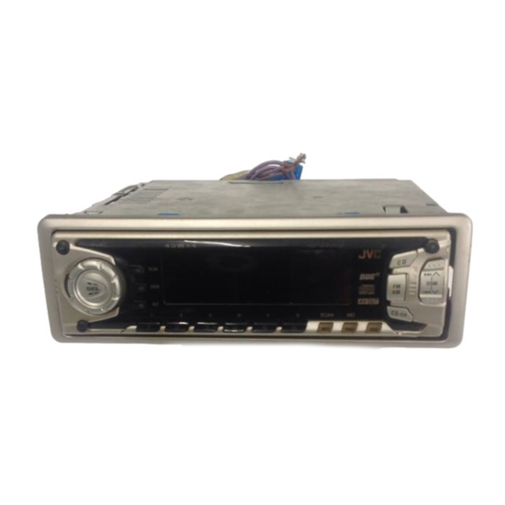
CD RECEIVER
KD-SX975 / KD-SX875
x
ao
y
i
COPYRIGHT
http://www.xiaoyu163.com
8
Q Q
3
6 7
1 3
1-2
Flow of functional
1-3
operation unit TOC read
1-4
Maintenance of laser pickup
1-5
Replacement of laser pickup
1-10
Discription of major ICs
u163
.
2001 VICTOR COMPANY OF JAPAN, LTD.
KD-SX975 / KD-SX875
2 9
9 4
2 8
1 5
0 5
8
2 9
9 4
Area Suffix
U ---- Other Areas
m
co
9 9
2 8
9 9
1-11
1-13
1-13
1-14
No.49620
Feb. 2001
Advertisement

Subscribe to Our Youtube Channel
Related Manuals for JVC KD-SX975


Summary of Contents for JVC KD-SX975
- Page 1 KD-SX975 / KD-SX875 3 7 63 1515 0 SERVICE MANUAL CD RECEIVER KD-SX975 / KD-SX875 L 13942296513 Area Suffix U ---- Other Areas Contents Safety precaution Flow of functional 1-11 Preventing static electricity operation unit TOC read Location of main parts...
- Page 2 KD-SX975 / KD-SX875 3 7 63 1515 0 Safety precaution Burrs formed during molding may be left over on some parts of the chassis. Therefore, pay attention to such burrs in the case of preforming repair of this system.
- Page 3 KD-SX975 / KD-SX875 3 7 63 1515 0 Preventing static electricity 1.Grounding to prevent damage by static electricity Electrostatic discharge (ESD), which occurs when static electricity stored in the body, fabric, etc. is discharged, can destroy the laser diode in the traverse unit (optical pickup). Take care to prevent this when performing repairs.
- Page 4 KD-SX975 / KD-SX875 3 7 63 1515 0 Location of main parts Control unit Display Front PCB Antenna Changer control jack connector Main unit 16 pin connector RCA jack Main board Power IC L 13942296513 Tuner pack Main board assembly...
- Page 5 KD-SX975 / KD-SX875 3 7 63 1515 0 Disassembly method Removing the front chassis (See Fig.1) 1. Remove two screws A and insert a screwdriver to the joints a on the side of the front chassis and two joints b on the right side, then detach the front chassis toward the front side.
- Page 6 KD-SX975 / KD-SX875 3 7 63 1515 0 Main amplifier board CN501 Removing the main amplifier board assembly (See Fig.4 and 5) Remove the front chassis. Remove the bottom cover. Remove the two screws C attaching the main amplifier board assembly on the bottom of the body.
- Page 7 KD-SX975 / KD-SX875 3 7 63 1515 0 Damper bracket <CD mechanism section> CD mechanism assembly Removing the CD mechanism control board (See Fig.1 and 2) Unsolder the part a and b on the CD mechanism control board. Remove the stator fixing the CD mechanism control board and the damper bracket (To remove the stator smoothly, pick up the center part).
- Page 8 KD-SX975 / KD-SX875 3 7 63 1515 0 Damper bracket assembly CD mechanism Removing the CD mechanism assembly (See Fig.1, 6 to 9) Prior to performing the following procedure, remove the CD mechanism control board and the front bracket (loading motor).
- Page 9 KD-SX975 / KD-SX875 3 7 63 1515 0 Removing the feed motor assembly FD screw Part i Feed motor assembly (See Fig.10) Prior to performing the following procedure, remove the CD mechanism control board, the front bracket Part j (loading motor) and the CD mechanism assembly.
- Page 10 Load impedance 4 (4 to 8 allowance) Line-out Level / Impedance: L 13942296513 KD-SX975 : 4.0 V 20 k load (full scale) KD-SX875 : 2.0 V 20 k load (full scale) How to connect the extension cable for adjusting EXTGS004-26P...
- Page 11 KD-SX975 / KD-SX875 3 7 63 1515 0 Flow of functional operation unit TOC read Power ON When the laser diode correctly Set Function CD When the pickup correctly moves emits to the inner area of the disc Microprocessor...
- Page 12 KD-SX975 / KD-SX875 3 7 63 1515 0 Feed section Is the voltage output at Is the wiring for IC521 Is 5V present at IC581 IC521 pin "53" 5V or 0V? (90)~(100) correct? pin "20"? Check CD 9V Check the vicinity of and 5V.
- Page 13 KD-SX975 / KD-SX875 3 7 63 1515 0 Maintenance of laser pickup (1) Cleaning the pick up lens Before you replace the pick up,please try to clean the lens with a alcohol soaked cotton swab. (2) Life of the laser diode When the life of the laser diode has expired, the following symptoms will appear.
-
Page 14: Block Diagram
KD-SX975 / KD-SX875 3 7 63 1515 0 Description of major ICs UPD178078GF-543 (IC701): SYSTEM CPU 1.Terminal layout 100 ~ 81 31 ~ 50 2.Block diagram TO0/VTR-CONT NC,JBUS-INT,SW1, 16-bit TIMER/ PORT 0 TI00/POWER REMOCON,PS1,PS2, EVENT COUNTER DETACH,NC TI01/CD-ON PORT 1... - Page 15 KD-SX975 / KD-SX875 3 7 63 1515 0 3.Pin function UPD178078GF(1/2) FUNCTION Symbol Non connection JBUS-INT JVC BUS COMMUNICATION LINE JBUS-SI JVC BUS COMMUNICATION LINE JBUS-SO JVC BUS COMMUNICATION LINE JBUS-SCK JVC BUS COMMUNICATION LINE Non connection Non connection...
- Page 16 KD-SX975 / KD-SX875 3 7 63 1515 0 UPD178078GF(2/2) FUNCTION Symbol CD MECHA SW REMOCON REMOCON INPUT VTR-LOGIC Non connection VTR-CONT Non connection POWER POWER CONT. CD-ON CD POWER CONT. MUTE MUTE CONT Non connection BUZZER BEEP FOR SW OPERATION...
- Page 17 KD-SX975 / KD-SX875 3 7 63 1515 0 BA3220FV-X(IC341/IC441) : Line Out Amp 1.Terminal layout 3220 2.Block diagram L 13942296513 OUTL OUTR RGND LGND REFR REFL FILTER u163 1-17 http://www.xiaoyu163.com...
- Page 18 KD-SX975 / KD-SX875 3 7 63 1515 0 BD3860K (IC301):E.Volume 1.Terminal layout 2.Bockdiagram GND FIL VCC SEL1 VIN1 LOUD1 HF1 LF1 DET1 VCA1 MIX1 BBOUT1 TIN1 TNF1 BNF1 BOUT1 POWER FADER SUPPLY MAIN INPUT OUTF1 CH1 FRONT TREBLE BASS...
- Page 19 KD-SX975 / KD-SX875 3 7 63 1515 0 HA13164(IC961):REGULATOR 1.Terminal layout 1 2 3 4 5 6 7 8 9 10 11 12 13 14 15 2.Block diagram 100u 0.1u BATT.DET OUT ANT OUT Surge Protector 0.1u EXT OUT...
- Page 20 KD-SX975 / KD-SX875 3 7 63 1515 0 HD74HC126FP-X (IC771) : Buffer 1.Terminal layout 3.Pin function Input Output Note: H : High L : Low X : H and L Z : H.L.X 2.Block diagram Output Input L 13942296513...
- Page 21 KD-SX975 / KD-SX875 3 7 63 1515 0 LC75873NW(IC601):LCD Driver 1.Pin layout 2.Block diagram VDD1 COMON SEGMENT DRIVER DRIVER VDD2 CLOCK SHIFT REGISTOR GENERATOR ADDRESS DETECTOR 3.Pin function Pin No. Pin name Description Segment outouts for displaying the display data...
-
Page 22: Table Of Contents
KD-SX975 / KD-SX875 3 7 63 1515 0 LA4743K(IC351):Power AMP 1.Block diagram 2200 F 0.022 F Vcc 1/2 Vcc 3/4 IN 1 OUT 1+ 0.22 F OUT 1- PWR GND1 Protective circuit OUT 2+ IN 2 OUT 2- 0.22 F... -
Page 23: Tab
KD-SX975 / KD-SX875 3 7 63 1515 0 2.Terminal layout 3.Pin function LA4743K Pin No. Symbol Function Header of IC Power GND OUTFR- Outpur(-) for front Rch STBY Stand by input Output (+) for front Rch OUTFR+ Power input... -
Page 24: Vcc
KD-SX975 / KD-SX875 3 7 63 1515 0 LA6567H-X(IC581):CD DRIVER 1.Pin layout & blockdiagram CH 3,4,5 Thermal shutdown VCC2 Power supply V05- V05+ S-GND V04+ VCONT V04- VIN4 V03+ VIN4G Signal system power supply V03- VCC-S L 13942296513 V02+... - Page 25 KD-SX975 / KD-SX875 3 7 63 1515 0 2. Pin function LA6567H-X(2/2) Pin no. Symbol Function VCC2 CH3,4,5 Power supply( It is short with VCC1,VCC-S) V05- Loading output(-) V05+ Loading terminal (+) V04+ CH4 Output terminal(+) V04- CH4 Output terminal(-)
- Page 26 KD-SX975 / KD-SX875 3 7 63 1515 0 TA2109F-X (IC501) : RF amp. 1. Pin layout 2. Block diagram 15k ohm 30k ohm 7.67k ohm 15k ohm 10k ohm SBAD 10k ohm 20uA 50k ohm 30k ohm 20pF 36pF...
- Page 27 KD-SX975 / KD-SX875 3 7 63 1515 0 TC9462F(IC521): 1.Pin layout & Block Diagram 50 V Servo 1bit 49 TRO control Clock 48 FOO generator TEZI 46 TEI 45 TSIN TEST1 44 SBAD Digital equalizer TEST2 43 FEI Address circuit...
- Page 28 KD-SX975 / KD-SX875 3 7 63 1515 0 TC9462F(2/3) Symbol Pin No. Function Remarks 2-state output 2/4 times speed at "VREF" voltage. HSSW (PVREF,HiZ) 1 bit DA converter zero detect flag output terminal. ZDET Phase difference signal output terminal of EFM 3-state output.
- Page 29 KD-SX975 / KD-SX875 3 7 63 1515 0 TC9462F(3/3) Symbol Pin No. Function Remarks Test input terminal, Normally, keep at "L" level Analog input. TESIN Test input/output terminal. Normally, keep at "L" level Analog input. TESIO1 Digital GND terminal...
-
Page 30: Vcc
KD-SX975 / KD-SX875 3 7 63 1515 0 NJM4565M-WE (IC111) : Ope. amp A OUTPUT A INPUT B OUTPUT A INPUT B INPUT B INPUT RPM6938-SV4(IC602) : Remote Censor L 13942296513 1.Block diagram Comp Rout Detector conversion trimming circuit... - Page 31 KD-SX975 / KD-SX875 3 7 63 1515 0 L 13942296513 u163 VICTOR COMPANY OF JAPAN, LIMITED MOBILE ELECTRONICS DIVISION PERSONAL & MOBILE NETWORK BUSINESS UNIT. 10-1,1Chome,Ohwatari-machi,Maebashi-city,Japan Printed in Japan (No.49620) 200102(V) http://www.xiaoyu163.com...
- Page 32 KD-SX975/KD-SX875 3 7 6 3 1 5 1 5 0 CD Mechanism ENC 1,2 SYSTEM VOLUME JOG CD PICKUP UNIT MECHA. SWITCH CONTROLLER EN601 SW1~4 IC701 uPD178078GF-543 REMOCON SPINDLE/FEED REMOTO CONTROL VOL CL MOTOR RECEIVER VOL DA IC680 SPINDLE...
- Page 33 KD-SX975 / KD-SX875 3 7 63 1515 0 < M E M O > L 13942296513 u163 http://www.xiaoyu163.com...
- Page 34 KD-SX975/KD-SX875 3 7 6 3 1 5 1 5 0 Standard schematic diagrams D951 R952 C952 0.047 1SS133 Receiver & system control section C951 1/50 IC351 LA4743K QAU0223-001 C351 2.2/50 33uH R351 R352 R324 R201 C203 1/50 C308 470P...
- Page 35 KD-SX975/KD-SX875 KD-SX975/KD-SX875 3 7 6 3 1 5 1 5 0 Mecha control circuit section R583 2.4K R582 8.2K R584 5.6K R212 R215 C583 0.47 8.2K( 1/10W) R211 C211 4.7/25 R213 47/6.3 R585 R-CH C213 120P LOADING- C113 LOADING+...
- Page 36 KD-SX975/KD-SX875 3 7 6 3 1 5 1 5 0 LCD driver & operation switch section QNZ0449-001 IC602 1 3 9 4 2 2 9 6 5 1 3 EN601 RPM6938-SV4 QSW0793-001 R657 REMOCON ACC5V R658 D657 ENC1 ENC2 UDZS5.6B-X...
- Page 37 KD-SX975/KD-SX875 KD-SX975/KD-SX875 3 7 6 3 1 5 1 5 0 Printed circuit boards Main board Main board (Forward side) (Reverse side) L961 C960 IC961 C371 J931 CN901 D962 D963 C372 R966 D960 J771 C965 C963 B962 C772 C981...
- Page 38 KD-SX975/KD-SX875 3 7 63 1515 0 Front board(Forward side) D601 IC602 D629 R606 S605 R607 S613 S614 S608 D628 R605 R604 D611 D613 D623 D622 S615 D624 D617 D614 S607 S604 S606 S609 D615 D612 LCD1 S603 D616 EN601...
- Page 39 KD-SX975/KD-SX875 3 7 63 1515 0 PARTS LIST [ KD-SX975 ] [ KD-SX875 ] * All printed circuit boards and its assemblies are not available as service parts. Area suffix U --------------------- Other Areas L 13942296513 - Contents -...
- Page 40 KD-SX975/KD-SX875 3 7 63 1515 0 Exploded view of general assembly and parts list Block No. L 13942296513 u163 http://www.xiaoyu163.com...
- Page 41 1 LOCK LEVER(O.L.) FSKW4013-002 T.SPRING 1 FOR OPEN LEVER VYTA526-002 BLIND GE10005-001A FRONT PANEL 1 KD-SX875 GE10005-002A FRONT PANEL 1 KD-SX975 GE30113-008A FINDER ASSY 1 KD-SX975 GE30113-009A FINDER LENS 1 KD-SX875 FSJK4009-001 REMOTE LENS 1 FOR REMOTE CON. GE20104-001B PRESET BUTTON...
- Page 42 RUBBER CONNECTO GE30114-001A LCD CASE FSJK3028-001 LCD LENS FSYH4061-001 LIGHTNG SHEET FSYH4036-052 SHEET FSKS3013-001 LENS CASE GE30155-002A NAME PLATE 1 KD-SX975 GE30154-002A NAME PLATE 1 KD-SX875 VMA4652-001SS EARTH PLATE FSKL4024-001 IC BRACKET GE40103-001A REG BRACKET GE40104-002B HEAT SINK FSKM3010-017 REAR BRACKET...
- Page 43 KD-SX975/KD-SX875 3 7 63 1515 0 CD mechanism assembly and parts list Block No. Grease TN-CCD1001Z-136J G-31SA G-31SA(Bottom side) RX-405 L 13942296513 u163 106 29 http://www.xiaoyu163.com...
- Page 44 KD-SX975/KD-SX875 3 7 63 1515 0 Parts list (CD mechanism) Block No. M2MM Item Parts number Parts name Q'ty Description Area 30310101T FRAME 30310103T DANPER PIN 30310107T UPPER PLATE 30310108T SEL STOP PLATE 30310142T SEL ARM (L)L 30310143T SEL ARM (R)L...
- Page 45 KD-SX975/KD-SX875 3 7 63 1515 0 Parts list (CD mechanism) Block No. M2MM Item Parts number Parts name Q'ty Description Area 64180403T DET SWITCH 2 ESE22MH3 68150232T CONNECTOR 1 TKC-W26X-C1 30311105T SOPPORT PLATE 30311138T GR MT BLK(N) 30311109T LDG GEAR (2)
- Page 46 KD-SX975/KD-SX875 3 7 63 1515 0 Electrical parts list (Main board) Block No. 01 Item Parts number Parts name Remarks Area Item Parts number Parts name Remarks Area BZ871 QAN0009-001Z BUZZER C 356 NCB31HK-223X C CAPACITOR NCB31EK-473X C CAPACITOR...
- Page 47 KD-SX975/KD-SX875 3 7 63 1515 0 Electrical parts list (Main board) Block No. 01 Item Parts number Parts name Remarks Area Item Parts number Parts name Remarks Area C 544 QERF0JM-107Z E CAPACITOR 100MF 20% 6.3V C 993 NCS31HJ-101X C.CAPACITOR...
- Page 48 KD-SX975/KD-SX875 3 7 63 1515 0 Electrical parts list (Main board) Block No. 01 Item Parts number Parts name Remarks Area Item Remarks Parts number Parts name Area L 551 QQL244J-4R7Z INDUCTOR R 302 NRSA63J-224X MG RESISTOR L 701...
- Page 49 KD-SX975/KD-SX875 3 7 63 1515 0 Electrical parts list (Main board) Block No. 01 Item Parts number Parts name Remarks Area Item Parts number Parts name Remarks Area R 475 NRSA02J-101X MG RESISTOR R 729 NRSA63J-473X MG RESISTOR R 476...
- Page 50 KD-SX975/KD-SX875 3 7 63 1515 0 Electrical parts list (Front board) Block No. 02 Item Parts number Parts name Remarks Area Item Parts number Parts name Remarks Area C 601 NBE20JM-475X TS E CAPACITOR R 611 NRSA63J-272X MG RESISTOR...
- Page 51 KD-SX975/KD-SX875 3 7 63 1515 0 < M E M O > L 13942296513 u163 3-13 http://www.xiaoyu163.com...
- Page 52 KD-SX975/KD-SX875 3 7 63 1515 0 Packing materials and accessories parts list Block No. Block No. L 13942296513 KIT:A4 u163 3-14 http://www.xiaoyu163.com...
- Page 53 POLY BAG 1 FOR INST. BOOK QPA00801205 POLY BAG QPA01003003 POLY BAG FSYH4036-068 SHEET QPC03004315P POLY BAG GE30123-020A CARTON 1 KD-SX975 GE30123-019A CARTON 1 KD-SX875 GE10008-001A EPS CUSHION Parts list (Accessories) Block No. M4MM Item Parts number Parts name Q'ty...
Need help?
Do you have a question about the KD-SX975 and is the answer not in the manual?
Questions and answers