
Subscribe to Our Youtube Channel
Related Manuals for Texas Instruments THS1030/31EVM


Summary of Contents for Texas Instruments THS1030/31EVM
- Page 1 THS1030/31EVM Evaluation Module for the THS1030/THS1031 10 Bit User’s Guide 2000 AAP Data Conversion SLAU040...
- Page 2 IMPORTANT NOTICE Texas Instruments and its subsidiaries (TI) reserve the right to make changes to their products or to discontinue any product or service without notice, and advise customers to obtain the latest version of relevant information to verify, before placing orders, that information being relied on is current and complete. All products are sold subject to the terms and conditions of sale supplied at the time of order acknowledgement, including those pertaining to warranty, patent infringement, and limitation of liability.
- Page 3 Preface Read This First About This Manual This manual describes the physical characteristics, functions, modes of op- eration, and configuration of the THS1030/31EVM evaluation module (EVM). How to Use This Manual Chapter 1 – Overview Chapter 2 – Physical Description Chapter 3 –...
-
Page 5: Table Of Contents
............THS1030/31EVM Operational Procedure . - Page 6 Running Title—Attribute Reference Figures 2–1 Silk Top ..............2–2 Silk Bottom .
- Page 7 Running Title—Attribute Reference Tables 2–1 Parts List ..............3–1 Output Connector J4 .
- Page 8 viii...
-
Page 9: Overview
Chapter 1 Overview This chapter gives a general overview of the THS1030/31EVM evaluation module (EVM), and describes some of the factors that must be considered in using this module. Topic Page Purpose ............ -
Page 10: Purpose
Purpose 1.1 Purpose The THS1030/31EVM evaluation module (EVM) provides a platform for evaluation of the THS1030 and THS1031 10-bit analog-to-digital converters (ADC) under various signal, reference, and supply conditions. Unless stated explicitly, the functionality described in this user’s guide applies to both THS1030 and THS1031 devices. -
Page 11: Ths1030/31Evm Operational Procedure
EVM components. 1.4 THS1030/31EVM Operational Procedure The THS1030/31EVM provides a flexible means of evaluating the THS1030 and THS1031 in a number of modes of operation. These are described more fully in chapter 4. The following basic setup procedure can be used as a board-... -
Page 13: Physical Description
Chapter 2 Physical Description This chapter describes the physical characteristics and PCB layout of the EVM, and lists the components used on the module. Topic Page PCB Layout ..........Parts List . -
Page 14: Pcb Layout
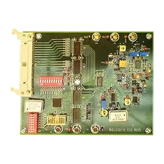
PCB Layout 2.1 PCB Layout The EVM is constructed on a 4-layer, 151-mm (5.94 ) 115-mm (4.54 ), 1.57-mm (0.062 ) thick PCB using FR-4 material. Figures 2–1 through 2–6 show the individual layers. Figure 2–1. Silk Top... -
Page 15: Silk Bottom
PCB Layout Figure 2–2. Silk Bottom Physical Description... - Page 16 PCB Layout Figure 2–3. Top...
- Page 17 PCB Layout Figure 2–4. Inner 1 Physical Description...
- Page 18 PCB Layout Figure 2–5. Inner 2...
- Page 19 PCB Layout Figure 2–6. Bottom Physical Description...
-
Page 20: Parts List
Parts LIst 2.2 Parts LIst Table 2–1 lists the parts used in constructing the EVM. Table 2–1. Parts List Reference Description Description Manufacturer Part Number LT1004-1.2 voltage reference LT1004CD-1-2 SN74AHC14D hex inverter SN74AHC14D U6 U8 U9 U10 SN74LVCC4245ADW bus transceiver SN74LVCC4245AD TLV2464CD quad opamp TLV2464CD... - Page 21 Parts LIst Table 2–1. Parts List (Continued) Reference Description Description Manufacturer Part Number R5, R6, R60, R61, R62, R63, 39R 0805 thick-film resistor 1% Multicomp CR10390FT R64, R65, R66, R67, R68, R69, R70, R71 R11, R12 100R 0805 thick-film resistor 1% Multicomp CR10101FT R53, R58...
- Page 22 2-10...
-
Page 23: Circuit Description
Chapter 3 Circuit Description This chapter contains the EVM schematic diagram and discusses the various functions on the EVM. Topic Page Schematic Diagram ......... . . Circuit Function . -
Page 24: Schematic Diagram
Schematic Diagram 3.1 Schematic Diagram Figures 3–1 through 3–5 show the schematic diagram for the EVM. The follow- ing paragraphs describe the EVM circuits. Figure 3–1. EVM Schematic Diagram DIPS LOGIC DAC[9:0] DAC[9:0] PGA[2:0] PGA[2:0] THS1031 POWERDOWN POWERDOWN IECLAMP IECLAMP POWER_&_REF IO[9:0] IO[9:0]... -
Page 25: Evm Schematic Diagram - Dips
Schematic Diagram Figure 3–2. EVM Schematic Diagram – DIPS Circuit Description... -
Page 26: Evm Schematic Diagram - Logic
Schematic Diagram Figure 3–3. EVM Schematic Diagram – LOGIC... -
Page 27: Evm Schematic Diagram - Ths1031
Schematic Diagram Figure 3–4. EVM Schematic Diagram – THS1031 Circuit Description... -
Page 28: Circuit Function
Circuit Function Figure 3–5. EVM Schematic Diagram – POWER_&_REF +3TO5VA +3TO5VA +3TO5VA +3TO5VA TP23 4 U7.B 330R U7.A 4MM Sockets TP15 +5 V TP24 10 k – 2N3906 820R – TLV2464 TLV2464 EXT_T 10 µ F 1 k5 0.1 µ F 0.1 µ... -
Page 29: Clock Options
Circuit Function 74AHC14 hex inverter IC (U4), then it should be ac-coupled through C24, with its dc level trimmed using potentiometer P1 if necessary. 3.2.2 Clock Options The EVM provides flexibility as to the source of the ADC conversion clock: this can come from an external source as described above, or from a crystal-oscil- lator module when U3 is populated with a standard DIL14 HCMOS. - Page 30 Circuit Function Table 3–1. Output Connector J4 J4 Pin Output Function J4 Pin Output Function I/O9 DATA I/O8 DATA I/O7 DATA I/O6 DATA I/O5 DATA I/O4 DATA I/O3 DATA I/O2 DATA I/O1 DATA I/O0 DATA 3.2.6 THS1031 Register Write The THS1031 has a number of registers that can be written to put the device into various modes of operation (see data sheet).
-
Page 31: Modes Of Operation
Chapter 4 Modes of Operation The EVM can be easily configured, via jumper connections, to operate the THS1030/31 in various modes of operation. Figures 4–1 to 4–7 depict various modes of operation, with Tables 4–1 and 4–2 listing the corresponding jumper settings. -
Page 32: Common Mode Input Vref/2 - 1Vp-P Input Span (Top/Bottom Mode)
Figure 4–1. Common Mode Input VREF/2 – 1Vp-p Input Span (top/bottom mode) THS1030/31 REFTS REFBS MODE AVDD REFTF 0.1 µF – 10 µF 0.1 µF VREF 0.1 µF REFSENSE REFBF Figure 4–2. Common Mode Input VREF/2 – 2Vp-p Input Span (top/bottom mode) THS1030/31 REFTS REFBS... -
Page 33: External Common Mode Input - 1Vp-P Input Span (Center Span Mode)
Figure 4–3. External Common Mode Input – 1Vp-p Input Span (center span mode) THS1030/31 REFTS 1.5 V REFBS MODE AVDD/2 REFTF 0.1 µF – 10 µF 0.1 µF VREF 0.1 µF REFBF REFSENSE Figure 4–4. External Common Mode Input – 2Vp-p Input Span (center span mode) 2.5 V THS1030/31 0.5 V... -
Page 34: Differential Input - 1Vp-P Input Span (Differential Input Mode)
Figure 4–5. Differential Input – 1Vp-p Input Span (differential input mode) THS1030/31 COM = AVDD/2 REFTS REFBS MODE AVDD/2 REFTF 0.1 µF – 10 µF 0.1 µF VREF 0.1 µF REFBF REFSENSE Figure 4–6. Differential Input – 2Vp-p Input Span (differential input mode) THS1030/31 COM = AVDD/2 REFTS... -
Page 35: External Reference - Input Span And Bias Set By On Board Reference Circuit
Figure 4–7. External Reference – Input Span and Bias Set by on Board Reference Circuit (potentiometer P2 sets EXT_T, potentiometer P3 sets EXT_B) THS1030/31 REFBF REFTF MODE REFTF EXT_T 0.1 µF – 10 µF 0.1 µF VREF EXT_B REFBF 0.1 µF REFSENSE AVDD Modes of Operation... -
Page 36: Bottom
Table 4–1. Board Jumper Settings for Various Modes of Operation Mode : Top/Bottom Top/Bottom Cent. Span Cent. Span Differential Differential Ext. Ref. (1V) (2V) (1V) (2V) (1V) (2V) Reference: Ext. Only Refbs/bf – – POT P3 POT P3 – – POT P3 Refts/tf –... - Page 37 LINK 9 LINK 10 LINK 11 LINK 13 LINK 14 LINK 15 LINK 16 Figure 4–1 Figure 4–2 Figure 4–3 Figure 4–4 Figure 4–5 Figure 4–6 Figure 4–7 Table 4–2. Jumper Settings for Clock Options Clock Onboard External AC External DC Options Oscillator coupled Via J2...
- Page 38 Modes of Operation...
- Page 39 Mouser Electronics Authorized Distributor Click to View Pricing, Inventory, Delivery & Lifecycle Information: Texas Instruments THS1031EVM THS1030EVM...
Need help?
Do you have a question about the THS1030/31EVM and is the answer not in the manual?
Questions and answers