Table of Contents
Advertisement
Quick Links
Advertisement
Table of Contents

Related Manuals for Asus Aaeon PCM-CFS


Summary of Contents for Asus Aaeon PCM-CFS
- Page 1 PCM-CFS 5.25” Compact Board User’s Manual 11 Last Updated: April 15, 2021...
- Page 2 Copyright Notice This document is copyrighted, 2021. All rights are reserved. The original manufacturer reserves the right to make improvements to the products described in this manual at any time without notice. No part of this manual may be reproduced, copied, translated, or transmitted in any form or by any means without the prior written permission of the original manufacturer.
- Page 3 Acknowledgement All other products’ name or trademarks are properties of their respective owners. Microsoft Windows is a registered trademark of Microsoft Corp. ⚫ Intel® and Celeron® are registered trademarks of Intel Corporation ⚫ Core™ is a trademark of Intel Corporation ⚫...
- Page 4 Packing List Before setting up your product, please make sure the following items have been shipped: Item Quantity PCM-CFS Jumper Cap (9657666600) Backplate for cooler (M09KBS9000) If any of these items are missing or damaged, please contact your distributor or sales representative immediately.
- Page 5 About this Document This User’s Manual contains all the essential information, such as detailed descriptions and explanations on the product’s hardware and software features (if any), its specifications, dimensions, jumper/connector settings/definitions, and driver installation instructions (if any), to facilitate users in setting up their product. Users may refer to the product page at AAEON.com for the latest version of this document.
- Page 6 Safety Precautions Please read the following safety instructions carefully. It is advised that you keep this manual for future references All cautions and warnings on the device should be noted. Make sure the power source matches the power rating of the device. Position the power cord so that people cannot step on it.
- Page 7 If any of the following situations arises, please the contact our service personnel: Damaged power cord or plug Liquid intrusion to the device iii. Exposure to moisture Device is not working as expected or in a manner as described in this manual The device is dropped or damaged Any obvious signs of damage displayed on the device...
- Page 8 FCC Statement This device complies with Part 15 FCC Rules. Operation is subject to the following two conditions: (1) this device may not cause harmful interference, and (2) this device must accept any interference received including interference that may cause undesired operation.
- Page 9 China RoHS Requirements (CN) 产品中有毒有害物质或元素名称及含量 AAEON Main Board/ Daughter Board/ Backplane 有毒有害物质或元素 部件名称 铅 汞 镉 六价铬 多溴联苯 多溴二苯醚 (Pb) (Hg) (Cd) (Cr(VI)) (PBB) (PBDE) 印刷电路板 ○ ○ ○ ○ ○ ○ 及其电子组件 外部信号 ○ ○ ○ ○ ○ ○ 连接器及线材...
- Page 10 China RoHS Requirement (EN) Poisonous or Hazardous Substances or Elements in Products AAEON Main Board/ Daughter Board/ Backplane Poisonous or Hazardous Substances or Elements Hexavalent Polybrominated Polybrominated Component Lead Mercury Cadmium Chromium Biphenyls Diphenyl Ethers (Pb) (Hg) (Cd) (Cr(VI)) (PBB) (PBDE) PCB &...
-
Page 11: Table Of Contents
Table of Contents Chapter 1 - Product Specifications..................1 Specifications ......................2 Chapter 2 – Hardware Information ..................4 Dimensions ....................... 5 Jumpers and Connectors ..................6 List of Jumpers ......................8 2.3.1 Touch Screen 4/5-Wire Mode Selection (JP1) ........8 2.3.2 COM2 Pin 9 Function Selection .............. - Page 12 2.4.12 COM Port 1, 3, 4, 5 (CN14/ CN17/ CN18/ CN19) ......... 26 2.4.13 COM Port 2, Port 6 (CN15/CN20) ............27 2.4.14 LPC Port (CN21)..................30 2.4.15 PCI Slot (CN22)................... 30 2.4.16 COM Port 7, 8, 9, 10 (CN23/ CN24/ CN28/ CN29) ......31 2.4.17 PCI-Express [x16] Slot (CN25) ..............
- Page 13 AMI BIOS Setup ...................... 51 Main.......................... 52 Advanced ........................ 53 3.4.1 Trusted Computing ..................54 3.4.2 CPU Configuration ..................56 3.4.3 SATA Configuration ................... 58 3.4.4 Hardware Monitor ..................60 3.4.4.1 Smart Fan Mode Configuration ............61 3.4.5 SIO Configuration ..................63 3.4.5.1 Serial Port 1 Configuration ..............
- Page 14 3.5.2 PCH-IO Configuration ................84 Security ........................85 3.6.1 Secure Boot ....................86 3.6.1.1 Key Management ................87 Boot .......................... 89 3.7.1 BBS Priorities ....................90 Save & Exit ....................... 91 Chapter 4 – Drivers Installation .................... 92 Driver Download/Installation ................93 Appendix A - Watchdog Timer Programming ..............
-
Page 15: Chapter 1 - Product Specifications
Chapter 1 Chapter 1 - Product Specifications... -
Page 16: Specifications
Specifications System Form Factor 5.25” Compact Board 8th/9th Generation Intel® Core™ i7/i5/i3 and Celeron® Socket Type (up to 65W) CPU Frequency Up to 5.0GHz Chipset Intel® Q370 (TDP: 6W) Memory Type SODIMM DDR4 Memory Slot x 2 Max. Memory Capacity Up to 32GB BIOS UEFI only... - Page 17 Display Backlight inverter supply 18/24bit (2CH) Ethernet Intel® GbE i219 x 1 Intel® GbE i211 x 1 Audio ALC269 (With Amplifier) USB Port USB 3.2 Gen 1 x 4 (headers) USB 2.0 x 4 (headers) Serial Port RS232 x 8 (headers) RS232/422/485 x 2 (headers) Parallel Port —...
-
Page 18: Chapter 2 - Hardware Information
Chapter 2 Chapter 2 – Hardware Information... -
Page 19: Dimensions
Dimensions Chapter 2 – Hardware Information... -
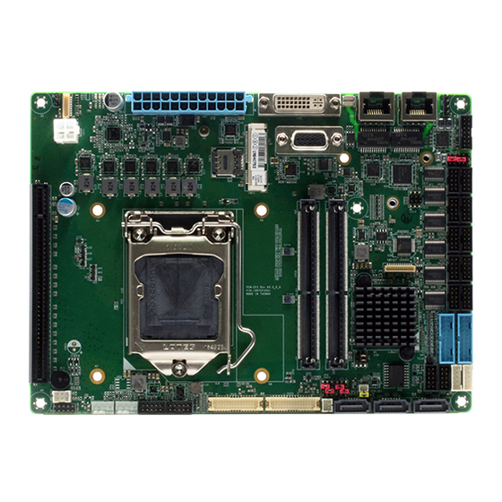
Page 20: Jumpers And Connectors
Jumpers and Connectors Processor Side Chapter 2 – Hardware Information... - Page 21 Solder Side Chapter 2 – Hardware Information...
-
Page 22: List Of Jumpers
List of Jumpers Please refer to the table below for all of the board’s jumpers that you can configure for your application Label Function Touch Screen 4/5-Wire Mode Selection COM2 Pin 9 Function Selection COM6 Pin 9 Function Selection Auto Power Button Enable/ Disable Selection LVDS Port 1 and Port 2 Backlight Brightness Control Mode Selection LVDS Port 1 Operating VDD Selection, Backlight Inverter VCC Selection LVDS Port 2 Operating VDD Selection, Backlight Inverter VCC Selection... -
Page 23: Com6 Pin 9 Function Selection (Jp3)
2.3.3 COM6 Pin 9 Function Selection (JP3) +12V Ring (Default) 2.3.4 Auto Power Button Enable/Disable Selection (JP4) Disable/ATX (Default) Enable/AT Note: When “Disable” is selected (JP4 pins 1-2), the power button is required to power on the system. Front Panel (JP9) needs to be set to pins 1-2 to use power button. 2.3.5 LVDS Port Backlight Brightness Control Mode Selection (JP5) Port 1... -
Page 24: Lvds Operating Vdd/Backlight Inverter Selection (Jp6/Jp7)
2.3.6 LVDS Operating VDD/Backlight Inverter Selection (JP6/JP7) Operating VDD Selection +3.3V (Default) Backlight Inverter VCC Selection +12V +5V (Default) Note: To avoid damage to components, do not use any other configuration for JP6 or JP7 than those shown above! 2.3.7 Clear CMOS Jumper (JP8) Disable/ATX (Default) Enable/AT... -
Page 25: Front Panel Connector (Jp9)
2.3.8 Front Panel Connector (JP9) Pin Name Pin Name PWR_BTN- PWR_BTN+ HDD_LED- HDD_LED+ SPEAKER- SPEAKER+ PWR_LED- PWR_LED+ H/W RESET- H/W RESET+ Chapter 2 – Hardware Information... -
Page 26: List Of Connectors
List of Connectors Please refer to the table below for all of the board’s connectors that you can configure for your application Label Function ATX Power Connector Stereo Audio Output Connector DVI Connector Touch Screen Connector RJ-45 Ethernet 1 Connector RJ-45 Ethernet 2 Connector Ethernet 1 Connector (Optional) Ethernet 2 Connector (Optional) - Page 27 Label Function CN25 PCI Express [x16] Slot CN26 DDR4 SO-DIMM Channel B Slot CN27 DDR4 SO-DIMM Channel A Slot CN28 COM Port 9 CN29 COM Port 10 CN30 USB 3.0 Ports 2 and 3 CN31 USB 3.0 Ports 0 and 1 CN32 LVDS Port 1 Inverter/ Backlight Connector CN33...
-
Page 28: Atx Power Connector (Cn1)
2.4.1 ATX Power Connector (CN1) Pin Name Signal Type Signal level +3.3V +3.3V +3.3V +3.3V PWR_OK +5VSB +12V +12V +12V +12V +3.3V +3.3V +3.3V +3.3V -12V -12V PS_ON# Chapter 2 – Hardware Information... -
Page 29: Stereo Audio Output Connector (Cn2)
Pin Name Signal Type Signal level 2.4.2 Stereo Audio Output Connector (CN2) Pin Name Signal Type Signal level SPK_OUT_R+ SPK_OUT_R- SPK_OUT_L+ SPK_OUT_L- Chapter 2 – Hardware Information... -
Page 30: Dvi Connector (Cn3)
2.4.3 DVI Connector (CN3) Pin Name Signal Type Signal level TMDS_DAT2- DIFF TMDS_DAT2+ DIFF DVI_DDC_CLK DVI_DDC_DATA VSYNC TMDS_DAT1- DIFF TMDS_DAT1+ DIFF HPLG_DETECT TMDS_DAT0- DIFF TMDS_DAT0+ DIFF Chapter 2 – Hardware Information... -
Page 31: Touch Screen Connector (Cn4)
Pin Name Signal Type Signal level TMDS_CLK+ DIFF TMDS_CLK- DIFF GREEN BLUE HSYNC 2.4.4 Touch Screen Connector (CN4) Note: Touch mode is set by Touch Screen Mode Selection JP1 8-Wire Mode Pin Name Signal Type Signal level TOP EXCITE BOTTOM EXCITE LEFT EXCITE RIGHT EXCITE Chapter 2 –... - Page 32 8-Wire Mode Pin Name Signal Type Signal level TOP SENSE BOTTOM SENSE LEFT SENSE RIGHT SENSE 4-Wire Mode Pin Name Signal Type Signal level BOTTOM LEFT RIGHT Chapter 2 – Hardware Information...
-
Page 33: Ethernet 1/ 2 Connector (Cn5/Cn6)
5-Wire Mode Pin Name Signal Type Signal level UL(Y) UR(H) LL(L) LR(X) SENSE(S) 2.4.5 RJ-45 Ethernet 1/ 2 Connector (CN5/CN6) Pin Name Signal Type Signal level MDI0+ DIFF MDI0- DIFF MDI1+ DIFF Chapter 2 – Hardware Information... -
Page 34: Ethernet 1/ 2 Connector (Optional) (Cn7/Cn8)
Pin Name Signal Type Signal level MDI2+ DIFF MDI2- DIFF MDI1- DIFF MDI3+ DIFF MDI3- DIFF 2.4.6 Ethernet 1/ 2 Connector (Optional) (CN7/CN8) Pin Name Signal Type Signal level MDI0+ DIFF MDI0- DIFF MDI1+ DIFF MDI1- DIFF MDI2+ DIFF MDI2- DIFF MDI3+ DIFF... -
Page 35: Audio In/Out And Mic Connector
2.4.7 Audio In/Out and MIC Connector MIC_R MIC_L GND_AUDIO LINE_L_IN LINE_R_IN GND_AUDIO RIGHT_OUT LEFT_OUT GND_AUDIO GND_AUDIO Pin Name Signal Type Signal level MIC_R MIC_L GND_AUDIO LINE_L_IN LINE_R_IN GND_AUDIO LEFT_OUT RIGHT_OUT GND_AUDIO GND_AUDIO Chapter 2 – Hardware Information... -
Page 36: D-Sub Crt Connector (Cn10)
2.4.8 D-SUB CRT Connector (CN10) Pin Name Signal Type Signal level GREEN BLUE RED_GND_RTN GREEN_GND_RTN BLUE_GND_RTN DDC_DATA HSYNC VSYNC DDC_CLK Chapter 2 – Hardware Information... -
Page 37: Mini-Card Slot (Half-Size) (Cn11)
2.4.9 Mini-Card Slot (Half-Size) (CN11) Pin Name Signal Type Signal level PCIE_WAKE# +3.3VSB +3.3V +1.5V +1.5V PCIE_CLK_REQ# UIM_PWR UIM_DATA PCIE_REF_CLK- DIFF UIM_CLK PCIE_REF_CLK+ DIFF UIM_RST UIM_VPP W_DISABLE# +3.3V PCIE_RST# +3.3V PCIE_RX- DIFF +3.3VSB +3.3V Chapter 2 – Hardware Information... - Page 38 Pin Name Signal Type Signal level PCIE_RX+ DIFF +1.5V +1.5V SMB_CLK +3.3V PCIE_TX- DIFF SMB_DATA +3.3V PCIE_TX+ DIFF USB_D- DIFF USB_D+ DIFF +3.3VSB +3.3V +3.3VSB +3.3V +1.5V +1.5V Chapter 2 – Hardware Information...
-
Page 39: Ethernet Led Indicator (Cn12/Cn16)
Pin Name Signal Type Signal level +3.3VSB +3.3V 2.4.10 Ethernet LED Indicator (CN12/CN16) Pin Name Signal Type Signal level ACT_LED+ ACT_LED- 100_LED+ 100_LED- 1000_LED+ 1000_LED- 2.4.11 Nano-SIM Card Connector (CN13) Pin Name Signal Type Signal level UIM_PWR UIM_RST UIM_CLK UIM_VPP UIM_DATA Chapter 2 –... -
Page 40: Com Port 1, 3, 4, 5 (Cn14/ Cn17/ Cn18/ Cn19)
2.4.12 COM Port 1, 3, 4, 5 (CN14/ CN17/ CN18/ CN19) Pin Name Signal Type Signal level ±9V ±9V ±9V Chapter 2 – Hardware Information... -
Page 41: Com Port 2, Port 6 (Cn15/Cn20)
2.4.13 COM Port 2, Port 6 (CN15/CN20) Note: COM Port 2 and Port 6 Mode (RS-232/422/485) can be set by BIOS (see Chatper 3). Default setting is RS-232. Pin 9 function can be set by COM2 Pin 9 Function Jumper (JP2) for Port 2 and COM6 Pin 9 Function Jumper (JP3) for Port 6. - Page 42 RS-485 Mode Pin Name Signal Type Signal level RS485_D- ±5V RS485_D+ ±5V NC/+5V/+12V +5V/+12V Chapter 2 – Hardware Information...
- Page 43 RS-422 Mode Pin Name Signal Type Signal level RS422_TX- ±5V RS422_TX+ ±5V RS422_RX+ RS422_RX- NC/+5V/+12V +5V/+12V Chapter 2 – Hardware Information...
-
Page 44: Lpc Port (Cn21)
2.4.14 LPC Port (CN21) Pin Name Signal Type Signal level LAD0 +3.3V LAD1 +3.3V LAD2 +3.3V LAD3 +3.3V +3.3V +3.3V LFRAME# LRESET# +3.3V LCLK SMB_DATA +3.3V SMB_CLK +3.3V SERIRQ +3.3V 2.4.15 PCI Slot (CN22) Standard specification. Chapter 2 – Hardware Information... -
Page 45: Com Port 7, 8, 9, 10 (Cn23/ Cn24/ Cn28/ Cn29)
2.4.16 COM Port 7, 8, 9, 10 (CN23/ CN24/ CN28/ CN29) Pin Name Signal Type Signal level ±9V ±9V ±9V 2.4.17 PCI-Express [x16] Slot (CN25) Standard specification. 2.4.18 DDR SO-DIMM Slot (CN26/27) Standard specification. Chapter 2 – Hardware Information... -
Page 46: Usb 3.0 Ports 2 And 3 (Cn30)
2.4.19 USB 3.0 Ports 2 and 3 (CN30) PIN1 PIN19 PIN11 PIN10 Pin Name Signal Type Signal level +5VSB USB2_SSRX− DIFF USB2_SSRX+ DIFF USB2_SSTX− DIFF USB2_SSTX+ DIFF USB2_D- DIFF USB2_D+ DIFF USB3_D+ DIFF USB3_D- DIFF USB3_SSTX+ DIFF USB3_SSTX− DIFF USB3_SSRX+ DIFF USB3_SSRX−... -
Page 47: Usb 3.0 Ports 0 And 1 (Cn31)
2.4.20 USB 3.0 Ports 0 and 1 (CN31) PIN1 PIN19 PIN11 PIN10 Pin Name Signal Type Signal level +5VSB USB0_SSRX− DIFF USB0_SSRX+ DIFF USB0_SSTX− DIFF USB0_SSTX+ DIFF USB0_D- DIFF USB0_D+ DIFF USB1_D+ DIFF USB1_D- DIFF USB1_SSTX+ DIFF USB1_SSTX− DIFF USB1_SSRX+ DIFF USB1_SSRX−... -
Page 48: Lvds Port Inverter/Backlight Connector (Cn32/33)
2.4.21 LVDS Port Inverter/Backlight Connector (CN32/33) BLK_PWR BKL_CONTROL BKL_ENABLE Pin Name Signal Type Signal level BKL_PWR +5V/+12V BKL_CONTROL BKL_ENABLE Note: LVDS1 BKL_PWR can be set by JP6. BKL_CTL can be set by JP5 (Pins 1/3/5). Note: LVDS2 BKL_PWR can be set by JP7. BKL_CTL can be set by JP5 (Pins 2/4/6). 2.4.22 USB 2.0 Ports 4 and 5 (CN34) USB4_D-... -
Page 49: Usb 2.0 Ports 6 And 7 (Cn35)
Pin Name Signal Type Signal level USB5_D- DIFF +5VSB 2.4.23 USB 2.0 Ports 6 and 7 (CN35) USB4_D- USB4_D+ USB5_D+ USB5_D- Pin Name Signal Type Signal level +5VSB USB6_D- DIFF USB6_D+ DIFF USB7_D+ DIFF USB7_D- DIFF +5VSB 2.4.24 Battery Connector (CN36) Pin Name Signal Type Signal level... -
Page 50: Ps/2 Keyboard/Mouse Combo Port
2.4.25 PS/2 Keyboard/Mouse Combo Port Pin Name Signal Type Signal level KB_ DATA KB_CLK +5VSB MS_DATA MS_CLK 2.4.26 LVDS Port 1 (CN38) Note: LCD_PWR can be set by Jumper JP6 Pin Name Signal Type Signal level BKL_ENABLE BKL_CONTROL LCD_PWR +3.3V/+5V Chapter 2 –... - Page 51 Pin Name Signal Type Signal level LVDS_A_CLK- DIFF LVDS_A_CLK+ DIFF LCD_PWR +3.3V/+5V LVDS_DA0- DIFF LVDS_DA0+ DIFF LVDS_DA1- DIFF LVDS_DA1+ DIFF LVDS_DA2- DIFF LVDS_DA2+ DIFF LVDS_DA3- DIFF LVDS_DA3+ DIFF DDC_DATA +3.3V DDC_CLK +3.3V LVDS_DB0- DIFF LVDS_DB0+ DIFF LVDS_DB1- DIFF LVDS_DB1+ DIFF LVDS_DB2- DIFF LVDS_DB2+...
-
Page 52: Lvds Port 2 (Cn39)
2.4.27 LVDS Port 2 (CN39) Note: LCD_PWR can be set by Jumper JP6 Pin Name Signal Type Signal level BKL_ENABLE BKL_CONTROL LCD_PWR +3.3V/+5V LVDS_A_CLK- DIFF LVDS_A_CLK+ DIFF LCD_PWR +3.3V/+5V LVDS_DA0- DIFF LVDS_DA0+ DIFF LVDS_DA1- DIFF LVDS_DA1+ DIFF LVDS_DA2- DIFF LVDS_DA2+ DIFF LVDS_DA3- DIFF... -
Page 53: +5V Output For Sata Hdd
Pin Name Signal Type Signal level DDC_DATA +3.3V DDC_CLK +3.3V LVDS_DB0- DIFF LVDS_DB0+ DIFF LVDS_DB1- DIFF LVDS_DB1+ DIFF LVDS_DB2- DIFF LVDS_DB2+ DIFF LVDS_DB3- DIFF LVDS_DB3+ DIFF LCD_PWR +3.3V/+5V LVDS_B_CLK- DIFF LVDS_B_CLK+ DIFF 2.4.28 +5V Output for SATA HDD Pin Name Signal Type Signal level Chapter 2 –... -
Page 54: Sata Port Connector (Cn41/ Cn42/ Cn43)
2.4.29 SATA Port Connector (CN41/ CN42/ CN43) Pin Name Signal Type Signal level SATA_TX+ DIFF SATA_TX- DIFF SATA_RX- DIFF SATA_RX+ DIFF 2.4.30 CPU Fan Connector (CN44) FAN_TAC FAN_POWER FAN_CTL Pin Name Signal Type Signal level FAN_POWER +12V FAN_TAC FAN_CTL +3.3V Chapter 2 –... -
Page 55: System Fan Connector (Cn45)
2.4.31 System Fan Connector (CN45) Pin Name Signal Type Signal level FAN_POWER +12V FAN_TAC FAN_CTL +3.3V 2.4.32 Digital IO Port 1/Port 2 Connector (CN46/ CN50) Pin Name Signal Type Signal level DIO0 DIO1 DIO2 DIO3 DIO4 DIO5 DIO6 DIO7 Chapter 2 – Hardware Information... -
Page 56: 2280 B-Key Slot (Cn47)
2.4.33 M.2 2280 B-Key Slot (CN47) Pin Name Signal Type Signal level CONFIG3 +3.3V +3.3V +3.3V +3.3V USB_D+ DIFF W_DISABLE# USB_D- DIFF SATA_LED +3.3V CONFIG0 PCIE_RX- DIFF PCIE_RX+ DIFF Chapter 2 – Hardware Information... - Page 57 Pin Name Signal Type Signal level PCIE_TX- DIFF PCIE_TX+ DIFF SATA_RX+ DIFF SATA_RX- DIFF SATA_TX- DIFF SATA_TX+ DIFF PERST# +3.3V PCIE_CLK_REQ# +3.3V PCIE_CLK- DIFF PCIE_WAKE +3.3V PCIE_CLK+ DIFF Chapter 2 – Hardware Information...
-
Page 58: 2280 M-Key Slot (Cn48)
Pin Name Signal Type Signal level CONFIG1 +3.3V +3.3V +3.3V +3.3V +3.3V +3.3V CONFIG2 2.4.34 M.2 2280 M-Key Slot (CN48) Pin Name Signal Type Signal level +3.3V +3.3V +3.3V +3.3V PCIE3_RX- DIFF PCIE3_RX+ DIFF Chapter 2 – Hardware Information... - Page 59 Pin Name Signal Type Signal level SATA_LED +3.3V PCIE3_TX- +3.3V +3.3V PCIE3_TX+ +3.3V +3.3V +3.3V +3.3V PCIE2_RX- DIFF +3.3V +3.3V PCIE2_RX+ DIFF PCIE2_TX- DIFF PCIE2_TX+ DIFF PCIE1_RX- DIFF PCIE1_RX+ DIFF PCIE1_TX- DIFF Chapter 2 – Hardware Information...
- Page 60 Pin Name Signal Type Signal level PCIE1_TX+ DIFF DECSLP PCIE0_RX- DIFF PCIE0_RX+ DIFF PCIE0_TX- DIFF PCIE0_TX+ DIFF PERST# PCIE_CLK_REQ# PCIE_CLK- DIFF PCIE_WAKE PCIE_CLK+ DIFF +3.3V +3.3V Chapter 2 – Hardware Information...
-
Page 61: Spi Flash Programming Port (Cn49)
Pin Name Signal Type Signal level +3.3V +3.3V +3.3V +3.3V 2.4.35 SPI Flash Programming Port (CN49) P IN 1 P IN 2 P IN 3 P IN 4 P IN 5 P IN 6 P IN 7 Pin Name Signal Type Signal level SPI_MISO SPI_CLK... -
Page 62: Block Diagram
Block Diagram Chapter 2 – Hardware Information... -
Page 63: Chapter 3 - Ami Bios Setup
Chapter 3 Chapter 3 - AMI BIOS Setup... -
Page 64: System Test And Initialization
System Test and Initialization The system uses certain routines to perform testing and initialization during the boot up sequence. If an error, fatal or non-fatal, is encountered, the system will output a few short beeps or an error message. The board can usually continue the boot up sequence with non-fatal errors. -
Page 65: Ami Bios Setup
AMI BIOS Setup The AMI BIOS ROM has a pre-installed Setup program that allows users to modify basic system configurations, which is stored in the battery-backed CMOS RAM and BIOS NVRAM so that the information is retained when the power is turned off. To enter BIOS Setup, press <Del>... -
Page 66: Main
Main Chapter 3 – AMI BIOS Setup... -
Page 67: Advanced
Advanced Chapter 3 – AMI BIOS Setup... -
Page 68: Trusted Computing
3.4.1 Trusted Computing Options Summary Security Device Support Disable Enable Optimal Default, Failsafe Default Enables or Disables BIOS support for security device. O.S. will not show Security Device. TCG EFI protocol and INT1A interface will not be available. SHA-1 PCR Bank Disable Enable Optimal Default, Failsafe Default... - Page 69 Options Summary Platform Hierarchy Disabled Enabled Optimal Default, Failsafe Default Enable or disable Platform Hierarchy Storage Hierarchy Disabled Enabled Optimal Default, Failsafe Default Enable or Disable Storage Hierarchy Endorsement Hierarchy Disabled Enabled Optimal Default, Failsafe Default Enable or Disable Endorsement Hierarchy TPM2.0 UEFI Spec Version TCG_1_2 TCG_2 Optimal Default, Failsafe Default...
-
Page 70: Cpu Configuration
3.4.2 CPU Configuration Options Summary Hyper-Threading Disabled Enabled Optimal Default, Failsafe Default Enabled or Disabled Hyper-Threading Technology Active Processor Cores Optimal Default, Failsafe Default Number of cores to enable in each processor package. Intel (VMX) Virtualization Disabled Technology Enabled Optimal Default, Failsafe Default When enabled, a VMM can utilize the additional hardware capabilities provided by Vanderpool Technology. - Page 71 Options Summary Intel(R) SpeedStep(tm) Disabled Enabled Optimal Default, Failsafe Default Allows more than two frequency ranges to be supported. Turbo Mode Disabled Enabled Optimal Default, Failsafe Default Enable/Disable processor Turbo Mode (requires Intel Speed Step or Intel Speed Shift to be available and enabled).
-
Page 72: Sata Configuration
3.4.3 SATA Configuration Options Summary SATA Controller(s) Disabled Enabled Optimal Default, Failsafe Default Enable/Disable SATA Device. SATA Mode Selection AHCI Optimal Default, Failsafe Default Intel RST Premium With Intel Optane System Acceleration Determines how SATA controller(s) operate Port 0 Disabled Enabled Optimal Default, Failsafe Default Enable or Disable SATA Port... - Page 73 Options Summary Port 1 Disabled Enabled Optimal Default, Failsafe Default Enable or Disable SATA Port Hot Plug Disabled Optimal Default, Failsafe Default Enabled Designates this port as Hot Pluggable Port 2 Disabled Enabled Optimal Default, Failsafe Default Enable or Disable SATA Port Hot Plug Disabled Optimal Default, Failsafe Default...
-
Page 74: Hardware Monitor
3.4.4 Hardware Monitor Options Summary Smart Fan Disable Enable Optimal Default, Failsafe Default Enables or Disables Smart Fan Chapter 3 – AMI BIOS Setup... -
Page 75: Smart Fan Mode Configuration
3.4.4.1 Smart Fan Mode Configuration Options Summary FAN1 Output Mode Output PWM mode (open drain) Linear Fan Application Output PWM mode (push pull) Fan 1 Smart Fan Control Manual RPM Mode Manual Duty Mode Auto RPM Mode Auto Duty-Cycle Mode Optimal Default, Failsafe Default Smart Fan Mode Select Temperature Source CPU Temperature... - Page 76 Options Summary Duty Cycle 1 Temperature 1 Auto fan speed control. Fan speed will follow different temperature by different duty cycle 1-100 FAN2 Output Mode Output PWM mode (open drain) Linear Fan Application Output PWM mode (push pull) Fan 2 Smart Fan Control Manual RPM Mode Manual Duty Mode Auto RPM Mode...
-
Page 77: Sio Configuration
3.4.5 SIO Configuration Chapter 3 – AMI BIOS Setup... -
Page 78: Serial Port 1 Configuration
3.4.5.1 Serial Port 1 Configuration Options Summary Use This Device Disable Enable Optimal Default, Failsafe Default Enable or Disable this Logical Device. Possible: Use Automatic Settings Optimal Default, Failsafe Default IO=3F8h; IRQ=4 IO=2F8h; IRQ=3 Allows user to change Device's Resource settings. New settings will be reflected on This Setup Page after System restarts. -
Page 79: Serial Port 2 Configuration
3.4.5.2 Serial Port 2 Configuration Options Summary Use This Device Disable Enable Optimal Default, Failsafe Default Enable or Disable this Logical Device. Possible: Use Automatic Settings Optimal Default, Failsafe Default IO=2F8h; IRQ=3 IO=3F8h; IRQ=4 Allows user to change Device's Resource settings. New settings will be reflected on This Setup Page after System restarts. -
Page 80: Serial Port 3 Configuration
3.4.5.3 Serial Port 3 Configuration Options Summary Use This Device Disable Enable Optimal Default, Failsafe Default Enable or Disable this Logical Device. Possible: Use Automatic Settings Optimal Default, Failsafe Default IO=280h; IRQ=11 IO=288h; IRQ=11 Allows user to change Device's Resource settings. New settings will be reflected on This Setup Page after System restarts. -
Page 81: Serial Port 4 Configuration
3.4.5.4 Serial Port 4 Configuration Options Summary Use This Device Disable Enable Optimal Default, Failsafe Default Enable or Disable this Logical Device. Possible: Use Automatic Settings Optimal Default, Failsafe Default IO=288h; IRQ=11 IO=280h; IRQ=11 Allows user to change Device's Resource settings. New settings will be reflected on This Setup Page after System restarts. -
Page 82: Serial Port 5 Configuration
3.4.5.5 Serial Port 5 Configuration Options Summary Use This Device Disable Enable Optimal Default, Failsafe Default Enable or Disable this Logical Device. Possible: Use Automatic Settings Optimal Default, Failsafe Default IO=2A0h; IRQ=11 IO=2A8h; IRQ=11 Allows user to change Device's Resource settings. New settings will be reflected on This Setup Page after System restarts. -
Page 83: Serial Port 6 Configuration
3.4.5.6 Serial Port 6 Configuration Options Summary Use This Device Disable Enable Optimal Default, Failsafe Default Enable or Disable this Logical Device. Possible: Use Automatic Settings Optimal Default, Failsafe Default IO=2A8h; IRQ=11 IO=2A0h; IRQ=11 Allows user to change Device's Resource settings. New settings will be reflected on This Setup Page after System restarts. -
Page 84: Serial Port 7 Configuration
3.4.5.7 Serial Port 7 Configuration Options Summary Use This Device Disable Enable Optimal Default, Failsafe Default Enable or Disable this Logical Device. Possible: Use Automatic Settings Optimal Default, Failsafe Default IO=3E8h; IRQ=7 IO=2E8h; IRQ=7 Allows user to change Device's Resource settings. New settings will be reflected on This Setup Page after System restarts. -
Page 85: Serial Port 8 Configuration
3.4.5.8 Serial Port 8 Configuration Options Summary Use This Device Disable Enable Optimal Default, Failsafe Default Enable or Disable this Logical Device. Possible: Use Automatic Settings Optimal Default, Failsafe Default IO=2E8h; IRQ=7 IO=3E8h; IRQ=7 Allows user to change Device's Resource settings. New settings will be reflected on This Setup Page after System restarts. -
Page 86: Serial Port 9 Configuration
3.4.5.9 Serial Port 9 Configuration Options Summary Use This Device Disable Enable Optimal Default, Failsafe Default Enable or Disable this Logical Device. Possible: Use Automatic Settings Optimal Default, Failsafe Default IO=2B8h; IRQ=7 IO=2C8h; IRQ=7 Allows user to change Device's Resource settings. New settings will be reflected on This Setup Page after System restarts. -
Page 87: Serial Port 10 Configuration
3.4.5.10 Serial Port 10 Configuration Options Summary Use This Device Disable Enable Optimal Default, Failsafe Default Enable or Disable this Logical Device. Possible: Use Automatic Settings Optimal Default, Failsafe Default IO=2B8h; IRQ=7 IO=2C8h; IRQ=7 Allows user to change Device's Resource settings. New settings will be reflected on This Setup Page after System restarts. -
Page 88: Amt Configuration
3.4.6 AMT Configuration Options Summary AMT BIOS Features Disable Enable Optimal Default, Failsafe Default When disabled AMT BIOS Features are no longer supported and user is no longer able to access MEBx Setup. Note: This option does not disable Manageability Features in FW Chapter 3 –... -
Page 89: Pci Express Configuration
3.4.7 PCI Express Configuration Options Summary PCIe Slot Disable Enable Optimal Default, Failsafe Default Control the PCI Express Root Port. PCIe Speed Auto Optimal Default, Failsafe Default Gen1 Gen2 Gen3 Configure PCIe Speed Chapter 3 – AMI BIOS Setup... -
Page 90: Firmware Update Configuration
3.4.8 Firmware Update Configuration Options Summary Me FW Image Re-Flash Disable Optimal Default, Failsafe Default Enable Enable/Disable Me FW Image Re-Flash function. Chapter 3 – AMI BIOS Setup... -
Page 91: Power Management
3.4.9 Power Management Options Summary Power Mode ATX Type Optimal Default, Failsafe Default AT Type Select system power mode State After G3 Always On Always Off Last State Optimal Default, Failsafe Default Specify what state to go to when power is re-applied after a power failure (G3 state). RTC wake system from S5 Disable Optimal Default, Failsafe Default Fixed Time... -
Page 92: Digital Io Port Configuration
3.4.10 Digital IO Port Configuration Options Summary DIO Port* Output Input Set DIO as Input or Output Output Level High Optimal Default, Failsafe Default Set output level when DIO pin is output Chapter 3 – AMI BIOS Setup... -
Page 93: Chipset
Chipset Chapter 3 – AMI BIOS Setup... -
Page 94: North Bridge
3.5.1 North Bridge Chapter 3 – AMI BIOS Setup... -
Page 95: Lvds Panel Configuration
3.5.1.1 LVDS Panel Configuration Options Summary LVDS Disabled Enabled Optimal Default, Failsafe Default Enable/Disabled this panel. LVDS Panel Type 640x480,18bit,60Hz 800x480,18bit,60Hz 800x600,18bit,60Hz 1024x600,18bit,60Hz 1024x768,18bit,60Hz 1024x768,24bit,60Hz Optimal Default, Failsafe Default 1280x768,24bit,60Hz 1280x1024,48bit,60Hz 1366x768,24bit,60Hz 1440x900,48bit,60Hz 1600x1200,48bit,60Hz 1920x1080,48bit,60Hz 1920x1200,48bit,60Hz Select LCD panel used by Internal Graphics Device by selecting the appropriate setup item. - Page 96 Options Summary Color Depth 18-bit Optimal Default, Failsafe Default 24-bit 36-bit 48-bit Select panel type Backlight Type Normal Optimal Default, Failsafe Default Inverted Select backlight control signal type Backlight Level Optimal Default, Failsafe Default 100% Select backlight control level Backlight PWM Freq 100Hz 200Hz 220Hz...
-
Page 97: Peg Port Configuration
3.5.1.2 PEG Port Configuration Options Summary Enable Root Port Disabled Enabled Auto Optimal Default, Failsafe Default Enable or Disable the Root Port Max Link Speed Auto Gen1 Gen2 Gen3 Optimal Default, Failsafe Default Configure PEG 0:1:0 Max Speed Chapter 3 – AMI BIOS Setup... -
Page 98: Pch-Io Configuration
3.5.2 PCH-IO Configuration Options Summary HD Audio Disabled Enabled Optimal Default, Failsafe Default Control Detection of the HD-Audio device. Disabled = HDA will be unconditionally disabled. Enabled = HDA will be unconditionally enabled. PCH Lan Controller Disabled Enabled Optimal Default, Failsafe Default Enable/Disable onboard NIC M.2(CN47) Slot Function SATA... -
Page 99: Security
Security Change User/Administrator Password You can set an Administrator Password or User Password. An Administrator Password must be set before you can set a User Password. The password will be required during boot up, or when the user enters the Setup utility. A User Password does not provide access to many of the features in the Setup utility. -
Page 100: Secure Boot
3.6.1 Secure Boot Options Summary Secure Boot Disabled Optimal Default, Failsafe Default Enabled Secure Boot feature is Active if Secure Boot is Enabled, Platform Key (PK) is enrolled and the System is in User mode. The mode change requires platform reset Secure Boot Mode Custom Optimal Default, Failsafe Default... -
Page 101: Key Management
3.6.1.1 Key Management Options Summary Factory Key Provision Disabled Optimal Default, Failsafe Default Enabled Secure Boot feature is Active if Secure Boot is Enabled, Platform Key (PK) is enrolled and the System is in User mode. The mode change requires platform reset Restore Factory Keys Force System to User Mode. - Page 102 Options Summary Remove 'UEFI CA' from DB Device Guard ready system must not list 'Microsoft UEFI CA' Certificate in Authorized Signature database (db) Restore DB defaults Restore DB variable to factory defaults Platform Key(PK) Details Export Update Delete Key Exchange Keys Details Export Update...
-
Page 103: Boot
Boot Options Summary Quiet Boot Disabled Enabled Optimal Default, Failsafe Default Enable or Disable showing boot logo. LAN UEFI PXE Driver Disabled Optimal Default, Failsafe Default Enabled Enabled/Disable LAN UEFI PXE Driver Chapter 3 – AMI BIOS Setup... -
Page 104: Bbs Priorities
3.7.1 BBS Priorities Chapter 3 – AMI BIOS Setup... -
Page 105: Save & Exit
Save & Exit Chapter 3 – AMI BIOS Setup... -
Page 106: Chapter 4 - Drivers Installation
Chapter 4 Chapter 4 – Drivers Installation... -
Page 107: Driver Download/Installation
Driver Download/Installation Drivers for the PCM-CFS can be downloaded from the product page on the AAEON website by following this link: https://www.aaeon.com/en/p/compact-boards-pcm-cfs Download the driver(s) you need and follow the steps below to install them. Note: These drivers are only compatible for the Windows 10 64-bit operating system. If you have questions about other OS installations, please contact AAEON support. - Page 108 Step 4 – Install Audio Drivers Open the Step4 - Audio folder Run the Win10_R281.exe file in the folder Follow the instructions Drivers will be installed automatically Step 5 – Install Serial IO Drivers Open the Step5 - SerialIO folder, then the OS folder Run the SetupSerialIO.exe file in the folder Follow the instructions Drivers will be installed automatically...
-
Page 109: Appendix A - Watchdog Timer Programming
Appendix A Appendix A - Watchdog Timer Programming... -
Page 110: Watchdog Timer Registers
Watchdog Timer Registers Table 1 : Watch dog relative IO address Default Value Note I/O Base I/O Base address for Watchdog operation. 0xA10 Address This address is assigned by SIO LDN7, register 0x60-0x61. Table 2 : Watchdog relative register table Register Offset BitNum... -
Page 111: A.2 Watchdog Sample Program
A.2 Watchdog Sample Program ****************************************************************************** // WDT I/O operation relative definition (Please reference to Table 1) #define WDTAddr 0x510 // WDT I/O base address Void WDTWriteByte(byte Register, byte Value); byte WDTReadByte(byte Register); Void WDTSetReg(byte Register, byte Bit, byte Val); // Watch Dog relative definition (Please reference to Table 2) #define DevReg 0x00 // Device configuration register #define WDTRstBit 0x80 // Watchdog WDTRST# (Bit7) - Page 112 ******************************************************************************* // Procedure : AaeonWDTEnable VOID AaeonWDTEnable (){ WDTEnableDisable(1); // Procedure : AaeonWDTConfig VOID AaeonWDTConfig (byte Counter, BOOLEAN Unit){ // Disable WDT counting WDTEnableDisable(0); // Clear Watchdog Timeout Status WDTClearTimeoutStatus(); // WDT relative parameter setting WDTParameterSetting(Timer, Unit); VOID WDTEnableDisable(byte Value){ If (Value == 1) WDTSetBit(TimerReg, EnableBit, 1);...
- Page 113 ******************************************************************************* VOID WDTWriteByte(byte Register, byte Value){ IOWriteByte(WDTAddr+Register, Value); byte WDTReadByte(byte Register){ return IOReadByte(WDTAddr+Register); VOID WDTSetBit(byte Register, byte Bit, byte Val){ byte TmpValue; TmpValue = WDTReadByte(Register); TmpValue &= ~(1 << Bit); TmpValue |= Val << Bit; WDTWriteByte(Register, TmpValue); ******************************************************************************* Appendix A – Watchdog Timer Programming...
-
Page 114: Appendix B - I/O Information
Appendix B Appendix B - I/O Information... -
Page 115: I/O Address Map
I/O Address Map Appendix B – I/O Information... - Page 116 Appendix B – I/O Information...
-
Page 117: Memory Address Map
Memory Address Map Appendix B – I/O Information... -
Page 118: Irq Mapping Chart
IRQ Mapping Chart Appendix B – I/O Information... - Page 119 Appendix B – I/O Information...
- Page 120 Appendix B – I/O Information...
-
Page 121: Appendix C - Digital I/O Ports
Appendix C Appendix C – Digital I/O Ports... -
Page 122: Digital I/O Register
Digital I/O Register Logic Device Number Register (LDN) – Index 07h Name Reset Default Description 00h: Select FDC device configuration registers 03h: Select Parallel Port device configuration registers. 04h: Select Hardware Monitor device configuration registers. 05h: Select KBC device configuration registers. 06h Select GPIO device configuration registers 07h: Select WDT device configuration registers. - Page 123 GPIO7 Output Data Register – Index 81h (This byte could be also written by base address + 3) Name Reset Default Description 0: GPIO77 outputs 0 when in output mode GPIO77_VAL LRESET# 1: GPIO77 outputs 1 when in output mode 0: GPIO76 outputs 0 when in output mode GPIO76_VAL LRESET#...
- Page 124 GPIO8 Output Enable Register – Index 88h Name Reset Default Description 0: GPIO87 is in input mode GPIO77_OE LRESET# 1: GPIO87 is in output mode 0: GPIO86 is in input mode GPIO76_OE LRESET# 1: GPIO86 is in output mode 0: GPIO85 is in input mode GPIO75_OE LRESET# 1: GPIO85 is in output mode...
-
Page 125: Digital I/O Sample Code (4 In, 4 Out; 2 Low, 2 High)
GPIO8 Pin Status Register – Index 8Ah (This byte could be also read by base address + 2) Name Reset Default Description GPIO87_IN The pin status of GPIO87/PD7 GPIO86_IN The pin status of GPIO86/PD6 GPIO85_IN The pin status of GPIO85/PD5 GPIO84_IN The pin status of GPIO84/PD4 GPIO83_IN... -
Page 126: Appendix D - Mating Connectors And Cables
Appendix D Appendix D – Mating Connectors and Cables... -
Page 127: Mating Connectors And Cables
Mating Connectors and Cables Mating Connector Connector Available Function Cable P/N Label Cable Vendor Model no Audio HO-BAS XHP-4 Speaker Connector Touch Screen SHR-9V-S-B Connector Ethernet#1 Connector Molex 51110-1050 1700100201 Cable (Reserved) Ethernet#2 Connector Molex 51110-1050 1700100201 Cable (Reserved) Audio Audio Molex 87831-14... - Page 128 Mating Connector Connector Available Function Cable P/N Label Cable Vendor Model no COM Port 10 Serial CN29 Molex 51110-1050 1701100206 Connector Port USB 3.0 Port HO-BAS USB 3.0 CN30 3, 4 UB210 FB-1T1 1700190450 Cable Connector USB 3.0 Port HO-BAS USB 3.0 CN31 1, 2...
- Page 129 Mating Connector Connector Available Function Cable P/N Label Cable Vendor Model no System Fan CN45 Molex 22-01-2035 Connector DIO #1 CN46 Molex 51110-1050 Connector DIO #2 CN50 Molex 51110-1050 Connector Appendix D – Mating Connectors and Cables...
Need help?
Do you have a question about the Aaeon PCM-CFS and is the answer not in the manual?
Questions and answers