Yamaha Clavinova CLP-110 Service Manual
Hide thumbs
Also See for Clavinova CLP-110:
- Bedienungsanleitung (46 pages) ,
- Owner's manual (46 pages) ,
- Mode d'emploi (46 pages)
Table of Contents
Advertisement
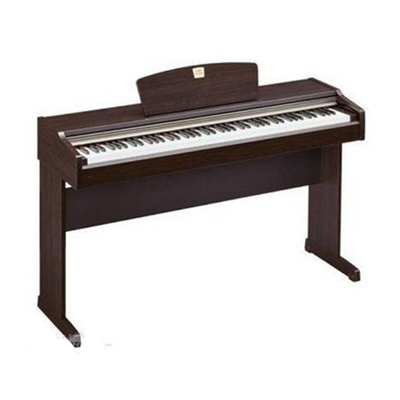
CLP-110
SERVICE MANUAL
CLP-110
I
CONTENTS
SPECIFICATIONS .............................................................................. 3
PANEL LAYOUT .................................................................................. 4
CIRCUIT BOARD LAYOUT ................................................................. 5
BLOCK DIAGRAM .............................................................................. 6
DISASSEMBLY PROCEDURE ........................................................... 7
LSI PIN DESCRIPTION .................................................................... 14
IC BLOCK DIAGRAM ........................................................................ 16
CIRCUIT BOARDS ........................................................................... 17
INSPECTION .................................................................................... 24
MIDI IMPLEMENTATION CHART ..................................................... 26
OVERALL CIRCUIT DIAGRAM
PARTS LIST
This document is printed on chlorine free (ECF) paper with soy ink.
CL 001675
HAMAMATSU, JAPAN
1.27K-389
Printed in Japan '02, 06
Advertisement
Chapters
Table of Contents

Related Manuals for Yamaha Clavinova CLP-110


Summary of Contents for Yamaha Clavinova CLP-110
- Page 1 CLP-110 SERVICE MANUAL CLP-110 CONTENTS SPECIFICATIONS ................3 PANEL LAYOUT .................. 4 CIRCUIT BOARD LAYOUT ..............5 BLOCK DIAGRAM ................6 DISASSEMBLY PROCEDURE ............7 LSI PIN DESCRIPTION ..............14 IC BLOCK DIAGRAM ................ 16 CIRCUIT BOARDS ................17 INSPECTION ..................24 MIDI IMPLEMENTATION CHART .............
- Page 2 IMPORTANT NOTICE This manual has been provided for the use of authorized Yamaha Retailers and their service personnel. It has been assumed that basic service procedures inherent to the industry, and more specifically Yamaha Products, are already known and understood by the users, and have therefore not been restated.
- Page 3 CLP-110 ATTACHING THE KEYBOARD STAND STABILIZERS (U Only) IMPORTANT! Be sure to attach the stabilizers to the keyboard stand prior to use to ensure maximum stability. Be sure to attach the stabilizers to the keyboard stand feet prior to assembly of the keyboard stand. Make sure that you have two stabilizers and four screws (one stabilizer for each of the keyboard stand feet and one 3.5X20mm screw and one 3.5X14mm screw for each of the stabilizers).
- Page 4 CLP-110 I PANEL LAYOUT Top Panel MIDI PHONES DAMPER PEDAL THRU MASTER VOLUME POWER DEMO METRONOME VOICE C0 D0 E0 F0 G0 A0 B0 C1 D1 E1 F1 G1 A1 B1 C2 D2 E2 F2 G2 A2 B2 C3 D3 E3 F3 G3 A3 B3 C4 D4 E4 F4 G4 A4 B4 C5 D5 E5 F5 G5 A5 B5 C6 D6 E6 F6 G6 A6 B6 C7 MASTER VOLUME DEMO...
- Page 5 CLP-110 I CIRCUIT BOARD LAYOUT...
- Page 6 +3.3D +3.3D...
- Page 7 CLP-110 I DISASSEMBLY PROCEDURE Top Board Assembly (Time required: about 1 min) Remove the four (4) screws marked [14]. (Fig.1) Slide the top board assembly forward and lift it out. [14] (Fig.1) [14]: Truss Head Tapping Screw-1 4.0X25 MFZN2BL (EN640160) Circuit Boards or Units in the Main Unit (Time required: about 6 min) Remove the top board assembly.
- Page 8 CLP-110 Key Cover Assembly Keycover Assembly Keycover Assembly (Time required: about 1 min) Remove the top board assembly. (See procedure 1) Cover the keyboards completely with the key cover assembly, and lift up the rear of it. (Fig.3) Lean the key cover assembly slightly and remove Side Cover the guide pin from the guide rail.
- Page 9 CLP-110 PN and VR Circuit Board (Time required: about 5 min) Remove the top board assembly. (See procedure 1) Remove the key cover assembly. (See procedure 3) Remove the end block assembly L. (See procedure 4) Remove the nine (9) screws marked [8]. (Fig.6) Remove the VR knob marked [7].
- Page 10 CLP-110 PL Circuit Board (Time required: about 7 min) Remove the top board assembly. (See procedure 1) Remove the key cover assembly. (See procedure 3) Remove the end block assembly (L, R). (See procedure 4) Remove the keyboard assembly. (See procedure 8) Remove the screw marked [T2f].
- Page 11 CLP-110 Side Cover Assembly (L, R) (Time required: about 10 min) For safety, this process should be done by two personnel. [S1] x 4 To remove screws from the bottom, prepare a worktable or bolsters to set the main unit. 12-1 Remove the top board assembly.
- Page 12 CLP-110 Disassembling the GHD Keyboard (Time required: about 20 min) After inserting a round stick (Rod: TX000670) between the frame and keys, remove the circuit boards. (Fig.16) 15-1 Remove the keyboard assembly. (See Procedure 8) 15-2 GH-D_SW L circuit board. Remove the seven (7) screws marked [260a].
- Page 13 CLP-110 Assembling the GHD Keyboard 16-1 Hammer of White (Black) Key Place the keyboard assembly upside down, insert a hammer assembly into the frame, and put the stopper L88W on. (Fig.19) There are four kinds of hammers that differ in weight. 16-2 Key Spring Place the keyboard assembly right side up, and fix a key spring to the frame by setting it at the slit and pushing it down once.
- Page 14 CLP-110 I LSI PIN DESCRIPTION CONTENTS HG73C205AFD XU947C00 SWX00B (TONE GENERATOR) ........15 UPD63200GS-E1 XP867A00 (D/A CONVERTER) ............. 16 YMZ702-D XR632A00 (KEY SCANNER) ..............16...
- Page 15 CLP-110 G HG73C205AFD (XU947C00) SWX00B TONE GENERATOR DM : IC001 NAME I/O FUNCTION NAME I/O FUNCTION Initial clear CMA3 RFCLKI PLL Clock CMA8 Program address bus PLL Control CMA2 4 AVDD_PLL Power supply read signal AVSS_PLL Ground CMA1 Program address bus MODE0 SWX dual mode high byte effective signal...
- Page 16 CLP-110 G UPD63200GS-E1 (XP867A00) DAC (Digital to Analog Converter) DM: IC004 NAME I/O FUNCTION NAME I/O FUNCTION 4/8 Fs selection R.REF Channel R voltage reference D.GND Digital ground L.REF Channel L voltage reference 16 BIT 16bit/18bit selection L.OUT Channel L output D.GND Digital power supply A.GND...
-
Page 17: Table Of Contents
CLP-110 I CIRCUIT BOARDS CONTENTS DM Circuit Board (2NA-V891010) ................18 AM Circuit Board (2NA-V891020) ................19, 20 D-JACK Circuit Board (2NA-V891030) ................. 21 HP Circuit Board (2NA-V541570) ................. 22 PN Circuit Board (2NA-V891040) ................. 22 PL Circuit Board (2NA-VN63760) ................. 22 VR Circuit Board (2NA-V902190) ................. -
Page 18: Gdm Circuit Board (2Na-V891010)
CLP-110 DM Circuit Board to D-JACK CN1 to D-JACK CN1 to AM CN2 to PN CN001 to GH-D_SW L CN1 Component Side Pattern Side 2NA-V891010... -
Page 19: Gam Circuit Board (2Na-V891020)
CLP-110 AM Circuit Board Component Side 2NA-V891020... - Page 20 CLP-110 AM Circuit Board Pattern Side 2NA-V891020...
-
Page 21: G D-Jack Circuit Board (2Na-V891030)
CLP-110 D-JACK Circuit Board MIDI DAMPER PEDAL THRU Component Side to DM CN2, CN3 Pattern Side 2NA-V891030... -
Page 22: Ghp Circuit Board (2Na-V541570)
CLP-110 HP Circuit Board PN Circuit Board DEMO METRONOME VOICE Component Side PHONES Component Side PL Circuit Board VR Circuit Board PILOT LAMP MASTER to HP CN2 VOLUME Component Side Component Side HP: 2NA-V541570 PL: 2NA-VN63760 PN: 2NA-V891040 VR: 2NA-V902190... -
Page 23: Gps Circuit Board (2Na-V001080)
CLP-110 to Power Switch PS Circuit Board PS: 2NA-V001080... - Page 24 CLP-110 I INSPECTION Preparation • To check the unit, following jigs are required. Level meter (with JIS-C Filter) Frequency counter Foot Pedal MIDI cable • Set each control as follows. (Fig.1) MASTER VOLUME: Max PEDAL: Except above: Default state of startup Connect the mesurement plug to the HEADPHONES jack.
- Page 25 CLP-110 Table 1 Test Items Item Test Function and Judgment criteria EQ Mid The sine wave of C4 sounds. Confirm that the output level of each jack is as follows. (Unit [dBm]) PHONES L, R -1.5 EQ High The sine wave of C6 sounds. Confirm that the output level of each jack is as follows.
- Page 26 CLP-110 I MIDI IMPLEMENTATION CHART YAMAHA [Clavinova] Date: 18 January, 2002 Model: CLP-110 MIDI Implementation Chart Version: 1.0 Function Transmitted Recognized Remarks Basic Default Channel Changed 1 - 16 1 - 16 Default Mode Messages Poly Mode only Altered *****************...
- Page 27 <P.1> CLP-110 CLP-110 CIRCUIT DIAGRAM (DM 1/1) PC2933T(XS516A00) REGULATOR +3.3V DM:IC007 SRAM 1M MASKROM 64M 1: V in 2: GND 3: V out NJM J78L05UA(XJ598A00) REGULATOR +5V DM:IC008 1: OUTPUT 2: COMMON 3: INPUT SWX00B to D-JACK-CN1 9pin to D-JACK-CN1 10pin to D-JACK-CN1 1-8pin REGULATOR +3.3V...
- Page 28 <P.2> CLP-110 CLP-110 CIRCUIT DIAGRAM (D-JACK, AM, PS, PN, VR, HP, PL) D-JACK MIDI INTERFACE PHOTO CUPLER POWER to DM-CN3 TRANSFORMER to DM-CN2 AC-IN * 1 AC-INLET to AM-CN1 28CC1-8812254 DAMPER PEDAL THRU µPC24M12AHF(XU387A00) 28CC1-8823353 1 REGULATOR +12V AM:IC001 1: INPUT REGULATOR +12V 2: GND 3: OUTPUT...
- Page 29 <P.3> CLP-110 CLP-110 CIRCUIT DIAGRAM (GH-D_SW H, GH-D_SW L) GH-D_SW H 28CC1-8811214 GH-D_SW L KSN2 Not install Install Not install Not install 28CC1-8811214 to DM-CN4 Note: See parts list for details of citcuit baord component parts. CLP-110 CLP-110...
- Page 30 CLP-110 CLP-110 PARTS LIST CONTENTS OVERALL ASSEMBLY ..........2 POWER SUPPLY UNIT ........... 15 MAIN UNIT ..............4 KEYBOARD ASSEMBLY ......... 16 SIDE BOARD ASSEMBLY ......... 8 A SHEET ASSEMBLY ..........18 TOP BOARD ASSEMBLY .......... 9 D-JACK ASSEMBLY ..........18 MUSIC REST ASSEMBLY ........
-
Page 31: Overall Assembly
CLP-110 I OVERALL ASSEMBLY Screw set Headphone hanger set Back Toe Set 3.5x20mm screws 3.5x14mm screws PART NO. DESCRIPTION REMARKS QTY RANK REF NO. OVERALL ASSEMBLY CLP-110 U,E,G,N Main Unit (V851290) Main Unit (V851300) Main Unit (V851310) Side Board Assembly-L CL LEFT (V862020) Side Board Assembly-R... - Page 32 CLP-110 DESCRIPTION REMARKS PART NO. QTY RANK REF NO. V3126300 AC Cord Set 2.5m VT016000 AC Cord Set 2.5m V3126500 AC Cord Set 2.5m V8740600 Headphone Hanger Set VT373000 Sustain Pedal Bench BC-100DR (V553140) *: New Parts RANK: Japan only...
- Page 33 CLP-110 I MAIN UNIT Rear view Top view 1 T7 T12 Side view T2 T2a...
- Page 34 CLP-110 Bottom view Top view 2 U Only U Only T6a T6b...
-
Page 35: Main Unit
CLP-110 DESCRIPTION REMARKS PART NO. QTY RANK REF NO. MAIN UNIT CLP-110 Main Unit (V851290) Main Unit (V851300) Main Unit (V851310) Main Unit Sub Assembly (V851320) Name Plate (V861970) Name Plate (V861980) (V862000) Name Plate V 0 0 1 0 3 0 0 Power Supply Unit V 0 0 1 0 4 0 0 Power Supply Unit... - Page 36 CLP-110 DESCRIPTION REMARKS PART NO. QTY RANK REF NO. VN637600 Circuit Board VU659100 Circuit Board VK099600 Connector Assembly 2P L=150 EP030240 Bind Head Tapping Screw-1 3.5X12 MFZN2Y EP030190 Bind Head Tapping Screw-1 3.5X16 MFZN2Y EP030190 Bind Head Tapping Screw-1 3.5X16 MFZN2Y V 9 0 7 3 5 0 0 Back Top Board Assembly Holder...
- Page 37 CLP-110 I SIDE BOARD ASSEMBLY Front view Side view PART NO. DESCRIPTION REMARKS QTY RANK REF NO. SIDE BOARD ASSEMBLY CLP-110 V 8 6 2 0 2 0 0 Side Board Assembly-L CL LEFT Side Board LEFT (V862040) Stand Base Assembly CL LEFT (V862090) Stand Base...
- Page 38 CLP-110 I TOP BOARD ASSEMBLY Top view Side view PART NO. DESCRIPTION REMARKS QTY RANK REF NO. TOP BOARD ASSEMBLY CLP-110 V 8 5 1 3 3 0 0 Top Board Assembly Top Board Assembly (V851340) V 2 7 8 0 4 0 0 Stopper Rail, Music Score VZ179200 PW Head Screw...
-
Page 39: Music Rest Assembly
CLP-110 I MUSIC REST ASSEMBLY Rear view Side view PART NO. DESCRIPTION REMARKS QTY RANK REF NO. MUSIC REST ASSEMBLY CLP-110 V 8 5 1 4 2 0 0 Music Rest Assembly Music Rest (V851430) V 8 4 3 7 6 0 0 Hinge 1STEP 1.6mm YMMA VV965900... -
Page 40: Side Cover Assembly
CLP-110 I SIDE COVER ASSEMBLY Front view Side view PART NO. DESCRIPTION REMARKS QTY RANK REF NO. SIDE COVER ASSEMBLY CLP-110 V 8 5 1 7 3 0 0 Side Cover Assembly CL LEFT Side Cover LEFT (V851760) V 8 5 1 8 1 0 0 Guide Rail LEFT EP030240... -
Page 41: End Block Assembly
CLP-110 I END BLOCK ASSEMBLY END BLOCK ASSEMBLY (L) END BLOCK ASSEMBLY (R) PART NO. DESCRIPTION REMARKS QTY RANK REF NO. END BLOCK ASSEMBLY CLP-110 End Block Assembly LEFT (V869920) V 8 7 2 8 4 0 0 End Block Sub Assembly-L LEFT Sub Angle P (V861560) -
Page 42: Panel Assembly
CLP-110 I PANEL ASSEMBLY Front view Top view Rear view PART NO. DESCRIPTION REMARKS QTY RANK REF NO. PANEL ASSEMBLY CLP-110 V 8 6 1 4 6 0 0 Panel Assembly Panel LEFT (V904060) Panel RIGHT (V904070) Panel C Assembly CENTER (V955960) V 5 9 9 3 4 0 0... -
Page 43: Key Cover Assembly
CLP-110 I KEY COVER ASSEMBLY Bottom view 2b 2c 2b 2c Top view PART NO. DESCRIPTION REMARKS QTY RANK REF NO. KEY COVER ASSEMBLY CLP-110 V 8 5 1 6 8 0 0 Key Cover Assembly Slide Cover 1300 (V851690) V 4 9 6 1 9 0 0 Sash Assembly FRONT... -
Page 44: Power Supply Unit
CLP-110 I POWER SUPPLY UNIT Top view Front view PART NO. DESCRIPTION REMARKS QTY RANK REF NO. POWER SUPPLY UNIT CLP-110 V 0 0 1 0 3 0 0 Power Supply Unit V 0 0 1 0 4 0 0 Power Supply Unit V 0 0 1 0 5 0 0 Power Supply Unit... - Page 45 CLP-110 I KEYBOARD ASSEMBLY...
-
Page 46: Keyboard Assembly
CLP-110 DESCRIPTION REMARKS PART NO. QTY RANK REF NO. KEYBOARD ASSEMBLY CLP-110 VZ705400 Keyboard Assembly A88 K6 MK Frame (VU42210) VU101000 White Key WHITE C VU101100 White Key WHITE D VU101200 White Key WHITE E VU101300 White Key WHITE F VU101400 White Key WHITE G... -
Page 47: A Sheet Assembly
CLP-110 I A SHEET ASSEMBLY Top view Front view Side view DESCRIPTION REMARKS PART NO. QTY RANK REF NO. A SHEET ASSEMBLY CLP-110 A Sheet Assembly (V907410) Holder, A Sheet (V906990) V 8 9 1 0 2 0 0 Circuit Board EP600130 Bind Head Tapping Screw-B 3.0X6 MFZN2Y... -
Page 48: Headphones Jack Assembly
CLP-110 I HEADPHONES JACK ASSEMBLY PART NO. DESCRIPTION REMARKS QTY RANK REF NO. HEADPHONES JACK ASSEMBLY CLP-110 Headphones Jack Assembly (V969120) V 5 4 1 5 7 0 0 Circuit Board VN631800 Angle, Headphone VB508600 Hexagonal Nut 12.0 14X2 MFZN2BL RANK: Japan only *: New Parts... -
Page 49: Sustain Pedal
CLP-110 I SUSTAIN PEDAL Pedal assembly PART NO. DESCRIPTION REMARKS QTY RANK REF NO. SUSTAIN PEDAL CLP-110 VT373000 Sustain Pedal Tube 4.1 AWG#6 (CH00217) Tube 5.2 AWG#4 (CH00219) EC030070 Flat Head Screw 3.0X8 MFZN2Y EE630060 Pan Head Screw 3.0X12 MFZN2Y CB806740 Pedal Box CB806750... -
Page 50: Bench
CLP-110 I BENCH Screw set x 4 (03761250) x 4 (03765820) PART NO. DESCRIPTION REMARKS QTY RANK REF NO. BENCH CLP-110 Bench BC-100DR (V553140) V 5 5 3 2 9 0 0 Bench Board Assembly BC-100DR Bench Board Assembly ROSE (V553350) Bench Side Frame Unit BC-100DR... -
Page 51: Electrical Parts
CLP-110 I ELECTRICAL PARTS DESCRIPTION REMARKS PART NO. QTY RANK REF NO. ELECTRICAL PARTS CLP-110 V 8 9 1 0 2 0 0 Circuit Board (XW981B0) V 8 9 1 0 1 0 0 Circuit Board (XW980A0) V 8 9 1 0 3 0 0 Circuit Board D-JACK (V903460)(X2588B0) - Page 52 CLP-110 DESCRIPTION REMARKS PART NO. QTY RANK REF NO. US035100 Ceramic Capacitor-B (chip) 0.1000 16V Z US135100 Ceramic Capacitor-F (chip) 0.1000 16V Z US135100 Ceramic Capacitor-F (chip) 0.1000 16V Z US064100 Ceramic Capacitor-B (chip) 0.0100 50V K US064100 Ceramic Capacitor-B (chip) 0.0100 50V K LB918050 Base Post Connector...
- Page 53 CLP-110 DESCRIPTION REMARKS PART NO. QTY RANK REF NO. US062100 Ceramic Capacitor-SL(chip) 100P 50V J US062100 Ceramic Capacitor-SL(chip) 100P 50V J US062100 Ceramic Capacitor-SL(chip) 100P 50V J US064100 Ceramic Capacitor-B (chip) 0.0100 50V K UF037100 Electrolytic Cap. (chip) 10 16V US064100 Ceramic Capacitor-B (chip) 0.0100 50V K...
- Page 54 CLP-110 DESCRIPTION REMARKS PART NO. QTY RANK REF NO. RD357470 Carbon Resistor (chip) 47.0K 63M J RD354470 Carbon Resistor (chip) 47.0 63M J RD357100 Carbon Resistor (chip) 10.0K 63M J RD357100 Carbon Resistor (chip) 10.0K 63M J RD350000 Carbon Resistor (chip) 0 63M J RD350000 Carbon Resistor (chip)
- Page 55 CLP-110 DESCRIPTION REMARKS PART NO. QTY RANK REF NO. RD356100 Carbon Resistor (chip) 1.0K 63M J RD355220 Carbon Resistor (chip) 220.0 63M J RD357100 Carbon Resistor (chip) 10.0K 63M J RD350000 Carbon Resistor (chip) 0 63M J RD350000 Carbon Resistor (chip) 0 63M J VV556400 Transistor...
- Page 56 CLP-110 DESCRIPTION REMARKS PART NO. QTY RANK REF NO. VV439800 SW003 Tact Switch SKQNAJ VOICE V 0 0 7 5 8 0 0 VR001 Rotary Variable Resistor A10.0K RK14K1240 MASTER VOLUME VN637600 Circuit Board (VN63740)(XL151B0) VB858100 Connector Base Post PH- 2P SE VD180000 SLZ-190B-03 RE POWER...
- Page 57 CLP-110 DESCRIPTION REMARKS PART NO. QTY RANK REF NO. XU445A00 Power Transformer J/UL/CSA A XU446A00 Power Transformer IEC65 E XU447A00 Power Transformer N IEC65 E VY846700 Rubber Contact GH 2M D0-C#1,D1-C#2,D2-C#3, D3-C#4,D4-C#5,D5-C#6 VY846800 Rubber Contact GH 2M A-1-C#0 VY846900 Rubber Contact GH 2M D6-C7 *: New Parts...
Need help?
Do you have a question about the Clavinova CLP-110 and is the answer not in the manual?
Questions and answers