Table of Contents
Advertisement
Quick Links
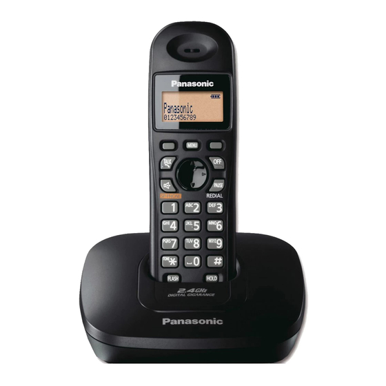
Telephone Equipment
KX-TG3611BXB
Model No.
KX-TG3611BXS
KX-TG3612BXB
KX-TG3612BXS
KX-TGA361BXB
KX-TGA361BXS
2.4 GHz Digital Cordless Phone
B: Black Version
S: Pearl White Version
(for Asia, Middle Near East and other areas)
© Panasonic Communications Co., Ltd. 2009.
Unauthorized copying and distribution is a violation
of law.
ORDER NO. KM40903838CE
Advertisement
Table of Contents
Troubleshooting


Need help?
Do you have a question about the KX-TG3611BXB and is the answer not in the manual?
Questions and answers