Table of Contents
Advertisement
Quick Links
Telephone Equipment
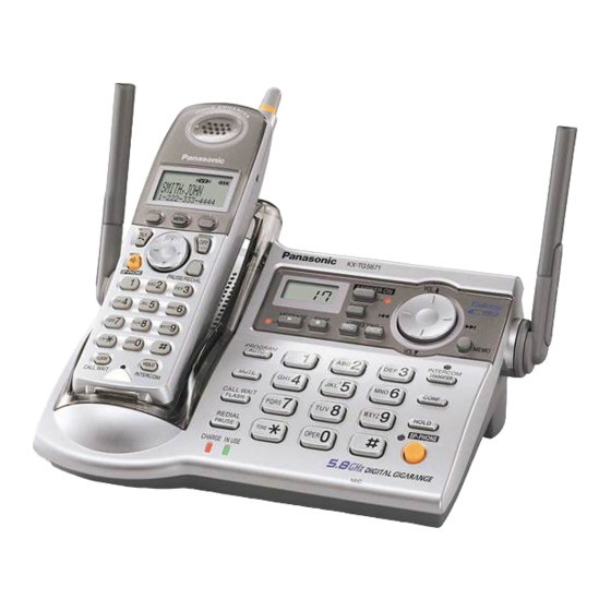
KX-TG5671S
KX-TG5672B
KX-TG5673B
KX-TGA560S
KX-TGA560B
5.8 GHz Digital Cordless Answering
System
Silver Version
Black Version
(for U.S.A.)
© 2006 Panasonic Communications Co., Ltd. All
rights
reserved.
distribution is a violation of law.
ORDER NO. KM40601971CE
F12
Unauthorized
copying
and
Advertisement
Table of Contents
Troubleshooting

Related Manuals for Panasonic KX-TG5671S


Summary of Contents for Panasonic KX-TG5671S
- Page 1 ORDER NO. KM40601971CE Telephone Equipment KX-TG5671S KX-TG5672B KX-TG5673B KX-TGA560S KX-TGA560B 5.8 GHz Digital Cordless Answering System Silver Version Black Version (for U.S.A.) © 2006 Panasonic Communications Co., Ltd. All rights reserved. Unauthorized copying distribution is a violation of law.
-
Page 2: Table Of Contents
KX-TG5671S / KX-TG5672B / KX-TG5673B / KX-TGA560S / KX-TGA560B Note: Because CONTENTS 4 is the extract from the Operating Instructions of this model, it is subject to change without notice. You can download and refer to the original Operating Instructions on TSN Server for further information. - Page 3 KX-TG5671S / KX-TG5672B / KX-TG5673B / KX-TGA560S / KX-TGA560B 17.6. Reception Signal 29.2. Handset 18 CIRCUIT OPERATION (CHARGER UNIT) 29.3. Charger Unit 19 SIGNAL ROUTE 29.4. Accessories and Packing Materials 20 CPU DATA (BASE UNIT) 29.5. Fixtures and Tools 20.1. IC501...
-
Page 4: About Lead Free Solder (Pbf: Pb Free)
KX-TG5671S / KX-TG5672B / KX-TG5673B / KX-TGA560S / KX-TGA560B 1 ABOUT LEAD FREE SOLDER (PbF: Pb free) Note: In the information below, Pb, the symbol for lead in the periodic table of elements, will refer to standard solder or solder that contains lead. -
Page 5: How To Recognize That Pb Free Solder Is Used
KX-TG5671S / KX-TG5672B / KX-TG5673B / KX-TGA560S / KX-TGA560B 1.2. How to Recognize that Pb Free Solder is Used (Example: Handset P.C.B.) Marked IC851 IC246 IC701 IC801 IC201 IC241 (Component View) Note: The location of the “PbF” mark is subject to change without notice. -
Page 6: For Service Technicians
KX-TG5671S / KX-TG5672B / KX-TG5673B / KX-TGA560S / KX-TGA560B 2 FOR SERVICE TECHNICIANS ICs and LSIs are vulnerable to static electricity. When repairing, the following precautions will help prevent recurring malfunctions. 1. Cover plastic parts boxes with aluminum foil. 2. Ground the soldering irons. -
Page 7: Operating Instructions
KX-TG5671S / KX-TG5672B / KX-TG5673B / KX-TGA560S / KX-TGA560B 4 OPERATING INSTRUCTIONS 4.1. Battery 4.1.1. Battery Installation/Replacement 4.1.2. Battery Charge Note for service: The battery strength may not be indicated correctly if the battery is disconnected and connected again, even after it is fully... - Page 8 KX-TG5671S / KX-TG5672B / KX-TG5673B / KX-TGA560S / KX-TGA560B 4.1.3. Battery Level 4.1.4. Panasonic Battery Performance...
-
Page 9: Location Of Controls
KX-TG5671S / KX-TG5672B / KX-TG5673B / KX-TGA560S / KX-TGA560B 4.2. Location of Controls 4.2.1. Base Unit... - Page 10 KX-TG5671S / KX-TG5672B / KX-TG5673B / KX-TGA560S / KX-TGA560B 4.2.2. Handset...
-
Page 11: Displays
KX-TG5671S / KX-TG5672B / KX-TG5673B / KX-TGA560S / KX-TGA560B 4.3. Displays 4.3.1. Display Items... - Page 12 KX-TG5671S / KX-TG5672B / KX-TG5673B / KX-TGA560S / KX-TGA560B 4.3.2. Troubleshooting (Handset LCD)
-
Page 13: Settings
KX-TG5671S / KX-TG5672B / KX-TG5673B / KX-TGA560S / KX-TGA560B 4.4. Settings 4.4.1. Connecting the AC Adaptor and Telephone Line Cord... - Page 14 KX-TG5671S / KX-TG5672B / KX-TG5673B / KX-TGA560S / KX-TGA560B 4.4.2. Connecting the Charger (KX-TG5672/KX-TG5673 only)
- Page 15 KX-TG5671S / KX-TG5672B / KX-TG5673B / KX-TGA560S / KX-TGA560B 4.4.3. Programmable Settings 4.4.3.1. Programming by Scrolling through the Display Menus...
- Page 16 KX-TG5671S / KX-TG5672B / KX-TG5673B / KX-TGA560S / KX-TGA560B 4.4.3.2. Programming Using the Direct Commands...
- Page 17 KX-TG5671S / KX-TG5672B / KX-TG5673B / KX-TGA560S / KX-TGA560B...
-
Page 18: Troubleshooting
KX-TG5671S / KX-TG5672B / KX-TG5673B / KX-TGA560S / KX-TGA560B 4.5. Troubleshooting If the handset display shows error messages, see “Troubleshooting (Handset LCD) (P.12)” for the Cause & Solution. - Page 19 KX-TG5671S / KX-TG5672B / KX-TG5673B / KX-TGA560S / KX-TGA560B...
- Page 20 KX-TG5671S / KX-TG5672B / KX-TG5673B / KX-TGA560S / KX-TGA560B...
- Page 21 KX-TG5671S / KX-TG5672B / KX-TG5673B / KX-TGA560S / KX-TGA560B...
-
Page 22: Disassembly Instructions
KX-TG5671S / KX-TG5672B / KX-TG5673B / KX-TGA560S / KX-TGA560B 5 DISASSEMBLY INSTRUCTIONS 5.1. Base Unit Shown in Fig.- To Remove - Remove - Cabinet Cover Screws (2.6 × 12)..(A) × 5 Main P. C. Board Tapes, Solders and Cable Main P. C. Board Operational P. -
Page 23: Handset
KX-TG5671S / KX-TG5672B / KX-TG5673B / KX-TGA560S / KX-TGA560B 5.2. Handset Shown in Fig.- To Remove - Remove - Cabinet Cover Screws (2 × 14)..(C) × 2 Follow the procedure. Main P. C. Board Tape and Solders Screws (2 × 9).....(D ) × 3... -
Page 24: Charger Unit
KX-TG5671S / KX-TG5672B / KX-TG5673B / KX-TGA560S / KX-TGA560B 5.3. Charger Unit Shown in Fig.- To Remove - Remove - Cabinet Cover Screws (2.6 × 12)..(E) × 2 Main P.C.Board Main P.C.Board... -
Page 25: How To Replace The Handset Lcd
KX-TG5671S / KX-TG5672B / KX-TG5673B / KX-TGA560S / KX-TGA560B 6 HOW TO REPLACE THE HANDSET LCD... -
Page 26: Troubleshooting Guide
KX-TG5671S / KX-TG5672B / KX-TG5673B / KX-TGA560S / KX-TGA560B 7 TROUBLESHOOTING GUIDE Cross Reference: Note: Check Power (P.27) (*1) When a user claims that the unit disconnects a call right after the greeting message and no incoming Error Message Table (P.27) messages can be recorded, this symptom can not be Check Playback (P.29) -
Page 27: Check Power
KX-TG5671S / KX-TG5672B / KX-TG5673B / KX-TGA560S / KX-TGA560B 7.1. Check Power Cross Reference: Note: Power Supply Circuit (P.60) Flash Memory is IC601. Reset Circuit (P.62) DSP is IC501. (*1) Refer to “SPECIFICATION” on cover page for part number and supply voltage of AC adaptor. -
Page 28: Check Record
KX-TG5671S / KX-TG5672B / KX-TG5673B / KX-TGA560S / KX-TGA560B 7.3. Check Record BASE UNIT A) Not record Greeting Message B) Not record Incoming Message C) How to change the Auto Disconnect activation (time) Some Telephone Company lines (fiber or cable) ON Hook and OFF Hook voltages are lower than conventional lines, which may cause a malfunction of Auto Disconnect detection. -
Page 29: Check Playback
KX-TG5671S / KX-TG5672B / KX-TG5673B / KX-TGA560S / KX-TGA560B 7.4. Check Playback Cross Reference: Note: Power Supply Circuit (P.60) Flash Memory is IC601. DSP is IC501. 7.5. Check Sp-phone Transmission Cross Reference: Note: SIGNAL ROUTE (P.81) Flash Memory is IC601. -
Page 30: Check Sp-Phone Reception
KX-TG5671S / KX-TG5672B / KX-TG5673B / KX-TGA560S / KX-TGA560B 7.6. Check Sp-phone Reception Cross Reference: Note: Telephone Line Interface (P.63) Flash Memory is IC601. SIGNAL ROUTE (P.81) DSP is IC501. 7.7. Check Battery Charge Note: Flash Memory is IC601. DSP is IC501. -
Page 31: Check Link
KX-TG5671S / KX-TG5672B / KX-TG5673B / KX-TGA560S / KX-TGA560B 7.8. Check Link Note: Flash Memory is IC601. DSP is IC501. (*1) Refer to Finding out the Defective part (P.32). Cross Reference: Check the RF part (P.32) -
Page 32: Check The Rf Part
KX-TG5671S / KX-TG5672B / KX-TG5673B / KX-TGA560S / KX-TGA560B 7.9. Check the RF part 7.9.1. Finding out the Defective part After All the Checkings or Repairing 1. Re-register the checked Handset to the checked Base Unit, and Regular HS to Regular BU. - Page 33 KX-TG5671S / KX-TG5672B / KX-TG5673B / KX-TGA560S / KX-TGA560B 7.9.1.1. Registering a Handset...
- Page 34 KX-TG5671S / KX-TG5672B / KX-TG5673B / KX-TGA560S / KX-TGA560B 7.9.2. RF Check Flowchart Each item (1 ~ 6) of RF Check Flowchart corresponds to Check Table for RF part (P.35). Please refer to the each item.
- Page 35 KX-TG5671S / KX-TG5672B / KX-TG5673B / KX-TGA560S / KX-TGA560B 7.9.3. Check Table for RF part Item BU (Base Unit) Check HS (HandSet) Check Link Confirmation Normal 1. Register Regular HS to BU (to be checked). 1. Register HS (to be checked) to Regular BU.
- Page 36 KX-TG5671S / KX-TG5672B / KX-TG5673B / KX-TGA560S / KX-TGA560B 7.9.4. TEST RANGE Check Circuit block which range is defective can be found by the following check. Item BU (Base Unit) Check HS (HandSet) Check Range Confirmation TX 1. Register Regular HS to BU (to be checked).
- Page 37 KX-TG5671S / KX-TG5672B / KX-TG5673B / KX-TGA560S / KX-TGA560B 7.9.5. RF-DSP Interface Signal Wave Form <Test Burst Mode>...
- Page 38 KX-TG5671S / KX-TG5672B / KX-TG5673B / KX-TGA560S / KX-TGA560B <Test Burst Mode>...
-
Page 39: Check Handset Transmission
KX-TG5671S / KX-TG5672B / KX-TG5673B / KX-TGA560S / KX-TGA560B 7.10. Check Handset Transmission Cross Reference: SIGNAL ROUTE (P.81). 7.11. Check Handset Reception Cross Reference: SIGNAL ROUTE (P.81). Note: When checking the RF part, Refer to Check the RF part (P.32) 7.12. -
Page 40: Adjustment And Test Mode
KX-TG5671S / KX-TG5672B / KX-TG5673B / KX-TGA560S / KX-TGA560B 8 ADJUSTMENT AND TEST MODE 8.1. Test Mode Flow Chart for Base Unit 8.1.1. Test Burst Mode Note: (*1) LCD displays the Channel number. (*2) Refer to Check Table for RF part (P.35) and RX-CW Test Mode (P.45) for proper Handset settings. - Page 41 KX-TG5671S / KX-TG5672B / KX-TG5673B / KX-TGA560S / KX-TGA560B 8.1.2. RX-CW Test Mode Note: (*1) LCD displays the Channel number. (*2) Refer to Check Table for RF part (P.35) and Test Burst Mode (P.44) for proper Handset settings.
- Page 42 KX-TG5671S / KX-TG5672B / KX-TG5673B / KX-TGA560S / KX-TGA560B 8.1.3. Test Link Mode Note: (*1) LCD displays the Channel number. (*2) LCD displays the number of selected power. (*3) Refer to Check Table for RF part (P.35) and Test Link Mode (P.46) for proper Handset settings.
- Page 43 KX-TG5671S / KX-TG5672B / KX-TG5673B / KX-TGA560S / KX-TGA560B 8.1.4. Adjustment Mode Cross Reference Check and Adjust X501 (Base Unit) Frequency (P.48) Note: (*1) This is an adjustment value (hex.).
-
Page 44: Test Mode Flow Chart For Handset
KX-TG5671S / KX-TG5672B / KX-TG5673B / KX-TGA560S / KX-TGA560B 8.2. Test Mode Flow Chart for Handset 8.2.1. Test Burst Mode Note: (*1) LCD displays the Channel number. (exception: default/ CH00 = 1ch.) (*2) Refer to Check Table for RF part (P.35) and RX-CW Test Mode (P.41) for proper Base Unit settings. - Page 45 KX-TG5671S / KX-TG5672B / KX-TG5673B / KX-TGA560S / KX-TGA560B 8.2.2. RX-CW Test Mode Note: (*1) LCD displays the Channel number. (exception: default/ CH00 = 1ch.) (*2) Refer to Check Table for RF part (P.35) and Test Burst Mode (P.40) for proper Base Unit settings.
- Page 46 KX-TG5671S / KX-TG5672B / KX-TG5673B / KX-TGA560S / KX-TGA560B 8.2.3. Test Link Mode Note: (*1) LCD displays the Channel number. (exception: default/ CH00 = 1ch.) (*2) for factory use only. (*3) Refer to Check Table for RF part (P.35) and Test Link Mode (P.42) for proper Base Unit settings.
- Page 47 KX-TG5671S / KX-TG5672B / KX-TG5673B / KX-TGA560S / KX-TGA560B 8.2.4. Adjustment Mode Cross Reference (*1) Adjust Battery Low Detector Voltage (Handset) (P.48) Note: (*2) These are the default values. (*3) These values may not be fixed depending on the battery strength.
-
Page 48: X501 (Base Unit), X201 (Handset) Check
KX-TG5671S / KX-TG5672B / KX-TG5673B / KX-TGA560S / KX-TGA560B 8.3. X501 (Base Unit), X201 (Handset) Check Equipment: Frequency counter Check Point for measurement: BCK Checking tolerance: 13.824MHz ± 270Hz (Base Unit)/13.824MHz ± 100Hz (Handset) 8.3.1. Check and Adjust X501 (Base Unit) Frequency 1. -
Page 49: Base Unit Reference Drawing
KX-TG5671S / KX-TG5672B / KX-TG5673B / KX-TGA560S / KX-TGA560B CN661 L102 L101 Q142 Q156 P101 Q141 Q161... -
Page 50: Handset Reference Drawing
KX-TG5671S / KX-TG5672B / KX-TG5673B / KX-TGA560S / KX-TGA560B... -
Page 51: Frequency Table
KX-TG5671S / KX-TG5672B / KX-TG5673B / KX-TGA560S / KX-TGA560B 8.7. Frequency Table 8.7.1. Base Unit Channel TX/RX Frequency (MHz) Channel TX/RX Frequency (MHz) Channel TX/RX Frequency (MHz) 5759.702398 5788.242242 5816.782086 5760.592291 5789.132135 5817.671978 5761.486139 5790.025982 5818.565826 5762.376031 5790.915875 5819.455719 5763.269879 5791.809723... - Page 52 KX-TG5671S / KX-TG5672B / KX-TG5673B / KX-TGA560S / KX-TGA560B 8.7.2. Handset Channel TX/RX Frequency (MHz) Channel TX/RX Frequency (MHz) Channel TX/RX Frequency (MHz) 5759.700425 5788.240269 5816.780113 5760.594273 5789.134117 5817.673960 5761.484165 5790.024009 5818.563853 5762.378013 5790.917857 5819.457701 5763.267906 5791.807749 5820.347593 5764.161753 5792.701597 5821.241441...
-
Page 53: How To Clear User Setting
KX-TG5671S / KX-TG5672B / KX-TG5673B / KX-TGA560S / KX-TGA560B 8.8. How to Clear User Setting Units are reset to the Factory settings by this operation (Erase recorded Voice messages, stored Phone numbers, Caller list and etc.). This operation should not be performed for a usual repair. -
Page 54: Description
KX-TG5671S / KX-TG5672B / KX-TG5673B / KX-TGA560S / KX-TGA560B 9 DESCRIPTION 9.1. Frequency The frequency range of 5.76GHz-5.84GHz is used. Transmitting and receiving channel between Base Unit and Handset is same frequency. Refer to Frequency Table (P.51). 9.2. FHSS (Frequency Hopping Spread Spectrum) This telephone is using an IC chip which has similar specification to WDCT (World Digital Cordless Telephone) and is the telephone system that can use multiple portable unit simultaneously. - Page 55 KX-TG5671S / KX-TG5672B / KX-TG5673B / KX-TGA560S / KX-TGA560B 9.2.1. TDD Frame Format Sync Field (72bit): Preamble 56bit + SyncWord 16bit Base Unit (Handset) adjusts the timing of reception so that reception of Base Unit (Handset) can correspond to transmission of Handset (Base Unit).
-
Page 56: Signal Flowchart In The Whole System
KX-TG5671S / KX-TG5672B / KX-TG5673B / KX-TGA560S / KX-TGA560B 9.3. Signal Flowchart in the Whole System Reception CN101 of the Base Unit is connected to the TEL line, and signal is enter through the bridge diode D101. While talking, the relay (Q141) is turned ON and amplified at the Q171, then led to DSP (IC501). -
Page 57: Explanation Of Link Data Communication
KX-TG5671S / KX-TG5672B / KX-TG5673B / KX-TGA560S / KX-TGA560B 10 EXPLANATION OF LINK DATA COMMUNICATION 10.1. Calling 10.2. To Terminate Communication 10.3. Ringing... - Page 58 KX-TG5671S / KX-TG5672B / KX-TG5673B / KX-TGA560S / KX-TGA560B...
-
Page 59: Circuit Operation (Base Unit_Main)
KX-TG5671S / KX-TG5672B / KX-TG5673B / KX-TGA560S / KX-TGA560B 12 CIRCUIT OPERATION (BASE UNIT_MAIN) General Description: (DSP, Flash Memory) is a digital speech/signal processing system that implements all the functions of speech compression, record and playback, and memory management required in a digital telephone answering machine. -
Page 60: Power Supply Circuit
KX-TG5671S / KX-TG5672B / KX-TG5673B / KX-TGA560S / KX-TGA560B 12.3. Power Supply Circuit Function: The power supply voltage from AC adaptor is converted to the desired voltage of each block. Circuit Operation: • • • • Q300 and IC300: 4.0V DCDC Converter... - Page 61 KX-TG5671S / KX-TG5672B / KX-TG5673B / KX-TGA560S / KX-TGA560B 12.3.1. Charge Circuit The voltage from the AC adaptor is supplied to the charge circuits. Main charge (130 ~ 220mA at the Battery) of maximum 7- hours is started soon after the Handset is placed on the Base Unit. Then it changes to Trickle charge to prevent from overcharging.
-
Page 62: Reset Circuit
KX-TG5671S / KX-TG5672B / KX-TG5673B / KX-TGA560S / KX-TGA560B 12.4. Reset Circuit Function: This circuit is used to initialize the microcomputer when it incorporates an AC adaptor. Circuit Operation: When the AC Adaptor is inserted into the unit, then the voltage is shifted by IC331 and power is supplied to the DSP. -
Page 63: Telephone Line Interface
KX-TG5671S / KX-TG5672B / KX-TG5673B / KX-TGA560S / KX-TGA560B 12.5. Telephone Line Interface Telephone Line Interface Circuit: Function • • • • Bell signal detection • • • • ON/OFF hook and pulse dial circuit • • • • Side tone circuit Bell signal detection and OFF HOOK circuit: In the idle mode, Q141 is open to cut the DC loop current and decrease the ring load. -
Page 64: Auto Disconnect Circuit
KX-TG5671S / KX-TG5672B / KX-TG5673B / KX-TGA560S / KX-TGA560B 12.6. Auto Disconnect Circuit Function: This circuit is used to detect the fact that another telephone connected to the same line is OFF-HOOK while the unit is in a receiving status or OGM transmitting status. -
Page 65: Parallel Connection Detect Circuit
KX-TG5671S / KX-TG5672B / KX-TG5673B / KX-TGA560S / KX-TGA560B 12.7. Parallel Connection Detect Circuit Function: In order to disable call waiting and stutter tone functions when using telephones connected in parallel, it is necessary to have a circuit that judges whether a telephone connected in parallel is in use or not. This circuit determines whether the telephone connected in parallel is on hook or off hook by detecting changes in the T/R voltage. -
Page 66: Calling Line Identification (Caller Id)/Call Waiting Caller Id
KX-TG5671S / KX-TG5672B / KX-TG5673B / KX-TGA560S / KX-TGA560B 12.8. Calling Line Identification (Caller ID)/Call Waiting Caller ID Function: Caller ID The caller ID is a chargeable ID which the user of a telephone circuit obtains by entering a contract with the telephone company to utilize a caller ID service. - Page 67 KX-TG5671S / KX-TG5672B / KX-TG5673B / KX-TGA560S / KX-TGA560B Call Waiting Caller ID Calling Identity Delivery on Call Waiting (CIDCW) is a CLASS service that allows a customer, while off-hook on an existing call, to receive information about a calling party on a waited call. The transmission of the calling information takes place almost immediately after the customer is alerted to the new call so he/she can use this information to decide whether to take the new call.
- Page 68 KX-TG5671S / KX-TG5672B / KX-TG5673B / KX-TGA560S / KX-TGA560B TC_CTRL RSTN RXEN TXEN REFIN RXGAIN RXEN TXEN 5.8GHz...
- Page 69 KX-TG5671S / KX-TG5672B / KX-TG5673B / KX-TGA560S / KX-TGA560B TC_CTRL RSTN RXEN TXEN REFIN RXGAIN RXEN TXEN 5.8GHz...
-
Page 70: Circuit Operation (Rf Part)
KX-TG5671S / KX-TG5672B / KX-TG5673B / KX-TGA560S / KX-TGA560B 15 CIRCUIT OPERATION (RF PART) General Description: RF part includes Transmitter and Receiver functions. Digital signals (Mainly voice data) that come from DSP, are modulated and are transmitted. On the other hand, received signals are demodulated and go out to DSP. -
Page 71: Power Supply Circuit
KX-TG5671S / KX-TG5672B / KX-TG5673B / KX-TGA560S / KX-TGA560B 15.1. Power Supply Circuit As indicated below, the various voltages are supplied to each block. V_PA, about 4.0V at Base Unit or 3.3V at Handset, is supplied to the Power amplifier in 5.8GHz PA circuit. -
Page 72: Ghz Mod/Demod Circuit
KX-TG5671S / KX-TG5672B / KX-TG5673B / KX-TGA560S / KX-TGA560B 15.2. 2.4GHz Mod/Demod Circuit IC701 incorporates all of the modulation and demodulation functions. TX Digital data (TX_DATA) from DSP is supplied to pin 27 of IC701, and then 2.4GHz TX modulated signal is output from pin1. This TX signal goes into the 5.8GHz Converter circuit. 2.4GHz RX signal from 5.8GHz Converter circuit is passed through matching circuit and supplied to pin4 of IC701, then demodulated signal... -
Page 73: Ghz Converter Circuit
KX-TG5671S / KX-TG5672B / KX-TG5673B / KX-TGA560S / KX-TGA560B 15.3. 5.8GHz Converter Circuit This block converts frequency of TX signal and RX signal. IC801 includes TX-MIXER, RX-MIXER, PLL and VCO modules internally. The VCO module is tuned by PLL synthesizer module, and generates 3.4GHz Local signal. Reference clock (13.824MHz) from DSP block is supplied to pin7 of IC701. -
Page 74: Ghz Pa (Power Amplifier), 5.8Ghz Lna
KX-TG5671S / KX-TG5672B / KX-TG5673B / KX-TGA560S / KX-TGA560B 15.4. 5.8GHz PA (Power Amplifier), 5.8GHz LNA (Low Noise Amplifier) and Antenna Switch Circuit PA block amplifies power of 5.8GHz TX signal. 5.8GHz TX signal from 5.8GHz Converter circuit is filtered by 5.8GHz-BPF FL811, and amplified by Power amplifier (PA) block of IC851. -
Page 75: Block Diagram (Handset)
KX-TG5671S / KX-TG5672B / KX-TG5673B / KX-TGA560S / KX-TGA560B 16 BLOCK DIAGRAM (HANDSET) IC241 X201 EEPROM 13.824MHz Q231 CHG_DET CHARGE DETECT OSC-IN Q362, Q363 RF part TX_DATA RX_DATA CHARGE CHG_CTL PA_CONT CONTROL RADIO_EN CON_EN Q221 SYN_LE2 SYN_OUT RESET RESET SYN_DATA... -
Page 76: Circuit Operation (Handset)
KX-TG5671S / KX-TG5672B / KX-TG5673B / KX-TGA560S / KX-TGA560B 17 CIRCUIT OPERATION (HANDSET) 17.1. Construction The circuit mainly consists of DSP and RF part as shown in the block diagram. 17.1.1. DSP: IC201 Function • • • • Battery Low, Power down detect circuit •... -
Page 77: Power Supply Circuit
KX-TG5671S / KX-TG5672B / KX-TG5673B / KX-TGA560S / KX-TGA560B 17.2. Power Supply Circuit Voltage is supplied separately to each block. -
Page 78: Charge Circuit
KX-TG5671S / KX-TG5672B / KX-TG5673B / KX-TGA560S / KX-TGA560B 17.3. Charge Circuit When the Handset is put on the cradle of the Base Unit or the charger, the power is supplied from CHARGE+ and CHARGE- terminals to charge the battery via D353 and R366 or Q361. The voltage between CHARGE+ and CHARGE- flows R231 →... -
Page 79: Sending Signal
KX-TG5671S / KX-TG5672B / KX-TG5673B / KX-TGA560S / KX-TGA560B 17.5. Sending Signal The voice signal from the microphone is input to DSP (90, 91). CN331 is the headset jack. When the headphone is connected, the Q331 detect it. The input from the microphone of the Handset (MIN, MIP) is cut and the microphone signal from the headset is input to DSP (95). -
Page 80: Circuit Operation (Charger Unit)
KX-TG5671S / KX-TG5672B / KX-TG5673B / KX-TGA560S / KX-TGA560B 18 CIRCUIT OPERATION (CHARGER UNIT) The voltage from the AC adaptor is supplied to the charge circuits. Main charge (130 ~ 220mA at the Battery) of maximum 7- hours is started soon after the Handset is placed on the Charger Unit. Then it changes to Trickle charge to prevent from overcharging. -
Page 81: Signal Route
KX-TG5671S / KX-TG5672B / KX-TG5673B / KX-TGA560S / KX-TGA560B 19 SIGNAL ROUTE Each signal route is as follows. - Page 82 KX-TG5671S / KX-TG5672B / KX-TG5673B / KX-TGA560S / KX-TGA560B Each signal route is as follows. RF part signal route...
-
Page 83: Cpu Data (Base Unit)
KX-TG5671S / KX-TG5672B / KX-TG5673B / KX-TGA560S / KX-TGA560B 20 CPU DATA (BASE UNIT) 20.1. IC501 Description High High_Z Description High High_Z GNDPA 63 KEY_IN3 Key In SPOUTP 64 KEY_IN2 Key In BMCCLK 65 KEY_IN1 Key In TXMOD 66 GND... -
Page 84: Cpu Data (Handset)
KX-TG5671S / KX-TG5672B / KX-TG5673B / KX-TGA560S / KX-TGA560B 21 CPU DATA (HANDSET) 21.1. IC201 Description High High_Z Description High High_Z GNDPA 61 ANT_LED2 SPOUTP 62 ANT_LED3 BCLK 63 KEYSTROBE_E Active RSSI 64 KEYSTROBE_D Active 65 KEYSTROBE_C Active XOUT 66 KEYSTROBE_B... -
Page 85: Explanation Of Ic Terminals (Rf Part)
KX-TG5671S / KX-TG5672B / KX-TG5673B / KX-TGA560S / KX-TGA560B 22 EXPLANATION OF IC TERMINALS (RF PART) 22.1. IC701... -
Page 86: Ic801
KX-TG5671S / KX-TG5672B / KX-TG5673B / KX-TGA560S / KX-TGA560B 22.2. IC801 Backside Terminal: GND... -
Page 87: Ic851
KX-TG5671S / KX-TG5672B / KX-TG5673B / KX-TGA560S / KX-TGA560B 22.3. IC851 Backside Terminal: GND... -
Page 88: How To Replace The Flat Package Ic
KX-TG5671S / KX-TG5672B / KX-TG5673B / KX-TGA560S / KX-TGA560B 23 HOW TO REPLACE THE FLAT PACKAGE IC Even if you do not have the special tools (for example, a spot heater) to remove the Flat IC, with some solder (large amount), a soldering iron and a cutter knife, you can easily remove the ICs that have more than 100 pins. -
Page 89: Flat Package Ic Installation Procedure
KX-TG5671S / KX-TG5672B / KX-TG5673B / KX-TGA560S / KX-TGA560B 23.3. FLAT PACKAGE IC INSTALLATION PROCEDURE 1. Temporarily fix the FLAT PACKAGE IC, soldering the two marked pins. *Check the accuracy of the IC setting with the corresponding soldering foil. 2. Apply flux to all pins of the FLAT PACKAGE IC. -
Page 90: Cabinet And Electrical Parts (Base Unit)
KX-TG5671S / KX-TG5672B / KX-TG5673B / KX-TGA560S / KX-TGA560B 24 CABINET AND ELECTRICAL PARTS (BASE UNIT) Note: (*1) for KX-TG5671... -
Page 91: Cabinet And Electrical Parts (Handset)
KX-TG5671S / KX-TG5672B / KX-TG5673B / KX-TGA560S / KX-TGA560B 25 CABINET AND ELECTRICAL PARTS (HANDSET) Note: (*1) Attach the cushion (No. 126) to the exact location described above. (*2) This cable is fixed by welding. Refer to HOW TO REPLACE THE HANDSET LCD (P.25). -
Page 92: Cabinet And Electrical Parts (Charger Unit)
KX-TG5671S / KX-TG5672B / KX-TG5673B / KX-TGA560S / KX-TGA560B 26 CABINET AND ELECTRICAL PARTS (CHARGER UNIT) -
Page 93: Accessories And Packing Materials
KX-TG5671S / KX-TG5672B / KX-TG5673B / KX-TGA560S / KX-TGA560B 27 ACCESSORIES AND PACKING MATERIALS 27.1. KX-TG5671S... -
Page 94: Kx-Tg5672B
KX-TG5671S / KX-TG5672B / KX-TG5673B / KX-TGA560S / KX-TGA560B 27.2. KX-TG5672B... -
Page 95: Kx-Tg5673B
KX-TG5671S / KX-TG5672B / KX-TG5673B / KX-TGA560S / KX-TGA560B 27.3. KX-TG5673B... -
Page 96: Kx-Tga560B
KX-TG5671S / KX-TG5672B / KX-TG5673B / KX-TGA560S / KX-TGA560B 27.4. KX-TGA560B... -
Page 97: Terminal Guide Of The Ics, Transistors And Diodes
KX-TG5671S / KX-TG5672B / KX-TG5673B / KX-TGA560S / KX-TGA560B 28 TERMINAL GUIDE OF THE ICs, TRANSISTORS AND DIODES 28.1. Base Unit 28.2. Handset... -
Page 98: Replacement Parts List
KX-TG5671S / KX-TG5672B / KX-TG5673B / KX-TGA560S / KX-TGA560B 29 REPLACEMENT PARTS LIST Note: Ref. Part No. Part Name & Description Remarks 1. RTL (Retention Time Limited) PQKM10660Q2 CABINET BODY (for KX-TG5671S) PS-HB The marking (RTL) indicates that the Retention Time is... - Page 99 KX-TG5671S / KX-TG5672B / KX-TG5673B / KX-TGA560S / KX-TGA560B Ref. Part No. Part Name & Description Remarks Ref. Part No. Part Name & Description Remarks Q535 2SD1819A TRANSISTOR(SI) R340 ERJ3GEYJ123 (DIODES) R341 ERJ3GEYJ102 D101 PQVDMD5S DIODE(SI) R342 ERJ3GEYJ473 D113 MA111...
-
Page 100: Handset
KX-TG5671S / KX-TG5672B / KX-TG5673B / KX-TGA560S / KX-TGA560B Ref. Part No. Part Name & Description Remarks Ref. Part No. Part Name & Description Remarks C304 ECUV1A105KBV C747 ECJ0EC1H100D C305 ECUV1H103KBV 0.01 C748 ECJ0EC1H101J 100P C306 F2G1E1010011 C749 ECJ0EC1H101J 100P... - Page 101 KX-TG5671S / KX-TG5672B / KX-TG5673B / KX-TGA560S / KX-TGA560B Ref. Part No. Part Name & Description Remarks Ref. Part No. Part Name & Description Remarks PQHS10660Y TAPE, DOUBLE SIDED (PANEL) IC841 C0CBABE00029 PQKM10729Y1 CABINET BODY (for KX-TGA560S) ABS-HB IC851 C1CB00002281...
- Page 102 KX-TG5671S / KX-TG5672B / KX-TG5673B / KX-TGA560S / KX-TGA560B Ref. Part No. Part Name & Description Remarks Ref. Part No. Part Name & Description Remarks R324 ERJ2GEJ220 C705 ECJ0EC1H100D R331 ERJ2GEJ103 C706 ECJ0EB1C103K 0.01 R333 ERJ2GEJ102 C707 ECJ0EB1H102K 0.001 R334 ERJ2GEJ222 2.2K...
-
Page 103: Charger Unit
KX-TG5671S / KX-TG5672B / KX-TG5673B / KX-TGA560S / KX-TGA560B 29.3. Charger Unit 29.4.2. KX-TG5672B Ref. Part No. Part Name & Description Remarks 29.3.1. Cabinet and Electrical Parts PQLV1W AC ADAPTOR (for Base Unit) Ref. Part No. Part Name & Description... - Page 104 KX-TG5671S / KX-TG5672B / KX-TG5673B / KX-TGA560S / KX-TGA560B Memo...
-
Page 105: For Schematic Diagram
KX-TG5671S / KX-TG5672B / KX-TG5673B / KX-TGA560S / KX-TGA560B 30 FOR SCHEMATIC DIAGRAM 30.1. Base Unit (SCHEMATIC DIAGRAM (BASE UNIT_MAIN)) 30.1.1. Acoustic Testing Mode Notes: 1. DC voltage measurements are taken with voltmeter from the negative voltage line. 2. This schematic diagram may be modified at any time with the development of new technology. -
Page 106: Schematic Diagram (Base Unit_Main)
KX-TG5671S / KX-TG5672B / KX-TG5673B / KX-TGA560S / KX-TGA560B 31 SCHEMATIC DIAGRAM (BASE UNIT_MAIN) ANT0 ANT1 CON_EN V_RF V_RF (VPA) V_RF V_RF RADIO_EN RADIO_EN PA_CONT PA_CONT SYN_LE2 SYN_LE2 SYN_OUT SYN_OUT 4.0V SYN_DATA SYN_DATA SYN_CLK SYN_CLK SYN_LE1 SYN_LE1 TX_DATA TX_DATA RX_GAIN... - Page 107 KX-TG5671S / KX-TG5672B / KX-TG5673B / KX-TGA560S / KX-TGA560B 4.0V 4.0V CONVERTOR IC331 Q300 L300 22uH VOUT VDET *RESET REFERENCE 1XX : TEL LINE 3XX : POWER, CHARGE 4XX : RESET, MIC, SP IC300 5XX : DSP, RF I/F 6XX : FLASH, KEY, LCD 1 ON/*OFF 7XX : RF(2.4G)
- Page 108 KX-TG5671S / KX-TG5672B / KX-TG5673B / KX-TGA560S / KX-TGA560B 32 SCHEMATIC DIAGRAM (BASE UNIT_RF PART) 4.0V 3.0V R864 R863 5.8GHz RF FL891 5.8GHz_LPF FL811 TRSW_IN VDD_PA 5.8GHz_BPF R813 3.0V GND_ISO1 PA_IN C891 ANT1 PA_EN 5.8GHz RF VCC_PA1 SYN_CLK GND_ISO2 IC851...
- Page 109 KX-TG5671S / KX-TG5672B / KX-TG5673B / KX-TGA560S / KX-TGA560B L860 PA_CONT CON_EN IC841 IC761 4.0V 3.0V_REG 2.5V_REG C766 C846 RADIO_EN L768 VRF(3.0V) VRF(2.5V) VOUT VOUT SYN_LE2 SYN_OUT SYN_DATA SYN_LE1 SYN_CLK C714 K1000P C707 K1000P C751 D10P 2.5V C708 C1.5P C713...
- Page 110 KX-TG5671S / KX-TG5672B / KX-TG5673B / KX-TGA560S / KX-TGA560B 33 SCHEMATIC DIAGRAM (BASE UNIT_OPERATION) SEG12 SEG11 SEG10 SEG9 SEG8 SEG7 SEG6 SEG5 SEG4 SEG3 COM2 COM1 2APVCC MSG_LED MSG/VM LED904 MSG_LED ANS_LED LED907 ANS_LED INUSE_LED INUSE LED902 GREEN INUSE_LED CHG_LED...
- Page 111 KX-TG5671S / KX-TG5672B / KX-TG5673B / KX-TGA560S / KX-TGA560B Memo...
- Page 112 KX-TG5671S / KX-TG5672B / KX-TG5673B / KX-TGA560S / KX-TGA560B 34 SCHEMATIC DIAGRAM (HANDSET_MAIN) OSC_IN RSSI RSSI TX_DATA TX_DATA PA_CONT PA_CONT RX_EN RX_EN TX_EN TX_EN RX_GAIN RX_GAIN RX_DATA RX_DATA CON_EN CON_EN SYN_LE2 SYN_LE2 RADIO_EN SHCTRL SHCTRL RF_RESET RF_RESET SYN_DATA SYN_DATA SYN_LE1...
- Page 113 KX-TG5671S / KX-TG5672B / KX-TG5673B / KX-TGA560S / KX-TGA560B TEST SIGNAL FREQUENCY:1KHz SP phone RX (MIC Mute: ON) 1.8Vp-p/8 (Vol.MAX) L327 470nH L326 470nH SP-phone Headset TX -37dBm/600 R331 50mVp-p R340 R227 100k CN331 R225 L331 C340 K0.1 Q331 X201...
- Page 114 KX-TG5671S / KX-TG5672B / KX-TG5673B / KX-TGA560S / KX-TGA560B 35 SCHEMATIC DIAGRAM (HANDSET_RF PART) 3.3V 3.0V R863 R864 3.0V 5.8GHz TX TRSW_IN VDD_PA FL811 5.8GHz_BPF R813 5.8GHz RF GND_ISO1 PA_IN ANT1 PA_EN C891 IC851 VCC_PA1 SYN_CLK GND_ISO2 ANTSEL_A 5.8G_PA GND_ISO3...
- Page 115 KX-TG5671S / KX-TG5672B / KX-TG5673B / KX-TGA560S / KX-TGA560B L860 PA_CONT CON_EN 3.6~4.2V IC841 IC761 3.0V_REG 2.5V_REG C766 C846 RADIO_EN L768 VRF(3.0V) VRF(2.5V) VOUT VOUT SYN_LE2 SYN_OUT SYN_DATA 2.5V SYN_LE1 SYN_CLK C707 K1000P C714 K1000P C751 D10P C713 C708 C1.5P...
-
Page 116: Schematic Diagram (Charger Unit)
KX-TG5671S / KX-TG5672B / KX-TG5673B / KX-TGA560S / KX-TGA560B 36 SCHEMATIC DIAGRAM (CHARGER UNIT) R13 NC NC: No Components SCHEMATIC DIAGRAM (Charger Unit) - Page 117 KX-TG5671S / KX-TG5672B / KX-TG5673B / KX-TGA560S / KX-TGA560B CN661 L102 L101 Q142 Q156 P101 Q141 Q161...
- Page 118 KX-TG5671S / KX-TG5672B / KX-TG5673B / KX-TGA560S / KX-TGA560B...
-
Page 119: Component View
KX-TG5671S / KX-TG5672B / KX-TG5673B / KX-TGA560S / KX-TGA560B... -
Page 120: Flow Solder Side View
KX-TG5671S / KX-TG5672B / KX-TG5673B / KX-TGA560S / KX-TGA560B... - Page 121 KX-TG5671S / KX-TG5672B / KX-TG5673B / KX-TGA560S / KX-TGA560B...
- Page 122 KX-TG5671S / KX-TG5672B / KX-TG5673B / KX-TGA560S / KX-TGA560B...
-
Page 123: Component View
KX-TG5671S / KX-TG5672B / KX-TG5673B / KX-TGA560S / KX-TGA560B... -
Page 124: Flow Solder Side View
KX-TG5671S / KX-TG5672B / KX-TG5673B / KX-TGA560S / KX-TGA560B... - Page 125 KX-TG5671S / KX-TG5672B / KX-TG5673B / KX-TGA560S / KX-TGA560B...
-
Page 126: Circuit Board (Base Unit_Main)
KX-TG5671S / KX-TG5672B / KX-TG5673B / KX-TGA560S / KX-TGA560B 42 CIRCUIT BOARD (CHARGER UNIT) 42.1. Component View PQJT01 PQHG PQHG01 PQHG02 PQHG PQJT02 KX-TG56 PQLV30042 PQUP11397Z CIRCUIT BOARD (Charger Unit (Component View)) 42.2. Flow Solder Side View KX-TG56 PQLV30042 PQUP11397Z CIRCUIT BOARD (Charger Unit (Flow Solder Side View)) H.M./N...
Need help?
Do you have a question about the KX-TG5671S and is the answer not in the manual?
Questions and answers