Sony MCE-K700 Service Manual
Video cd player
Hide thumbs
Also See for MCE-K700:
- Operating instructions manual (35 pages) ,
- Service manual (66 pages)
Table of Contents
Advertisement
Quick Links
Advertisement
Table of Contents

Related Manuals for Sony MCE-K700


Summary of Contents for Sony MCE-K700
- Page 1 All manuals and user guides at all-guides.com MCE-K700 SERVICE MANUAL E Model Model Name Using Similar Mechanism MCE-F500 CD Mechanism Type CDM14-5BD21 Base Unit Type BU-5BD21 Optical Pick-up Type KSS-213B SPECIFICATIONS VIDEO CD PLAYER MICROFILM — 1 —...
-
Page 2: Table Of Contents
WITH MARK ! ON THE SCHEMATIC DIAGRAMS AND IN THE PARTS LIST ARE CRITICAL TO SAFE OPERATION. REPLACE THESE COMPONENTS WITH SONY PARTS WHOSE PART NUMBERS APPEAR AS SHOWN IN THIS MANUAL OR IN SUPPLEMENTS PUBLISHED BY SONY. — 2 —... -
Page 3: Servicing Note
All manuals and user guides at all-guides.com SECTION 1 SERVICING NOTE SELF-DIAGNOSIS HOW TO OPEN THE DISC TRAY WHEN POWER SWITCH TURNS OFF This model has the self-diagnosis function for the video and audio decoder sections. Insert a tapeing driver into the aperture of the unit bottom, and turn in Immediately after the power on, the self-diagnosis function searches the direction of arrow (to OUT direction). -
Page 4: Test Mode
All manuals and user guides at all-guides.com SECTION 2 TEST MODE VIDEO CD COLOR-BARS MODE [VIDEO BOARD] — SIDE B — On this mode, the data of the color-bars signal as a picture signal and the 1kHz sine wave signal as a sound signal are output by the mecha- nism control microcomputer (IC501) for video CD signal check. - Page 5 All manuals and user guides at all-guides.com Lighting of All Fluorescent Indicator Tube Displays Button Number (Displayed only while a Button Name and Key Check Mode button is pressed.) KEY CONTROL ˜ Figure 9 1. Connect the TEST2 (Short round) on the Main board with solder. KEY CONTROL N Figure 10 2.
-
Page 6: General
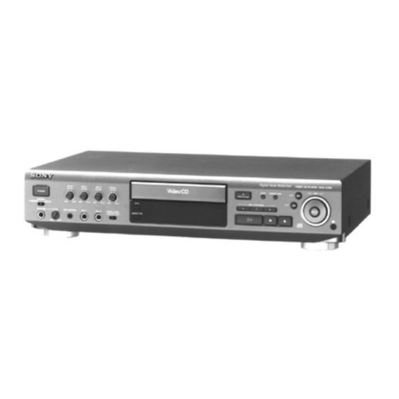
All manuals and user guides at all-guides.com SECTION 3 This section is extracted from instruction manual. GENERAL Location of Parts and Controls Front Panel 2 3 4 5 !º !¡ !™!£ !¢ !∞ #º @ª @• @¶ @§ @∞ @¢ @£... -
Page 7: Printed Wiring Board - Bd Section
All manuals and user guides at all-guides.com — 7 —... - Page 8 All manuals and user guides at all-guides.com — 8 —...
-
Page 9: Schematic Diagram - Bd Section
All manuals and user guides at all-guides.com — 9 —... - Page 10 All manuals and user guides at all-guides.com — 10 —...
- Page 11 All manuals and user guides at all-guides.com — 11 —...
-
Page 12: Printed Wiring Board - Main, Displ Section
All manuals and user guides at all-guides.com — 12 —... - Page 13 All manuals and user guides at all-guides.com — 13 —...
- Page 14 All manuals and user guides at all-guides.com — 14 —...
-
Page 15: Schematic Diagram - Main, Disp Section
All manuals and user guides at all-guides.com — 15 —... - Page 16 All manuals and user guides at all-guides.com — 16 —...
-
Page 17: Disassembly
All manuals and user guides at all-guides.com SECTION 4 DISASSEMBLY Note: Follow the disassembly procedure in the numerical order given. 4-1. FRONT PANEL • In order to remove the front panel block when the power supply does not turn on, rotate the cam with tapering driver as the figure shows, and the disc table will be moved. -
Page 18: Electrical Adjustments
All manuals and user guides at all-guides.com SECTION 5 ELECTRICAL ADJUSTMENTS CD SECTION Note : A clear RF signal waveform means that the shape “◊” can be clearly distinguished at the center of the waveform. NOTE : RF signal waveform 1. - Page 19 All manuals and user guides at all-guides.com RF PLL Free-run Frequency Check VIDEO SECTION Procedure : 1. Connect frequency counter to TP (PLCK) with lead wire. Frequency adjustment frequency counter 1. Connect the frequency counter to check point of the VIDEO board. BD board frequency counter TP (PLCK)
-
Page 20: Diagrams
All manuals and user guides at all-guides.com SECTION 6 DIAGRAMS 6-1. CIRCUIT BOARDS LOCATION TRANS board BD board VOL board PW board TR board REG board VIDEO board MIC board LOADING board MAIN board DISP board JOG board — 20 —... -
Page 21: Schematic Diagram - Video Section
All manuals and user guides at all-guides.com... - Page 22 All manuals and user guides at all-guides.com...
- Page 23 All manuals and user guides at all-guides.com...
- Page 24 All manuals and user guides at all-guides.com...
-
Page 25: Printed Wiring Board - Video Section
All manuals and user guides at all-guides.com... - Page 26 All manuals and user guides at all-guides.com...
- Page 27 All manuals and user guides at all-guides.com...
-
Page 28: Ic Block Diagrams
All manuals and user guides at all-guides.com 6-9. IC BLOCK DIAGRAMS – BD SECTION – IC101 CXD2545Q 67 62 63 64 20 19 32K RAM CLOCK GENERATOR C16M 43 PSSL ADDRESS PRIORITY VCO1 DIGITAL SERIAL GENERATOR ENCODER VCO0 PARALLEL DEMODULATOR VARI-PITCH 61-46 DA01-16... -
Page 29: Main, Disp Section
All manuals and user guides at all-guides.com – MAIN, DISP SECTION – IC104 CXD2721Q 78 77 76 75 74 73 72 71 70 69 68 67 66 65 64 63 62 61 60 59 58 57 56 55 54 53 52 51 N.C 81 AVD1 N.C 82... -
Page 30: Video Section
All manuals and user guides at all-guides.com – VIDEO SECTION – IC502 CXD1852Q 90 89 88 87 86 85 84 83 82 81 80 79 78 77 76 75 74 73 72 71 70 69 68 67 66 65 64 63 62 61 60 VDD VIDEO POSTPROCESSOR HSYNC... - Page 31 All manuals and user guides at all-guides.com IC510 MSM518126-50JSDR1 MEMORY CELL OUTPUT (1.048.576bit) BUFFER SENSE/ REFRESH AMP INPUT/OUTPUT CONTROL ROW DECODER INPUT BUFFER CLOCK GENERATOR IC511 CXD1913Q 50 49 48 46 45 44 43 42 41 40 37-39 36 35 34 33 XTEST4 BURST FLAG CSYNC...
- Page 32 All manuals and user guides at all-guides.com IC801 LC74760M-9077 28 27 26 25 24 23 21 20 19 18 17 16 CHARACTER OUTPUT SYNC SYNC SHIFT FONT DISPLAY /BACKGROUND DECODER DISCRIMINATION CIRCUIT REGISTER /VIDEO OUTPUT CONTROL DECODER CHARACTER CONTROL CONTROL COUNTER COUNTER COMPOSITE...
-
Page 33: Ic Pin Functions
All manuals and user guides at all-guides.com 6-10. IC PIN FUNCTIONS • IC101 DIGITAL SIGNAL PROCESSOR (CXD2545Q)/BD board Pin No. Pin Name Function SRON Sled drive output (Not used) SRDR Sled drive output SFON Sled drive output (Not used) TFDR Tracking drive output TRON Tracking drive output (Not used) - Page 34 All manuals and user guides at all-guides.com Pin No. Pin Name Function – Digital power supply ASYE Asymmetry circuit ON/OFF PSSL Audio data output mode selection input WDCK 48-bit slot D/A interface. Word clock. LRCK 48-bit slot D/A interface. LR clock. DATA DA 16 output when PSSL=1.
- Page 35 All manuals and user guides at all-guides.com Pin No. Pin Name Function XRST System reset DIRC Used in 1-track jump mode (+5v) SCLK SENS serial data read-out clock DFSW Defect selection pin (Ground) ATSK Input pin for anti-shock (Ground) DATA Serial data input, supplied from CPU XLAT Latch input, supplied from CPU...
-
Page 36: Ic104 Digital Signal Processor For Karaoke (Cxd2721Q)/Main Board
All manuals and user guides at all-guides.com • IC104 DIGITAL SIGNAL PROCESSOR FOR KARAOKE (CXD2721Q)/MAIN board Pin No. Pin Name Function Latch input from system controller (CXP82532-010Q) – Normally open RVDT Data input from system controller (CXP82532-010Q) – Normally open AVD0 –... - Page 37 All manuals and user guides at all-guides.com Pin No. Pin Name Function AVD4 – Power supply for CH-1 • DA converter – Normally open AVS4 – Ground for CH-1 • DA converter – Normally open AOUT1 CH-1 • DA converter • LPF output (Not used. open) AVS1 –...
-
Page 38: Ic402 System Control, Fl Driver (Cxp82532-010Q)/Disp Board
All manuals and user guides at all-guides.com • IC402 SYSTEM CONTROL, FL DRIVER (CXP82532-010Q)/DISP board Pin No. Pin Name Function TEST2 Test mode 2. Normally “H”. RM IN Remote commander signal input Jog shuttle input B JOG-1B Not used (Inhibit use. Keep the pin open.) 4 to 5 ——... -
Page 39: Ic501 Mechanism Control (Hd6433032Sk07F)/Video Board
All manuals and user guides at all-guides.com • IC501 MECHANISM CONTROL (HD6433032SK07F)/VIDEO board Pin No. Pin Name Function CMD0 Input/output terminal exchanging data bus 0 with system controller CMD1 Input/output terminal exchanging data bus 1 with system controller CMD2 Input/output terminal exchanging data bus 2 with system controller CMD3 Input/output terminal exchanging data bus 3 with system controller SACK... - Page 40 All manuals and user guides at all-guides.com Pin No. Pin Name Function Address bus output MPEG MPEG wait input Operation mode setting terminal (Connected to +5V) Operation mode setting terminal (Connected to ground) φ System clock output (Not used) Shifts to the hardware standby mode when the standby terminal becomes “Low”. STBY (Unable to use H level fixed) (Connected to +5V) RESET...
-
Page 41: Ic507 Mpeg Decoder (Cxd1852Q)/Video Board
All manuals and user guides at all-guides.com • IC507 MPEG DECODER (CXD1852Q)/VIDEO board Pin No. Pin Name Function – Ground Video decoder master clock pin. Input the XTL0I clock or connect an oscillator between XTL0O XTL0I and XTL0O. The recommended frequencies are 27MHz, 28.6363MHz (NTSC 8fsc), and 35.4686 MHz (PAL 8fsc). - Page 42 All manuals and user guides at all-guides.com Pin No. Pin Name Function Data input/output signal pin. Connect to the DRAM data pin so that the lower and upper bytes of the data correspond to the CAS0 to CAS3 controls. MD10 –...
- Page 43 All manuals and user guides at all-guides.com Pin No. Pin Name Function B/Cb0 B/Cb1 B/Cb2 B/Cb3 Output pin of the B or Cb signal of the image data. MSB is B/Cb7. Synchronizes with B/Cb4 DCLK. B/Cb5 B/Cb6 B/Cb7 Dot clock (DCLK) signal pin. The DCLK frequency is normally 13.5MHz. The DCLK can DCLK be input from this pin or can be made by frequency-dividing (1/integer) the clock input from XTL0I.
- Page 44 All manuals and user guides at all-guides.com Pin No. Pin Name Function DATI Serial data input BCKI Bit clock input DOIN Digital input signal XHCS Register access chip select signal pin. Data acknowledge/wait signal pin for DMA transmission, register access, transparent XHDT memory access.
-
Page 45: Ic509 Video Picture Quality Improvement (Cxd1853Q)/Video Board
All manuals and user guides at all-guides.com • IC509 VIDEO PICTURE QUALITY IMPROVEMENT (CXD1853Q)/VIDEO board Pin No. Pin Name Function – Ground [MSB] B input 0-7 (Connect to ground) [LSB] – Ground Y/GI7 [MSB] Y/GI6 Y/GI5 Y/GI4 G (Y) input 0-7 Y/GI3 Y/GI2 Y/GI1... - Page 46 All manuals and user guides at all-guides.com Pin No. Pin Name Function – Ground DIO3 DIO2 DIO1 DIO0 DRAM data I/O 0-7 DIO4 DIO5 DIO6 DIO7 – Ground C/RO0 [MSB] C/RO1 C/RO2 C/RO3 R (Cb/Cr) output 0-7 C/RO4 C/RO5 C/RO6 C/RO7 [LSB] –...
- Page 47 All manuals and user guides at all-guides.com Pin No. Pin Name Function CSYNC.O Composit SYNC output – Ground TEST 0 For test (Connect to ground) TEST 1 TEST 2 For test TEST 3 For test (Connect to ground) IFSEL 1 Matrix select RGB/XYC (Connect to ground) IFSEL 2 System select D1851/XD1852 (Connect to ground)
-
Page 48: Ic511 Digital Video Encoder (Cxd1913Q)/Video Board
All manuals and user guides at all-guides.com • IC511 DIGITAL VIDEO ENCODER (CXD1913Q)/VIDEO board Pin No. Pin Name Function 8-bit pixel data input pins (PD0 to 7). When control register bit “PIF MODE”=”0", serve as input pins for multiplexed Y, Cb, Cr signals. - Page 49 – The functions of this pin are selected by Pin 64 XIICEN. When the XIICEN pin is “H”, sets into the SONY SIO mode, and becomes the SI serial data input pin. When the XIICEN pin is “L”, sets into the I C-BUS mode, and becomes the SDA input/ output pin.
- Page 50 H.sync signal output The functions of this pin are selected by Pin 64 XIICEN. When the XIICEN pin is “H”, sets into the SONY SIO mode, and becomes the S0 serial- out output pin. When the XIICEN pin is “L”, this pin is not used and sets into high impedance.
-
Page 51: Ic801 Character Generator (Lc74760)/Video Board
All manuals and user guides at all-guides.com • IC801 CHARACTER GENERATOR (LC74760)/VIDEO board Pin No. Pin Name Function – Ground connect pin Pin for connecting to the capacitor or crystal of oscillator for internal sync signal oscilla- XTAL IN1 tion applications (Crystal oscilloation for NTSC: 4fsc=14.318MHz) Pin for connecting to the capacitor or crystal of oscillator for internal sync signal oscilla- XTAL OUT1 tion applications (Crystal oscilloation for NTSC: 4fsc=14.318MHz). -
Page 52: Exploded Views
4-984-999-01 PANEL, LOADING * 16 1-664-225-11 PW BOARD X-4947-889-1 PANEL ASSY, FRONT * 17 A-4699-498-A DISP BOARD, COMPLETE 4-963-404-21 EMBLEM (5-A), SONY * 18 4-932-810-11 CUSHION (FL) 4-984-893-22 PLATE (FL), INDICATION * 19 4-961-264-01 HOLDER (FL TUBE 3.5) 4-984-895-01 PLATE, INDICATON 4-988-408-21 BUTTON (SELECT) 4-981-435-01 RING (DIA. -
Page 53: Chassis Section
All manuals and user guides at all-guides.com 7-2. CHASSIS SECTION CNP901 CDM14-5BD21 F901 T901 not supplied supplied not supplied not supplied The components identified by mark ! or dotted line with mark ! are critical for safety. Replace only with part number specified. -
Page 54: Mechanism Deck Section (Cdm14-5Bd21)
All manuals and user guides at all-guides.com 7-3. MECHANISM DECK SECTION (CDM14-5BD21) BU-5BD21 not supplied not supplied M151 Ref. No. Part No. Description Remark Ref. No. Part No. Description Remark 1-452-538-11 MAGNET 4-933-134-01 SCREW (+PTPWH M2.6X6) 4-933-110-41 HOLDER (MG) 4-933-112-01 TABLE, DISC 4-959-996-01 SPRING (932), COMPRESSION 4-967-268-01 GEAR (C) 4-933-129-01 HOLDER (BU) -
Page 55: Base Unit Section (Bu-5Bd21)
All manuals and user guides at all-guides.com 7-4. BASE UNIT SECTION (BU-5BD21) M102 M101 (including r A) The components identified by mark ! or dotted line with mark ! are critical for safety. Replace only with part number specified. Ref. No. Part No. -
Page 56: Electrical Parts List
All manuals and user guides at all-guides.com SECTION 8 ELECTRICAL PARTS LIST Note: • SEMICONDUCTORS • Due to standardization, replacements in the parts list The components identified by In each case, u: µ , for example: may be different from the parts specified in the mark ! or dotted line with mark ! uA...: µ... - Page 57 All manuals and user guides at all-guides.com DISP Ref. No. Part No. Description Remark Ref. No. Part No. Description Remark R160 1-216-295-91 CONDUCTOR, CHIP (2012) < TRANSISTOR > R161 1-216-308-00 METAL CHIP 1/10W Q401 8-729-900-80 TRANSISTOR DTC114ES R162 1-216-101-00 METAL CHIP 150K 1/10W Q402...
- Page 58 All manuals and user guides at all-guides.com LOADING MAIN DISP Ref. No. Part No. Description Remark Ref. No. Part No. Description Remark R450 1-249-411-11 CARBON 1/4W < MOTOR > R451 1-249-411-11 CARBON 1/4W R452 1-249-411-11 CARBON 1/4W M151 A-4604-363-A MOTOR (L) ASSY (LOADING) R453 1-249-411-11 CARBON 1/4W...
- Page 59 All manuals and user guides at all-guides.com MAIN Ref. No. Part No. Description Remark Ref. No. Part No. Description Remark C145 1-137-360-11 FILM 220PF < DIODE > C146 1-124-748-11 ELECT 22uF 100V C147 1-126-024-11 ELECT 220uF D101 8-719-200-82 DIODE 11ES2 C152 1-126-960-11 ELECT D301...
- Page 60 All manuals and user guides at all-guides.com MAIN Ref. No. Part No. Description Remark Ref. No. Part No. Description Remark < RESISTOR > R153 1-259-460-11 CARBON 1/6W R154 1-259-460-11 CARBON 1/6W R101 1-249-429-11 CARBON 1/4W R156 1-259-466-11 CARBON 1/6W R102 1-249-433-11 CARBON 1/4W R157...
- Page 61 All manuals and user guides at all-guides.com MAIN Ref. No. Part No. Description Remark Ref. No. Part No. Description Remark R320 1-249-417-11 CARBON 1/4W F D706 8-719-987-63 DIODE 1N4148M < SWITCH > < GROUND TERMINAL > S301 1-571-552-11 SWITCH, SLIDE (COLOR SYSTEM) EB701 1-537-770-21 TERMINAL BOARD, GROUND <...
- Page 62 All manuals and user guides at all-guides.com TRANS Ref. No. Part No. Description Remark Ref. No. Part No. Description Remark R724 1-259-428-11 CARBON 1/6W 1-664-222-11 TR BOARD R725 1-259-428-11 CARBON 1/6W ********* R727 1-259-448-11 CARBON 6.8K 1/6W < TRANSISTOR > R728 1-259-448-11 CARBON 6.8K...
- Page 63 All manuals and user guides at all-guides.com TRANS VIDEO Ref. No. Part No. Description Remark Ref. No. Part No. Description Remark < TRANSFORMER > C570 1-163-231-11 CERAMIC CHIP 15PF C571 1-163-038-91 CERAMIC CHIP 0.1uF ! T901 1-431-083-11 TRANSFORMER, POWER C583 1-163-038-91 CERAMIC CHIP 0.1uF C584...
- Page 64 All manuals and user guides at all-guides.com VIDEO Ref. No. Part No. Description Remark Ref. No. Part No. Description Remark < CONNECTOR > R505 1-216-025-91 METAL GLAZE 1/10W CN501 1-766-942-11 CONNECTOR, FFC/FPC 29P R506 1-216-025-91 METAL GLAZE 1/10W * CN502 1-770-154-11 PIN, CONNECTOR (PC BOARD) 6P R507 1-216-025-91 METAL GLAZE...
- Page 65 All manuals and user guides at all-guides.com VIDEO Ref. No. Part No. Description Remark Ref. No. Part No. Description Remark R563 1-216-025-91 METAL GLAZE 1/10W < VARIABLE RESISTOR > R564 1-216-025-91 METAL GLAZE 1/10W R565 1-216-025-91 METAL GLAZE 1/10W RV702 1-225-407-11 RES, VAR 50K (VOCAL LEVEL) R567 1-216-047-91 METAL GLAZE...
- Page 66 All manuals and user guides at all-guides.com MCE-K700 Sony Corporation 96K097012-1 Printed in Singapore © 1996. 11 9-960-824-11 Home A&V Products Company Published by Service and Safety Engineering Dept. (Shibaura) — 88 —...