Table of Contents
Advertisement
Quick Links
SERVICE MANUAL
Ver 1.0 2001.06
MCE-SV7 is the Video CD/CD player
section in MHC-SV7AV.
Sony Corporation
9-873-155-01
2001F0500-1
Home Audio Company
C 2001.6
Shinagawa Tec Service Manual Production Group
Model Name Using Similar Mechanism
CD Mechanism Type
Base Unit Name
Optical Pick-up Name
SPECIFICATIONS
VIDEO CD/CD player section
System
Compact disc and digital
audio system
Laser
Semiconductor laser
(λ=795 nm)
Emission duration:
continuous
Frequency response
2 Hz – 20 kHz (±0.5 dB)
Signal-to-noise ratio
More than 90 dB
Dynamic range
More than 90 dB
Video color system format
NTSC, PAL
OPTICAL OUT
(Square optical connector jack, rear panel)
General
Dimensions (w/h/d)
Approx. 280 x 108 x 330 mm
Mass
Approx. 2.8 kg
Design and specifications are subject to change
without notice.
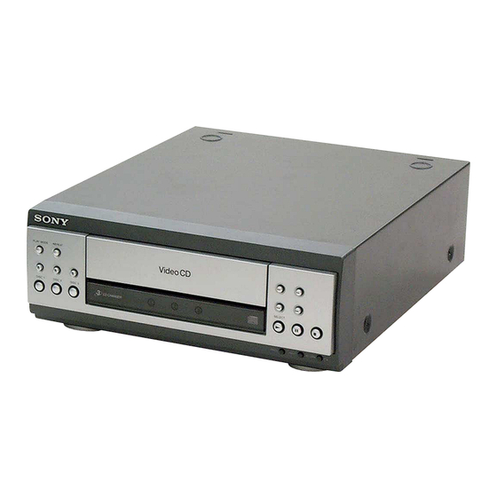
MCE-SV7
VIDEO CD/CD PLAYER
E Model
NEW
CDM63B
BU-30BD61A
OP Assy (A-MAX.3)
Advertisement
Table of Contents

Related Manuals for Sony MCE-SV7


Summary of Contents for Sony MCE-SV7
- Page 1 MCE-SV7 SERVICE MANUAL E Model Ver 1.0 2001.06 MCE-SV7 is the Video CD/CD player section in MHC-SV7AV. Model Name Using Similar Mechanism CD Mechanism Type CDM63B Base Unit Name BU-30BD61A Optical Pick-up Name OP Assy (A-MAX.3) SPECIFICATIONS VIDEO CD/CD player section...
- Page 2 LINE WITH MARK 0 ON THE SCHEMATIC DIAGRAMS AND IN THE PARTS LIST ARE CRITICAL TO SAFE OPERATION. REPLACE THESE COMPONENTS WITH SONY PARTS WHOSE PART NUMBERS APPEAR AS SHOWN IN THIS MANUAL OR IN SUPPLEMENTS PUB- LISHED BY SONY.
-
Page 3: Table Of Contents
MCE-SV7 TABLE OF CONTENTS SERVICING NOTES ..........4 GENERAL ..............5 DISASSEMBLY 3-1. Disassembly Flow ............6 3-2. Cover ................7 3-3. CD Mechanism Deck (CDM63B) ........7 3-4. MAIN Board ..............8 3-5. Front Panel Section ............8 3-6. PANEL Board, SUB PANEL Board ....... 9 3-7. -
Page 4: Servicing Notes
MCE-SV7 SECTION 1 SERVICING NOTES This set is a component of the MHC-SV7AV. CD-TEXT TEST DISC The MHC-SV7AV system configuration is as shown below, and therefore it does not operate normally unless all four components This unit is able to display the test data (character information) are connected. -
Page 5: General
MCE-SV7 SECTION 2 This section is extracted from instruction manual. GENERAL Parts Identification The items are arranged in alphabetical order. Refer to the pages indicated in parentheses ( ) for details. Main unit Remote Control VIDEO CD/CD player CHECK qd (17) -
Page 6: Disassembly
MCE-SV7 SECTION 3 DISASSEMBLY • This set can be disassembled in the order shown below. 3-1. DISASSEMBLY FLOW 3-2. COVER (Page 7) 3-3. CD MECHANISM DECK 3-5. FRONT PANEL SECTION 3-4. MAIN BOARD (CDM63B) (Page 8) (Page 8) (Page 7) 3-6. -
Page 7: Cover
MCE-SV7 Note: Follow the disassembly procedure in the numerical order given. 3-2. COVER 2 screw 3 cover (BVTT3 × 6) 1 two screws (case 3 TP2) 1 two screws (case 3 TP2) 3-3. CD MECHANISM DECK (CDM63B) 4 CD mechanism deck... -
Page 8: Main Board
MCE-SV7 3-4. MAIN BOARD 2 two connectors (CN101, 102) 5 MAIN board 1 wire (flat type) (13 core) (CN301) 3 screw 2 connector (BVTP3 × 8) (CN401) 3 two screws (BVTP3 × 8) 4 lug 3 screw (BVTP3 × 8) -
Page 9: Panel Board, Sub Panel Board
MCE-SV7 3-6. PANEL BOARD, SUB PANEL BOARD 4 four screws (BVTP2.6 × 8) 6 SUB PANEL board 5 two claws 1 five screws (BVTP2.6 × 8) 3 PANEL board 2 two claws 3-7. LID (CD) 2 bracket (LID) assy 1 screw (BVTP2.6 ×... -
Page 10: Test Mode
TEST MODE Note: Use following buttons in the test mode. [CD Service Mode] no mark : Button of video CD unit (MCE-SV7) • This mode can run the CD sled motor optionally. Use this mode, : Button of amplifier unit (TA-SV7AV) for instance, when cleaning the optical pick-up. -
Page 11: Electrical Adjustments
MCE-SV7 SECTION 5 ELECTRICAL ADJUSTMENTS Note: Clear RF signal waveform means that the shape “◊” can be Checking Location : CD SECTION VIDEO SECTION clearly distinguished at the center of the waveform. Note : Video Frequency Adjustment [ BD BOARD ] — SIDE B —... -
Page 12: Diagrams
MCE-SV7 SECTION 6 DIAGRAMS 6-1. BLOCK DIAGRAM – CD SERVO Section – FILTER XTSL RF AMP, DIGITAL SIGNAL PROCESSOR FOCUS/TRACKING ERROR AMP IC101 (1/2) 53 55 52 54 XTAO IC103 DETECTOR CD +5V MCLK CLOCK 33.8MHz XTAI GENERATOR BUFFER (Page 13) -
Page 13: Block Diagram - Audio/Video Section
MCE-SV7 6-2. BLOCK DIAGRAM – AUDIO/VIDEO Section – DIGITAL FILTER, D/A CONVERTER IC509 MCLK 33.8MHz CN102 (1/2) (Page 12) MPEG VIDEO/AUDIO DECODER, DIGITAL DATA DA-DATA VOUTL VCD L-IN VIDEO SIGNAL PROCESSOR MPEG AUDIO INPUT FILTER, LOW-PASS SYSTEM DA-BCK LOW-PASS IC505... -
Page 14: Block Diagram - Main Section
MCE-SV7 6-3. BLOCK DIAGRAM – MAIN Section – SYSTEM CONTROLLER IC401 CN103 S701 – 708, DATA-OUT DATA-OUT S711 – 720 EXP-OUT DATA DATA-OUT DATA-IN EXP-IN DATA DATA-IN DATA-IN EXP-CLK EXP-LAT KEY2 KEY2 (TC) KEY2 KEY2 ATRIG A-TRIG BTRIG SYSTEM CONTROL 5... -
Page 15: Note For Printed Wiring Boards And Schematic Diagrams
MCE-SV7 6-4. NOTE FOR PRINTED WIRING BOARDS AND SCHEMATIC DIAGRAMS • Circuit Boards Location (In addition to this, the necessary note is printed in each block) Note on Schematic Diagram: Note on Printed Wiring Boards: • All capacitors are in µF unless otherwise noted. pF: µµF •... -
Page 16: Printed Wiring Board - Bd Section
MCE-SV7 6-5. PRINTED WIRING BOARD – BD Section – • See page 15 for Circuit Boards Location. IC102 TP (DVC) TP (FEI) TP (FEO) IC104 TP (TEO) IC101 TP (RFDC) TP (XPCK) IC103 BOARD CN501 (Page 20) (VC) IC106 • Semiconductor Location (A-MAX.3) -
Page 17: Schematic Diagram - Bd Section
MCE-SV7 6-6. SCHEMATIC DIAGRAM – BD Section – • • See page 28 for Waveforms. See page 29 for IC Block Diagrams. TP (RFAC) (FEI) IC 106 TP (RFDC) Q101 2SB710A OSC BUFFER (VC) (TEO) (FEO) TP (DVC) RF AMP,... -
Page 18: Cd Changer Section
MCE-SV7 6-7. PRINTED WIRING BOARDS – CD CHANGER Section – • See page 15 for Circuit Boards Location. MAIN BOARD NO202 (Page 24) -
Page 19: Schematic Diagram - Cd Changer Section
MCE-SV7 6-8. SCHEMATIC DIAGRAM – CD CHANGER Section – • See page 29 for IC Block Diagram. IC731 SUB TRAY1 HEIGHT SENSOR IC732 SUB TRAY2 HEIGHT SENSOR IC733 SUB TRAY3 HEIGHT SENSOR MAIN BOARD NO202 (Page 25) IC751 DISC IN DETECT •... -
Page 20: Printed Wiring Boards
MCE-SV7 6-9. PRINTED WIRING BOARDS – AUDIO/VIDEO Section – • See page 15 for Circuit Boards Location. VIDEO BOARD VMP BOARD VMP BOARD (SIDE A) (SIDE B) NO801 J801 IC304 S VIDEO OUT CN302 IC302 C801 (CHASSIS) CLP801 (CHASSIS) J802... -
Page 21: Schematic Diagram - Audio/Video Section (1/3)
MCE-SV7 6-10. SCHEMATIC DIAGRAM – AUDIO/VIDEO Section (1/3) – • See page 28 for Waveform. LEVEL SHIFT CL680 RESET VIDEO CD CONTROLLER IC502 M30622MGA-A59FP BD BOARD CN101 (Page 17) BOARD (3/3) (Page 23) MAIN BOARD CN301 (Page 25) VMP BOARD... -
Page 22: Schematic Diagram - Audio/Video Section (2/3)
MCE-SV7 6-11. SCHEMATIC DIAGRAM – AUDIO/VIDEO Section (2/3) – • See page 28 for Waveforms. (Page 21) VMP BOARD (1/3) Q502 BOARD DTC114EKA- (3/3) T146 BUFFER (Page 23) D-RAM Q531 2SD999-T1- CLCK +3.3V REGULATOR Q501 DTC114EKA- T146 BUFFER VIDEO SIGNAL PROCESSOR... -
Page 23: Schematic Diagram - Audio/Video Section (3/3)
MCE-SV7 6-12. SCHEMATIC DIAGRAM – AUDIO/VIDEO Section (3/3) – • • See page 28 for Waveforms. See page 29 for IC Block Diagrams. VIDEO J802 VIDEO OUT CN302 NO801 J801 S VIDEO OUT CLP801 (CHASSIS) C801 0.1 C802 0.1 (CHASSIS) -
Page 24: Printed Wiring Boards - Main Section
MCE-SV7 6-13. PRINTED WIRING BOARDS – MAIN Section – • See page 15 for Circuit Boards Location. (Page 20) (Page 18) SYSTEM CONTROL 3 VMP BOARD DRIVER BOARD TO ST-SV7 CN502 CN701 MAIN BOARD (CHASSIS) SYSTEM CONTROL 5 TO TC-S3... -
Page 25: Schematic Diagram - Main Section
MCE-SV7 6-14. SCHEMATIC DIAGRAM – MAIN Section – • See page 28 for Waveform. OPTICAL OUT TO ST-SV7 CLP102 C122 C103 CN301 IC102 0.022 0.022 TOTX140 I2C.DATA VCD401 C102 C101 C125 OPTICAL (CHASSIS) I2C.CLK VCD402 D502 D501 TRANSCEIVER 21DQ04 21DQ04... -
Page 26: Printed Wiring Boards - Panel Section
MCE-SV7 6-15. PRINTED WIRING BOARDS – PANEL Section – • See page 15 for Circuit Boards Location. (Page 24) PANEL BOARD SUB PANEL BOARD REPEAT PLAY MODE > (DISC 3) (DISC 2) (DISC 1) DISC 3 DISC 2 DISC 1... -
Page 27: Schematic Diagram - Panel Section
MCE-SV7 6-16. SCHEMATIC DIAGRAM – PANEL Section – R707 R706 R705 R704 R703 R702 R701 R700 1.8k 1.2k CN701 S708 S707 S706 S705 S704 S703 S702 S701 PLAY MODE REPEAT DISC 1 DISC 2 DISC 3 (DISC 3) (DISC 2) - Page 28 MCE-SV7 • Waveforms – BD Board – – VMP Board – – MAIN Board – 1 IC101 t; (RFAC) (CD Play mode) 1 IC502 qd (XOUT) 6 IC505 <z/,> (DA-LRCK) qa J801 4 (YOUT) qa IC401 qd (X-OUT) 1.3 Vp-p 2.0 Vp-p...
- Page 29 MCE-SV7 • IC Block Diagrams – BD Board – IC101 CXD3068Q 59 58 57 56 55 54 53 52 51 50 49 48 47 46 45 44 43 42 41 DVDD2 ASYE DIGITAL ASYMMETRY CORRECTOR DIGITAL DOUT LRCK D/A DIGITAL...
- Page 30 MCE-SV7 – DRIVER Board – IC103 CXA2581N-T4 IC701 BA6956AN RW/ROM DC OFST RFDCI – – RFDCO CONTROL LOGIC – RW/ROM VOFST APC AMP EQ ON/OFF RFAC EQ IN RW/ROM RFAC AC SUM SUMMING VOFST – – RW/ROM TE BAL RW/ROM –...
- Page 31 MCE-SV7 – VMP Board – IC302 NJM2255M (TE2) IC303 NJM2209M (TE2) SATURATION +Ø ADJUST (COLOR BURST) HUE ADJUST SECONDARY LOWER CLAMP SATURATION DIFFERENTIATION LIMITER SYNC ADJUST GAIN ADJ CHIP –X (COLOR BURST) SWITCH CONTROL LOWER LIMITER IC304 BA7665FS-E2 IC509 PCM1727E-2/T2...
-
Page 32: Ic Pin Function Description
MCE-SV7 6-17. IC PIN FUNCTION DESCRIPTION • BD BOARD IC101 CXD3068Q (DIGITAL SIGNAL PROCESSOR, DIGITAL SERVO PROCESSOR) Pin No. Pin Name Description DVDD0 — Power supply terminal (+3.3V) (digital system) XRST Reset signal input from the video CD controller (IC502) “L”: reset MUTING Muting on/off control signal input from the video CD controller (IC502) “H”: muting on... - Page 33 MCE-SV7 Pin No. Pin Name Description AVSS0 — Ground terminal (analog system) IGEN Stabilized current input for operational amplifiers AVDD0 — Power supply terminal (+3.3V) (analog system) ASYO EFM full-swing output terminal ASYI Asymmetry comparator voltage input terminal RFAC EFM signal input from the CXA2581N (IC103) AVSS1 —...
- Page 34 MCE-SV7 • VMP BOARD IC502 M30622MGA-A59FP (VIDEO CD CONTROLLER) Pin No. Pin Name Description SENSE Internal status (SENSE) signal input from the CXD3068Q (IC101) SENSE CLK Sense serial data reading clock signal output to the CXD3068Q (IC101) RESOLUTION Serial data output to the Y amplifier (IC303)
- Page 35 MCE-SV7 Pin No. Pin Name Description BUS XWRL Not used LO.BOOST Low boost control signal output terminal Not used (open) AUDIO MUTING Audio muting on/off control signal output terminal “L”: muting on Not used (open) LOAD OUT Loading motor drive signal output terminal Not used (open)
- Page 36 MCE-SV7 • VMP BOARD IC505 CL680T-D1 (MPEG VIDEO/AUDIO DECODER, VIDEO SIGNAL PROCESSOR) Pin No. Pin Name Description Not used (open) — Ground terminal CD-BCK CD decode bit clock signal (2.8224 MHz) input from the CXD3068Q (IC101) CD-DATA CD decode data input from the CXD3068Q (IC101) CD-LRCK CD decode L/R sampling clock signal (44.1 kHz) input from the CXD3068Q (IC101)
- Page 37 MCE-SV7 Pin No. Pin Name Description AGND-DAC — Ground terminal (for D/A converter) RREF Fix the video signal output level control VREF Reference voltage (+1.235V) output terminal AVDD-DAC — Power supply terminal (+3.3V) (for D/A converter) C-OUT Chrominance video signal output terminal AGND-DAC —...
- Page 38 MCE-SV7 Pin No. Pin Name Description HSEL Command selection signal input from the video CD controller (IC502) CDG-SDATA Not used (fixed at “L”) CDG-VFSY Not used (fixed at “L”) CDG-S0S1 Not used (fixed at “L”) 125 to 128 Not used (open)
- Page 39 MCE-SV7 • MAIN BOARD IC401 M30620MAA-B53FP (SYSTEM CONTROLLER) Pin No. Pin Name Description 1 to 7 — — Not used (open) External data bus line byte selection signal input “L”: 16 bits, “H”: 8 bits BYTE Not used (fixed at “L”) CNVSS —...
- Page 40 MCE-SV7 Pin No. Pin Name Description Detection input from the disc tray 3 height sensor (IC733) T-SENS3 “H”: disc tray 3 position is chucking position — — Not used (fixed at “H”) DISC-SENS Detection input from the disc in detect sensor (IC751)
-
Page 41: Exploded Views
MCE-SV7 SECTION 7 EXPLODED VIEWS NOTE: • -XX and -X mean standardized parts, so they • Items marked “*” are not stocked since they The components identified by mark 0 or dotted line with mark may have some difference from the original are seldom required for routine service. -
Page 42: Chassis Section
MCE-SV7 7-2. CHASSIS SECTION CDM63B BU-30BD61A not supplied not supplied not supplied not supplied not supplied not supplied Ref. No. Part No. Description Remark Ref. No. Part No. Description Remark 4-951-620-01 SCREW (2.6X8), +BVTP 1-769-977-11 WIRE (FLAT TYPE) (13 CORE) -
Page 43: Cd Mechanism Deck Section-1 (Cdm63B)
MCE-SV7 7-3. CD MECHANISM DECK SECTION-1 (CDM63B) not supplied not supplied not supplied not supplied supplied not supplied not supplied not supplied not supplied not supplied not supplied Ref. No. Part No. Description Remark Ref. No. Part No. Description Remark 4-218-253-01 SCREW (M2.6), +BTTP... -
Page 44: Cd Mechanism Deck Section-2 (Cdm63B)
MCE-SV7 7-4. CD MECHANISM DECK SECTION-2 (CDM63B) not supplied not supplied not supplied M721 Ref. No. Part No. Description Remark Ref. No. Part No. Description Remark 4-985-672-01 SCREW (+PTPWH M2.6), FLOATING 4-228-998-01 GEAR (DETECTION) 4-229-002-02 GEAR (SLIDER) 4-228-976-01 SLIDER (BU. R) 4-218-254-21 SCREW (M2.6), +PTPWH... -
Page 45: Base Unit Section (Bu-30Bd61A)
MCE-SV7 7-5. BASE UNIT SECTION (BU-30BD61A) The components identified by mark 0 or dotted line with mark 0 are critical for safety. Replace only with part number specified. Ref. No. Part No. Description Remark Ref. No. Part No. Description Remark... -
Page 46: Electrical Parts List
MCE-SV7 SECTION 8 ELECTRICAL PARTS LIST NOTE: • Due to standardization, replacements in the • Items marked “*” are not stocked since they The components identified by mark 0 or dotted line with mark parts list may be different from the parts speci- are seldom required for routine service. - Page 47 MCE-SV7 DISC SENSOR DRIVER IN OUT SW MAIN Ref. No. Part No. Description Remark Ref. No. Part No. Description Remark R151 1-216-097-11 RES-CHIP 100K 1/10W 1-678-460-11 DRIVER BOARD R152 1-216-065-00 RES-CHIP 4.7K 1/10W ************* R163 1-216-295-11 SHORT R164 1-216-295-11 SHORT <...
- Page 48 MCE-SV7 MAIN Ref. No. Part No. Description Remark Ref. No. Part No. Description Remark < IC > C311 1-162-306-11 CERAMIC 0.01uF C312 1-161-494-00 CERAMIC 0.022uF IC102 8-749-019-13 IC TOTX140 (OPTICAL OUT TO ST-SV7) C357 1-126-964-11 ELECT 10uF IC401 6-800-589-01 IC M30620MAA-B53FP...
- Page 49 MCE-SV7 MAIN MOTOR PANEL SUB PANEL TRAY SENSOR Ref. No. Part No. Description Remark Ref. No. Part No. Description Remark R486 1-247-807-31 CARBON 1/4W S719 1-771-410-21 SWITCH, TACTILE (PREV) R487 1-247-807-31 CARBON 1/4W S720 1-771-410-21 SWITCH, TACTILE (NEXT) R489 1-247-807-31 CARBON...
- Page 50 MCE-SV7 VIDEO Ref. No. Part No. Description Remark Ref. No. Part No. Description Remark 1-680-998-12 VIDEO BOARD C532 1-164-156-11 CERAMIC CHIP 0.1uF C535 1-164-156-11 CERAMIC CHIP 0.1uF ************ C536 1-126-193-11 ELECT < CAPACITOR > C537 1-126-206-11 ELECT CHIP 100uF 6.3V...
- Page 51 MCE-SV7 Ref. No. Part No. Description Remark Ref. No. Part No. Description Remark IC505 8-759-535-48 IC CL680T-D1 R501 1-216-809-11 METAL CHIP 1/16W IC507 8-759-342-01 IC MSM514260E-60JS-7R R502 1-216-809-11 METAL CHIP 1/16W IC509 8-759-535-62 IC PCM1727E-2/T2 R503 1-216-809-11 METAL CHIP 1/16W...
- Page 52 MCE-SV7 Ref. No. Part No. Description Remark Ref. No. Part No. Description Remark MISCELLANEOUS ************** 1-823-056-11 WIRE (FLAT TYPE) (25 CORE) 1-769-977-11 WIRE (FLAT TYPE) (13 CORE) 1-757-633-11 CORD (WITH CONNECTOR) 17P 1-782-817-11 WIRE (FLAT TYPE) (16 CORE) 0 603...
- Page 53 MCE-SV7 MEMO...
-
Page 54: Revision History
MCE-SV7 REVISION HISTORY Clicking the version allows you to jump to the revised page. Also, clicking the version at the upper right on the revised page allows you to jump to the next revised page. Ver. Date Description of Revision...
Need help?
Do you have a question about the MCE-SV7 and is the answer not in the manual?
Questions and answers