Table of Contents
Advertisement
Quick Links
2003 Panasonic Communications Co., Ltd. All rights reserved.
Unauthorized copying and distribution is a violation of law.
IMPORTANT INFORMATION ABOUT LEAD FREE, (PbF),
SOLDERING
If lead free solder was used in the manufacture of this product the printed circuit boards will be
marked PbF.
Standard leaded, (Pb), solder can be used as usual on boards without the PbF mark.
When this mark does appear please read and follow the special instructions described in this
manual on the use of PbF and how it might be permissible to use Pb solder during service and
repair work.
ORDER NO. KMS0306778C2
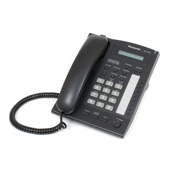
Digital Proprietary Telephone
KX-T7665NE / KX-T7665NE-B
1
White version
Black version
(for Europe)
Advertisement
Table of Contents

Related Manuals for Panasonic KX-T7665NE


Summary of Contents for Panasonic KX-T7665NE
- Page 1 KX-T7665NE / KX-T7665NE-B White version Black version (for Europe) 2003 Panasonic Communications Co., Ltd. All rights reserved. Unauthorized copying and distribution is a violation of law. IMPORTANT INFORMATION ABOUT LEAD FREE, (PbF), SOLDERING If lead free solder was used in the manufacture of this product the printed circuit boards will be marked PbF.
-
Page 2: About Lead Free Solder (Pbf: Pb Free)
1. ABOUT LEAD FREE SOLDER (PbF: Pb free) Note: In the information below, Pb, the symbol for lead in the periodic table of elements, will refer to standard solder or solder that contains lead. We will use PbF solder when discussing the lead free solder used in our manufacturing process which is made from Tin, (Sn), Silver, (Ag), and Copper, (Cu). -
Page 3: For Service Technicians
The following lead free (PbF) solder wire gauges are recommended for service of this product: 0.3mm, 0.6mm and 1.0mm. 1.2. HOW TO RECOGNIZE THAT Pb FREE SOLDER IS USED PbF is stamped to show that Pb free solder is used. (See the figure below.) 2. - Page 5 5. CONNECTION Caution: The availability of D-XDP function depends on the software version of the connected Business Telephone System. Consult your dealer for more details about D-XDP. 6. DISASSEMBLY INSTRUCTIONS...
- Page 6 1. Remove the Stand. 2. Remove 5 Screws (A). 3. Remove the Cabinet Cover.
-
Page 7: How To Replace A Flat Package Ic
4. Remove the Connector from the Main Board. 5. Remove 2 Screws (A). 6. Remove the Main Board and the LCD from the Cabinet Body. 7. HOW TO REPLACE A FLAT PACKAGE IC 7.1. PREPARATION - PbF (: Pb free) Solder - Soldering Iron Tip Temperature of 700°F ±... -
Page 8: Troubleshooting Guide
Be certain each pin is located over the correct pad on the PCB. 2. Apply flux to all of the pins on the IC. 3. Being careful to not unsolder the tack points, slide the soldering iron along the tips of the pins while feeding enough solder to the tip so that it flows under the pins as they are heated. -
Page 9: Lcd Does Not Operate
8.1. NO OPERATION Note: Refer to (1)~(4) of WAVEFORM () for waveform. 8.2. LCD DOES NOT OPERATE... -
Page 10: Handset Does Not Work
Note: Refer to (5) of WAVEFORM () for waveform. 8.3. HANDSET DOES NOT WORK Receive Send... -
Page 11: Speaker-Phone Trouble
Note: Refer to (6)~(7) of WAVEFORM () for waveform. 8.4. SPEAKER-PHONE TROUBLE Receive Send... -
Page 12: Dxdp-Dpt Does Not Work
Note: Refer to (6)~(7) of WAVEFORM () for waveform. 8.5. DXDP-DPT DOES NOT WORK Note: Refer to (8) of WAVEFORM () for waveform. 9. BLOCK DIAGRAM 10. CIRCUIT OPERATIONS 10.1. KEY INPUT CONTROL CIRCUIT The key data is under the matrix control by 20 to 23(KEYOUT) and 28 to 35(KEYIN) of IC6. The key information outputted from KEYOUT is inputted into KEYIN, when the key is pressed. -
Page 13: Lcd Control Circuit
10.2. LCD CONTROL CIRCUIT The LCD data is output from pins 52 to 58 of IC6. LCD contrast adjustment is performed by the circuit composed of R603 and R604. The contrast is determined only by the voltage level between pin 2 and pin 3 of CN5. Higher potential makes the contrast high. - Page 14 LCD Contrast Control CONTRAST IC6 Pin 59 IC6 Pin19 HIGH MIDDLE...
-
Page 15: Led Circuit
10.3. LED CIRCUIT The lighting of the LED is controlled by pin 14 to 18 (Row) and pin 8 to 13 (Colum) of IC2. The LED lights up in a dynamic lighting system. The duty ratio is 1/8 (ON time 1.5ms). -
Page 16: Reset Circuit
10.4. RESET CIRCUIT Reset Signal is outputted from IC7 and inputted into IC2, IC3 and IC6 at the connection of TEL cord. -
Page 17: Power Supply Circuit
10.5. POWER SUPPLY CIRCUIT This circuit converts the voltage supplied from PBX into the power supply voltage of +3.3V by IC1 (Switching Regulator IC). Q22 and Q23 control the power supply circuit as below to turn IC1 on in low consumption current at starting up. -
Page 18: Data Communication
10.6. DATA COMMUNICATION Function The data communication circuit serves the following functions: Information exchanger between PBX and proprietary telephone, key input information as well as data for the LED control, LCD control, voice data, etc. This information is continuously exchanged at all times. Circuit Operation The data received from PBX is inputted to the comparator (pin 36) built in IC2 through Pulse Trans T1. -
Page 19: Dxdp Communication
10.7. DXDP COMMUNICATION Function This circuit performs the same communication as DXDP-compatible DPT and PBX communication connected with DXDP port. Circuit Operation The data to Slave DPT is outputted from pin 33 and 34 of IC2 and sent by Transistor Q2 and Q3. The data from Slave DPT is inputted to the comparator (pin 31) built in IC2. -
Page 20: Analog Circuit
10.8. ANALOG CIRCUIT This circuit performs the setting of the call path/vol. adjustment in each call mode by IC4. The audio gain of each call is determined by download data from PBX. - IC2 sends each audio data to IC3 by PCM interface. - IC2 receives each audio data from IC3 by PCM interface. - Page 21 data Gain adjustment by IC3 inputted to IC2 then sent to PBX. Receiving signal is inputted from PBX is Gain adjustment by IC3 inputted to IC4 in PCM data D/A conversion pin 24 of pin 27 of IC4 pin 28 of IC4 pin 29 of IC4 outputted from pin 3 and 4 of IC4 to speaker.
- Page 22 I/O Setting Pull-up Contents of Control Remark Processing Built-in chip select Built-in Read Built-in Write WAITN Wait INTN Interrupt out CLM5 LED column 5 CLM4 LED column 4 CLM3 LED column 3 CLM2 LED column 2 CLM1 LED column 1 CLM0 LED column 0 NROW3...
- Page 23 I/O Setting Pull-up Contents of Control Remark Processing SCAN Pull Down scan RSTN Reset SCANE Pull Down scan test CK8_16 8MHz clock out ADR5 Built-in Add.5 ADR4 Built-in Add.4 ADR3 Built-in Add.3 ADR2 Built-in Add.2 ADR1 Built-in Add.1 ADR0 Built-in Add.0 Built-in Data 7...
- Page 24 I/O Setting Pull-up Contents of Remark Processing Control not in use not in use OSC2 not in use OSC1 8.192MHz clock from IC2 TEST not in use Reset/ Reset input P20/IRQ4 CODEC chip select P21/SCK1 SCLK P22/SI1 Sp Phone chip select P23/SO1 DATA...
-
Page 25: Terminal Guide Of Ics, Transistors And Diodes
I/O Setting Pull-up Contents of Remark Processing Control Built-in Built-in Built-in ADR0 ADR1 ADR2 ADR3 ADR4 ADR5 EEPROM CLK EEPROM DATA LCD_D7 LCD_D6 LCD_D5 LCD_D4 LCD_E LCD_W LCD_RS register select LCD contrast 1 Cont.H:L Cont.M/L: High"Z" TONED DTMF/Tone Tone out VTref Tone reference PB7/AN7... -
Page 26: Cabinet And Electrical Parts Location
13. CABINET AND ELECTRICAL PARTS LOCATION... -
Page 27: Accessories And Packing Materials
14. ACCESSORIES AND PACKING MATERIALS... -
Page 29: Replacement Parts List
15. REPLACEMENT PARTS LIST 1. RTL (Retention Time Limited) Note: The marking (RTL) indicates that the Retention Time is limited for this item. After the discontinuation of this assembly in production, the item will continue to be available for a specific period of time. The retention period of availability is dependent on the type of assembly, and in accordance with the laws governing parts and product retention. -
Page 30: Cabinet And Electrical Parts
15.1. CABINET AND ELECTRICAL PARTS Ref. No. Part No. Part Name & Description Remarks PSKM1110Y1 CABINET BODY ABS-HB, S (for KX-T7665NE) PSKM1110Y2 CABINET BODY ABS-HB, S (for KX-T7665NE-B) PQKE10070Z3 HANGER ABS-HB, S (for KX-T7665NE) PQKE10070Z1 HANGER ABS-HB, S (for KX-T7665NE-B) PSGD1073Z TEL. -
Page 31: Main Board Parts
Ref. No. Part No. Part Name & Description Remarks PSJS02P10Z CONNECTOR, 2 PIN PSYF1047Z1 CABINET COVER ASS'Y PS-HB, S (for KX-T7665NE) PSYF1047Z2 CABINET COVER ASS'Y PS-HB, S (for KX-T7665NE-B) 19-1 PSHA1002Z RUBBER PARTS, FOOT PSYET7665NE NAME PLATE (for KX-T7665NE) PSYET7665NEB... - Page 32 Ref. No. Part No. Part Name & Description Remarks PCB1 PSWPT7665NE MAIN BOARD ASS'Y (RTL) (ICs) PQVIMC34063M IC C1CB00001612 C1CB00001623 C1CB00001622 C3EBCC000052 C2BBGF000486 C0EBF0000123 PQVITC7SH04F (TRANSISTORS) PSVTUMS1NTR TRANSISTOR(SI) B1HFCFA00008 TRANSISTOR(SI) XP4601 TRANSISTOR(SI) 2SC4081R TRANSISTOR(SI) PSVTUMX1NTN TRANSISTOR(SI) B1ABMF000004 TRANSISTOR(SI) 2SA1900 TRANSISTOR(SI) 2SA1576R TRANSISTOR(SI) 2SA1576R...
- Page 33 Ref. No. Part No. Part Name & Description Remarks PSJP02A05Z CONNECTOR, 2 PIN (JACKS) PSJJ1T011Z JACK, TELEPHONE LINE PSJJ1T011Z JACK, DXDP PSJJ1T012Z JACK, HANDSET (CERAMIC FILTERS) PFVF1B601ST CERAMIC FILTER PFVF1B601ST CERAMIC FILTER PFVF1B601ST CERAMIC FILTER PFVF1B601ST CERAMIC FILTER PFVF1B601ST CERAMIC FILTER PFVF1B601ST CERAMIC FILTER (COIL)
- Page 34 Ref. No. Part No. Part Name & Description Remarks R202 PQ4R10XJ562 5.6K R203 ERJ3GEYJ153 R204 ERJ3GEYJ392 3.9K R205 ERJ3GEYJ104 100K R206 ERJ3GEYJ472 4.7K R207 ERJ3GEYJ224 220K R208 ERJ3GEYJ242 2.4K R209 ERJ3GEYJ1R2 R300 ERJ3GEYJ102 R301 ERJ3GEYJ102 R302 ERJ3GEYJ102 R303 ERJ3GEYJ102 R304 ERJ3GEYJ102 R305 ERJ3GEYJ102...
- Page 35 Ref. No. Part No. Part Name & Description Remarks R527 ERJ3GEYJ100 R600 ERJ3GEYJ822 8.2K R602 ERJ3GEYJ473 R603 ERJ3GEYJ822 8.2K R604 ERJ3GEYJ183 R605 ERJ3GEYJ682 6.8K R606 ERJ3GEYJ472 4.7K R607 ERJ3GEYJ182 1.8K R608 ERJ3GEYJ181 R609 ERJ3GEYJ181 R611 ERJ3GEYJ473 (CAPACITORS) C100 ECUV1C104ZFV 0.1 C101 ECUV1C104ZFV 0.1 C102...
-
Page 36: For The Schematic Diagram
Ref. No. Part No. Part Name & Description Remarks C509 ECUV1H152KBV 0.0015 C510 ECUV1H223KBV 0.022 C511 ECUV1C104KBV 0.1 C512 ECUV1E103KBV 0.01 C513 ECUV1C104KBV 0.1 C514 ECUV1H181JCV 180P C515 ECUV1C104KBV 0.1 C516 PQCUV1C105ZF 1 C517 ECUV1C104ZFV 0.1 C518 ECUV1A105ZFV 1 C519 ECUV1A105ZFV 1 C520 ECUV1A105ZFV 1... - Page 37 17. SCHEMATIC DIAGRAM 18. WAVEFORM 19. PRINTED CIRCUIT BOARD (MAIN BOARD) 19.1. COMPONENT VIEW 19.2. BOTTOM VIEW NT1 / KXT7665NE / KXT7665NEB...
- Page 38 Phone Data Communication SCK,DATA DDX0 EEPROM SCL,SDA ASIC DDX1 Reset DXDP Jack LCD-D4 E,W,RS ADR0 WEN,REN,INTN 3.3V 5.0V Power IC8,D63 (CN5) Q21,L21 Hook SW SW1~32 CN3-CN4 NROW0 CLM0 D32~D42 Q31~Q35 MAIN P. C. Board KX-T7665NE / KX-T7665NE-B : BLOCK DIAGRAM...
- Page 39 ANALOG CIRCUIT PCM RX DATA HANDSET RX HANDSET TX PCM TX DATA SP PHONE RX R522 SP PHONE TX R500 C527 C508 AVDD 15 HANDT3 C526 C516 R523 AVSS 2 R501 HANDT1 R406 MIC1 R502 C502 OSYNC HANDT2 C507 R507 DVDD 5 C500 C517...
- Page 40 SW30 Vout 1 (10) AT/ST AT/MT HOLD SW11 SW15 SW19 SW23 SW27 SW31 KOUT[2] V/DWN V/UP INCOM REDIAL KOUT[3] SW12 SW16 SW20 SW24 SW28 SW32 KIN[0] KIN[1] KIN[2] KIN[3] KIN[4] KIN[5] KIN[6] KX-T7665NE / KX-T7665NE-B : MAIN BOARD (1/2) KIN[7]...
- Page 41 ADR0 R310 R311 NROW2 INTERCOM NROW1 R307 INTN INTN R308 NROW0 RSTN (10) C407 Z0.1 R300 SCAN CLM5 R304 SCANE CLM4 R407 R301 WAITN CLM3 R305 TEST CLM2 R302 MMODE CLM1 R303 CLM0 KX-T7665NE / KX-T7665NE-B : MAIN BOARD (2/2)
- Page 42 Pin42 of IC2 and Pin8 of IC6 Rest signal Pin42 of IC2 and Pin8 of IC6 Pin48 of IC2 16.384MHz Pin45 of IC2 8.196MHz...
- Page 43 Pin36 of IC2 Communication waveform Pin4 to 7 of CN5 Communication waveform Pin3 and 6 of IC3 PCM interface waveform between IC3 and IC2...
- Page 44 Pin8 and 10 of IC4 PCM interface waveform between IC4 and IC3 Pin31 of IC2 Communication waveform...
- Page 45 R503 R518 C503 C510 C521 C205 C528 R513 R514 MIC2 C518 PSUP1439Z-A R504 C516 C504 R508 C511 R510 R511 C508 C513 R512 C509 C507 C514 C512 R509 R507 C519 C502 R313 KX-T7665NE / KX-T7665NE-B : MAIN BOARD : COMPONENT VIEW...
- Page 46 INCOM TPANS V/UP SW11 V/DWN AT/MT AT/ST SW16 SW15 SW14 SW20 SW19 SW18 SW13 SW17 SW24 SW23 SW22 SW21 SW25 SW28 SW27 SW26 PSUP1439Z-B SW32 SW30 SW31 REDIAL FLASH HOLD SW29 KX-T7665NE / KX-T7665NE-B : MAIN BOARD : BOTTOM VIEW...
- Page 47 R200 R503 R518 C503 C510 C521 C205 C528 R513 R514 MIC2 C518 PSUP1439Z-A R504 C516 C504 R508 PSUP1439Z-B C511 R510 R511 C508 C513 R512 C509 C507 C514 C512 R509 R507 C519 C502 KX-T7665NE / KX-T7665NE-B : MAIN BOARD Marked PbF...
Need help?
Do you have a question about the KX-T7665NE and is the answer not in the manual?
Questions and answers