Table of Contents
Advertisement
Quick Links
www.ti.com
User's Guide
TPS54325 Step-Down Converter Evaluation Module User's
Guide
1
Introduction.............................................................................................................................................................................3
1.1 Background........................................................................................................................................................................
1.3 Modifications......................................................................................................................................................................
2 Test Setup and Results..........................................................................................................................................................
2.1 Test Setup..........................................................................................................................................................................
2.2 Test Procedure...................................................................................................................................................................
2.3
Efficiency............................................................................................................................................................................5
2.4 Load Regualtion.................................................................................................................................................................
2.5 Line Regulation..................................................................................................................................................................
2.6 Load Transient Response..................................................................................................................................................
2.7 Output Voltage Ripple........................................................................................................................................................
2.8 Input Voltage Ripple...........................................................................................................................................................
2.9 Start Up..............................................................................................................................................................................
Frequency........................................................................................................................................................8
Layout...........................................................................................................................................................................9
3.1 Layout................................................................................................................................................................................
Materials...........................................................................................................................................13
4.1 Schematic........................................................................................................................................................................
Materials.................................................................................................................................................................14
5 References............................................................................................................................................................................
6 Revision History...................................................................................................................................................................
Figure 2-1. Equipment Setup for TPS54325EVM Board.............................................................................................................
Figure 2-2. TPS54325EVM Efficiency.........................................................................................................................................
Figure 2-3. TPS54325EVM Load Regulation..............................................................................................................................
Figure 2-7. TPS54325EVM Input Voltage Ripple........................................................................................................................
Figure 2-8. TPS54325EVM Start Up...........................................................................................................................................
Figure 2-9. TPS54325EVM Switching Frequency.......................................................................................................................
Figure 3-1. Top Assembly............................................................................................................................................................
Layer.................................................................................................................................................................10
Figure 3-3. Internal Layer 1.......................................................................................................................................................
2........................................................................................................................................................11
Figure 3-5. Bottom Layer...........................................................................................................................................................
Figure 3-6. Bottom Assembly (as Viewed from Back Side).......................................................................................................
Figure 4-1. TPS54325EVM Schematic Diagram.......................................................................................................................
Table 1-1. EVM Input Voltage and Output Current Summary......................................................................................................
Table 1-2. TPS54325EVM Performance Specifications Summary..............................................................................................
Table 1-3. Output Voltages..........................................................................................................................................................
Materials..........................................................................................................................................................14
Trademarks
SWIFT
™
, D-CAP2
™
and are trademarks of Texas Instruments.
SLVU300A - JUNE 2009 - REVISED OCTOBER 2021
Submit Document Feedback
Table of Contents
Summary.................................................................................................................................3
List of Figures
Regulation................................................................................................................................6
Response................................................................................................................6
Ripple......................................................................................................................7
List of Tables
Copyright © 2021 Texas Instruments Incorporated
TPS54325 Step-Down Converter Evaluation Module User's Guide
Table of Contents
3
3
4
4
4
5
6
6
7
7
8
9
13
15
15
4
5
5
7
8
8
9
10
11
12
13
3
3
4
1
Advertisement
Table of Contents

Related Manuals for Texas Instruments TPS54325


Summary of Contents for Texas Instruments TPS54325
-
Page 1: Table Of Contents
Table 4-1. Bill of Materials................................14 Trademarks SWIFT ™ , D-CAP2 ™ and are trademarks of Texas Instruments. SLVU300A – JUNE 2009 – REVISED OCTOBER 2021 TPS54325 Step-Down Converter Evaluation Module User's Guide Submit Document Feedback Copyright © 2021 Texas Instruments Incorporated... - Page 2 Trademarks www.ti.com All trademarks are the property of their respective owners. TPS54325 Step-Down Converter Evaluation Module User's Guide SLVU300A – JUNE 2009 – REVISED OCTOBER 2021 Submit Document Feedback Copyright © 2021 Texas Instruments Incorporated...
-
Page 3: Introduction
This control loop implementation provides fast transient response with no external compensation components. The TPS54325 dc/dc synchronous converter is designed to provide up to a 3-A output from an input control voltage source (VCC) of 4.5 V to 18 V, input power voltage source (VIN) of 2.0 V to 18 V and output voltage from 0.76 V to 5.5 V. -
Page 4: Test Setup And Results
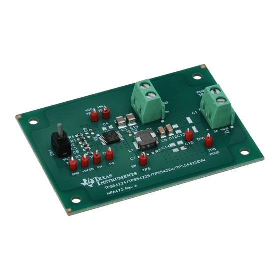
3.3 μ 2 Test Setup and Results This section describes how to properly connect, set up, and use the TPS54325 EVM. The section also includes test results typical for the evaluation modules and efficiency, output load regulation, output line regulation, load transient response, output voltage ripple, input voltage ripple, start up and switching frequency. -
Page 5: Efficiency
V = 5 V 1.025 1.000 - Output Current - A OU T Figure 2-3. TPS54325EVM Load Regulation SLVU300A – JUNE 2009 – REVISED OCTOBER 2021 TPS54325 Step-Down Converter Evaluation Module User's Guide Submit Document Feedback Copyright © 2021 Texas Instruments Incorporated... -
Page 6: Line Regulation
3 A of maximum rated load. Total peak to peak voltage variation is as shown. V (50 mV/div) I (2 A/div) 100 s/div µ Figure 2-5. TPS54325EVM Load Transient Response TPS54325 Step-Down Converter Evaluation Module User's Guide SLVU300A – JUNE 2009 – REVISED OCTOBER 2021 Submit Document Feedback Copyright © 2021 Texas Instruments Incorporated... -
Page 7: Output Voltage Ripple
2-7. The output current is the rated full load of 3 A. V (50 mV/div) SW (5 V/div) 400 ns/div Figure 2-7. TPS54325EVM Input Voltage Ripple SLVU300A – JUNE 2009 – REVISED OCTOBER 2021 TPS54325 Step-Down Converter Evaluation Module User's Guide Submit Document Feedback Copyright © 2021 Texas Instruments Incorporated... -
Page 8: Start Up
V = 1.8 V V = 3.3 V V - Input Voltage - V Figure 2-9. TPS54325EVM Switching Frequency TPS54325 Step-Down Converter Evaluation Module User's Guide SLVU300A – JUNE 2009 – REVISED OCTOBER 2021 Submit Document Feedback Copyright © 2021 Texas Instruments Incorporated... -
Page 9: Board Layout
SW1 and SW2 nodes. Also on the top layer are connections for the pins of the TPS54325 and a large area filled with power ground (PGND) connected to pins 8 and 9 of the TPS54325. The first internal layer is a split ground plane containing a large power ground (PGND) area and a smaller signal ground (GND) area. -
Page 10: Figure 3-2. Top Layer
Board Layout www.ti.com Figure 3-2. Top Layer Figure 3-3. Internal Layer 1 TPS54325 Step-Down Converter Evaluation Module User's Guide SLVU300A – JUNE 2009 – REVISED OCTOBER 2021 Submit Document Feedback Copyright © 2021 Texas Instruments Incorporated... -
Page 11: Figure 3-4. Internal Layer 2
Board Layout Figure 3-4. Internal Layer 2 Figure 3-5. Bottom Layer SLVU300A – JUNE 2009 – REVISED OCTOBER 2021 TPS54325 Step-Down Converter Evaluation Module User's Guide Submit Document Feedback Copyright © 2021 Texas Instruments Incorporated... -
Page 12: Figure 3-6. Bottom Assembly (As Viewed From Back Side)
Board Layout www.ti.com Figure 3-6. Bottom Assembly (as Viewed from Back Side) TPS54325 Step-Down Converter Evaluation Module User's Guide SLVU300A – JUNE 2009 – REVISED OCTOBER 2021 Submit Document Feedback Copyright © 2021 Texas Instruments Incorporated... -
Page 13: Schematic And Bill Of Materials
This section presents the TPS54325EVM schematic and bill of materials. 4.1 Schematic Figure 4-1 is the schematic for the TPS54325EVM. Figure 4-1. TPS54325EVM Schematic Diagram SLVU300A – JUNE 2009 – REVISED OCTOBER 2021 TPS54325 Step-Down Converter Evaluation Module User's Guide Submit Document Feedback Copyright © 2021 Texas Instruments Incorporated... -
Page 14: Bill Of Materials
IC, 3-A Single Synchronous Converter with Integrated Hi Side and PWP14 TPS54325PWP Low Side MOS FET TPS54325 Step-Down Converter Evaluation Module User's Guide SLVU300A – JUNE 2009 – REVISED OCTOBER 2021 Submit Document Feedback Copyright © 2021 Texas Instruments Incorporated... -
Page 15: References
References 5 References Texas Instruments, TPS54325 4.5-V to 18-V, 3-A Output Synchronous Step-Down SWIFT™ Controller Data Sheet 6 Revision History NOTE: Page numbers for previous revisions may differ from page numbers in the current version. Changes from Revision * (June 2009) to Revision A (October 2021) Page •... - Page 16 STANDARD TERMS FOR EVALUATION MODULES Delivery: TI delivers TI evaluation boards, kits, or modules, including any accompanying demonstration software, components, and/or documentation which may be provided together or separately (collectively, an “EVM” or “EVMs”) to the User (“User”) in accordance with the terms set forth herein.
- Page 17 www.ti.com Regulatory Notices: 3.1 United States 3.1.1 Notice applicable to EVMs not FCC-Approved: FCC NOTICE: This kit is designed to allow product developers to evaluate electronic components, circuitry, or software associated with the kit to determine whether to incorporate such items in a finished product and software developers to write software applications for use with the end product.
- Page 18 www.ti.com Concernant les EVMs avec antennes détachables Conformément à la réglementation d'Industrie Canada, le présent émetteur radio peut fonctionner avec une antenne d'un type et d'un gain maximal (ou inférieur) approuvé pour l'émetteur par Industrie Canada. Dans le but de réduire les risques de brouillage radioélectrique à...
- Page 19 www.ti.com EVM Use Restrictions and Warnings: 4.1 EVMS ARE NOT FOR USE IN FUNCTIONAL SAFETY AND/OR SAFETY CRITICAL EVALUATIONS, INCLUDING BUT NOT LIMITED TO EVALUATIONS OF LIFE SUPPORT APPLICATIONS. 4.2 User must read and apply the user guide and other available documentation provided by TI regarding the EVM prior to handling or using the EVM, including without limitation any warning or restriction notices.
- Page 20 Notwithstanding the foregoing, any judgment may be enforced in any United States or foreign court, and TI may seek injunctive relief in any United States or foreign court. Mailing Address: Texas Instruments, Post Office Box 655303, Dallas, Texas 75265 Copyright © 2019, Texas Instruments Incorporated...
- Page 21 TI products. TI’s provision of these resources does not expand or otherwise alter TI’s applicable warranties or warranty disclaimers for TI products. TI objects to and rejects any additional or different terms you may have proposed. IMPORTANT NOTICE Mailing Address: Texas Instruments, Post Office Box 655303, Dallas, Texas 75265 Copyright © 2021, Texas Instruments Incorporated...
Need help?
Do you have a question about the TPS54325 and is the answer not in the manual?
Questions and answers