Table of Contents
Advertisement
Quick Links
Advertisement
Table of Contents
Troubleshooting

Related Manuals for Panasonic KX-TG5771BXS


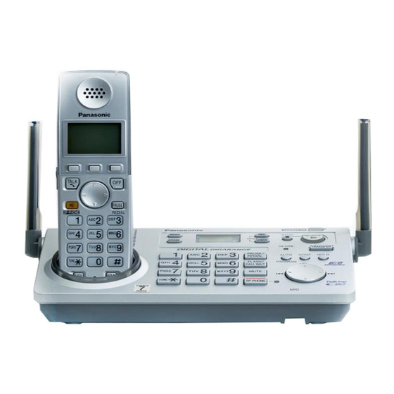
Summary of Contents for Panasonic KX-TG5771BXS
- Page 1 ORDER NO. KM40607124CE Telephone Equipment KX-TG5771BXS KX-TGA570BXS Expandable Digital Cordless Answering System Silver Version (for Asia, Middle Near East and Other areas) © 2006 Panasonic Communications Co., Ltd. All rights reserved. Unauthorized copying and distribu- tion is a violation of law.
- Page 2 KX-TG5771BXS/KX-TGA570BXS...
-
Page 3: Table Of Contents
KX-TG5771BXS/KX-TGA570BXS TABLE OF CONTENTS PAGE PAGE 1 Safety Precautions----------------------------------------------- 4 13.2. Schematic Diagram (Base Unit_Main)-------------- 86 1.1. For Service Technicians --------------------------------- 4 13.3. Schematic Diagram (Base Unit_RF Part)---------- 88 2 Warning -------------------------------------------------------------- 4 13.4. Schematic Diagram (Base Unit_Operation) ------- 90 2.1. -
Page 4: Safety Precautions
KX-TG5771BXS/KX-TGA570BXS 1 Safety Precautions 1.1. For Service Technicians ICs and LSIs are vulnerable to static electricity. When repairing, the following precautions will help prevent recurring malfunctions. 1. Cover plastic parts boxes with aluminum foil. 2. Ground the soldering irons. 3. Use a conductive mat on worktable. - Page 5 KX-TG5771BXS/KX-TGA570BXS 2.2.1. Suggested PbF Solder There are several types of PbF solder available commercially. While this product is manufactured using Tin, Silver, and Copper (Sn+Ag+Cu), you can also use Tin and Copper (Sn+Cu), or Tin, Zinc, and Bismuth (Sn+Zn+Bi). Please check the manufac- turer’s specific instructions for the melting points of their products and any precautions for using their product with other materi-...
-
Page 6: Specifications
KX-TG5771BXS/KX-TGA570BXS 3 Specifications... -
Page 7: Technical Descriptions
KX-TG5771BXS/KX-TGA570BXS 4 Technical Descriptions 4.1. FHSS Description 4.1.1. Frequency The frequency range of 5.76 GHz-5.84 GHz is used. Transmitting and receiving channel between Base Unit and Handset is same frequency. Refer to Frequency Table (P.83). 4.1.2. FHSS (Frequency Hopping Spread Spectrum) This telephone is using an IC chip which has similar specification to WDCT (World Digital Cordless Telephone) and is the tele- phone system that can use multiple portable unit simultaneously. - Page 8 KX-TG5771BXS/KX-TGA570BXS 4.1.2.1. TDD Frame Format Sync Field (72 bit): Preamble 56 bit + SyncWord 16 bit Base Unit (Handset) adjusts the timing of reception so that reception of Base Unit (Handset) can correspond to transmission of Handset (Base Unit). It is necessary for sync-field that Handset gets synchronization.
- Page 9 KX-TG5771BXS/KX-TGA570BXS 4.1.3. Signal Flowchart in the Whole System Reception CN101 of the Base Unit is connected to the TEL line, and signal is enter through the bridge diode D101. While talking, the relay (Q141) is turned ON and amplified at the Q171, then led to DSP (IC501). The DSP encodes ADPCM and TDD/TDMA with FHSS to TXMOD.
-
Page 10: Explanation Of Link Data Communication
KX-TG5771BXS/KX-TGA570BXS 4.2. Explanation of Link Data Communication 4.2.1. Calling 4.2.2. To Terminate Communication 4.2.3. Ringing... -
Page 11: Block Diagram (Base Unit_Main)
KX-TG5771BXS/KX-TGA570BXS 4.3. Block Diagram (Base Unit_Main) -
Page 12: Block Diagram (Base Unit_Rf Part)
KX-TG5771BXS/KX-TGA570BXS 4.4. Block Diagram (Base Unit_RF Part) TC_CTRL RSTN RXEN TXEN REFIN RXGAIN RXEN TXEN 5.8GHz... -
Page 13: Circuit Operation (Base Unit)
KX-TG5771BXS/KX-TGA570BXS 4.5. Circuit Operation (Base Unit) General Description: (DSP, Flash Memory) is a digital speech/signal processing system that implements all the functions of speech compression, record and playback, and memory management required in a digital telephone answering machine. The DSP system is fully controlled by a host processor DSP. The host processor provides activation and control of all that functions as follows. - Page 14 KX-TG5771BXS/KX-TGA570BXS 4.5.3. Power Supply Circuit Function: The power supply voltage from AC adaptor is converted to the desired voltage of each block. Circuit Operation: • Q300 and IC300: 4.0 V DCDC Converter • IC331: 3.3 V Regulator...
- Page 15 KX-TG5771BXS/KX-TGA570BXS 4.5.3.1. Charge Circuit The voltage from the AC adaptor is supplied to the charge circuits. Main charge (130 ~ 220 mA at the Battery) of maximum 7-hours is started soon after the Handset is placed on the Base Unit. Then it changes to Trickle charge to prevent from overcharging.
- Page 16 KX-TG5771BXS/KX-TGA570BXS 4.5.4. Reset Circuit Function: This circuit is used to initialize the microcomputer when it incorporates an AC adaptor. Circuit Operation: When the AC Adaptor is inserted into the unit, then the voltage is shifted by IC331 and power is supplied to the DSP.
- Page 17 KX-TG5771BXS/KX-TGA570BXS 4.5.5. Telephone Line Interface Telephone Line Interface Circuit: Function • Bell signal detection • ON/OFF hook and pulse dial circuit • Side tone circuit Bell signal detection and OFF HOOK circuit: In the idle mode, Q141 is open to cut the DC loop current and decrease the ring load. When ring voltage appears at the Tip (T) and Ring (R) leads (When the telephone rings), the AC ring voltage is transferred as follows: T →...
- Page 18 KX-TG5771BXS/KX-TGA570BXS 4.5.6. Auto Disconnect circuit Function: This circuit is used to detect the fact that another telephone connected to the same line is OFF-HOOK while the unit is in a receiving status or OGM transmitting status. Circuit Operation: The voltage of pin 90 of IC501 is monitored. If a parallel-connected telephone is put into OFF-HOOK status, the presence/ absence of a parallel connection is determined when the voltage changes by 0.2 V or more.
- Page 19 KX-TG5771BXS/KX-TGA570BXS 4.5.7. Parallel Connection Detect Circuit Function: In order to disable call waiting and stutter tone functions when using telephones connected in parallel, it is necessary to have a circuit that judges whether a telephone connected in parallel is in use or not. This circuit determines whether the telephone connected in parallel is on hook or off hook by detecting changes in the T/R voltage.
- Page 20 KX-TG5771BXS/KX-TGA570BXS 4.5.8. Calling Line Identification (Caller ID) Function: The caller ID is a chargeable ID which the user of a telephone circuit obtains by entering a contract with the telephone company to utilize a caller ID service. For this reason, the operation of this circuit assumes that a caller ID service contract has been entered for the circuit being used.
-
Page 21: Block Diagram (Handset_Main)
KX-TG5771BXS/KX-TGA570BXS 4.6. Block Diagram (Handset_Main) IC246 IC241 X201 FLASH EEPROM 13.824MHz Q231 MEMORY CHARGE DETECT CHG_DET OSC_IN Q361 Q362, Q363 RF part TX_DATA CHG_CTL RX_DATA CHARGE CHARGE PA_CONT CONTROL RADIO_EN D361 CON_EN R376~R379 SYN_LE2 SYN_OUT CHARGE IBAT1 SYN_DATA CURRENT IBAT2... -
Page 22: Block Diagram (Handset_Rf Part)
KX-TG5771BXS/KX-TGA570BXS 4.7. Block Diagram (Handset_RF Part) TC_CTRL RSTN RXEN TXEN REFIN RXGAIN RXEN TXEN 5.8GHz... -
Page 23: Circuit Operation (Handset)
KX-TG5771BXS/KX-TGA570BXS 4.8. Circuit Operation (Handset) 4.8.1. Construction The circuit mainly consists of DSP and RF part as shown in the block diagram. 4.8.1.1. DSP: IC201 Function • Battery Low, Power down detect circuit • Ringer Generation • Interface circuit RF part, Speaker, Mic, LED, Key scan, LCD, Headset... - Page 24 KX-TG5771BXS/KX-TGA570BXS 4.8.2. Power Supply Circuit Voltage is supplied separately to each block.
- Page 25 KX-TG5771BXS/KX-TGA570BXS 4.8.3. Charge Circuit When the Handset is put on the cradle of the Base Unit or the charger, the power is supplied from CHARGE+ and CHARGE- terminals to charge the battery via Q361 or R366, and D361. The voltage between CHARGE+ and CHARGE- flows R231 →...
- Page 26 KX-TG5771BXS/KX-TGA570BXS 4.8.5. Sending Signal The voice signal from the microphone is input to DSP (89, 90). CN331 is the headset jack. When the headphone is connected, the Q331 detect it. The input from the microphone of the Handset (MIN, MIP) is cut and the microphone signal from the headset is input to DSP (94).
-
Page 27: Circuit Operation (Rf Part)
KX-TG5771BXS/KX-TGA570BXS 4.9. Circuit Operation (RF Part) General Description: RF part includes Transmitter and Receiver functions. Digital signals (Mainly voice data) that come from DSP, are modulated and are transmitted. On the other hand, received signals are demodulated and go out to DSP. - Page 28 KX-TG5771BXS/KX-TGA570BXS 4.9.1. Power Supply Circuit As indicated below, the various voltages are supplied to each block. V_PA, about 4.0 V at Base Unit or 3.1 V at Handset, is supplied to the Power amplifier in 5.8 GHz PA circuit. IC841 is 3.0 V (Base Unit) or 2.8 V (Handset) Regulators, and IC761 is a 2.5 V Regulator. They output Vcc_5.8 GHz, and Vcc_2.4...
- Page 29 KX-TG5771BXS/KX-TGA570BXS 4.9.2. 2.4 GHz Mod/Demod Circuit IC701 incorporates all of the modulation and demodulation functions. TX Digital data (TX_DATA) from DSP is supplied to pin 27 of IC701, and then 2.4 GHz TX modulated signal is output from pin 1. This TX signal goes into the 5.8 GHz Converter circuit. 2.4 GHz RX signal from 5.8 GHz Converter circuit is passed through matching circuit and supplied to pin 4 of IC701, then demodulated...
- Page 30 KX-TG5771BXS/KX-TGA570BXS 4.9.3. 5.8 GHz Converter Circuit This block converts frequency of TX signal and RX signal. IC801 includes TX-MIXER, RX-MIXER, PLL and VCO modules internally. The VCO module is tuned by PLL synthesizer module, and generates 3.4 GHz Local signal. Reference clock (13.824 MHz) from DSP block is supplied to pin 7 of IC701.
- Page 31 KX-TG5771BXS/KX-TGA570BXS 4.9.4. 5.8 GHz PA (Power Amplifier), 5.8 GHz LNA (Low Noise Amplifier) and Antenna Switch Circuit PA block amplifies power of 5.8 GHz TX signal. 5.8 GHz TX signal from 5.8 GHz Converter circuit is filtered by 5.8 GHz-BPF FL811, and amplified by Power amplifier (PA) block of IC851.
-
Page 32: Circuit Operation (Charger Unit)
KX-TG5771BXS/KX-TGA570BXS 4.10. Circuit Operation (Charger Unit) The voltage from the AC adaptor is supplied to the charge circuits. Main charge (130 ~ 220 mA at the Battery) of maximum 7- hours is started soon after the Handset is placed on the Charger Unit. Then it changes to Trickle charge to prevent from overcharging. -
Page 33: Signal Route
KX-TG5771BXS/KX-TGA570BXS 4.11. Signal Route Each signal route is as follows. - Page 34 KX-TG5771BXS/KX-TGA570BXS Each signal route is as follows. RF part signal route...
-
Page 35: Location Of Controls And Components
KX-TG5771BXS/KX-TGA570BXS 5 Location of Controls and Components 5.1. Controls 5.1.1. Base Unit... -
Page 36: Displays
KX-TG5771BXS/KX-TGA570BXS 5.1.2. Handset 5.2. Displays 5.2.1. Base Unit Display Items 5.2.2. Handset Display Items... - Page 37 KX-TG5771BXS/KX-TGA570BXS 5.2.3. Handset Menu Icons...
-
Page 38: Installation Instructions
KX-TG5771BXS/KX-TGA570BXS 6 Installation Instructions 6.1. Setting up the Base Unit 6.2. Setting Up the Handset 6.1.1. Connecting the AC Adaptor and 6.2.1. Connecting the Charger Telephone Line Cord 6.3. Battery Installation/ Replacement 6.1.1.1. If you subscribe to a DSL service... -
Page 39: Battery Charge
Battery Charge 6.4.1. Battery Level 6.4.2. Panasonic Battery Performance Note for service: The battery strength may not be indicated correctly if the battery is disconnected and connected again, even after it is fully charged. In that case, by recharging the battery as mentioned above, you will get a correct indication of the battery strength. -
Page 40: Expanding Your Phone System
KX-TG5771BXS/KX-TGA570BXS 6.5. Expanding Your Phone System... -
Page 41: Operation Instructions
KX-TG5771BXS/KX-TGA570BXS 7 Operation Instructions 7.1. Symbols Used in These Operating Instructions... -
Page 42: Programmable Settings
KX-TG5771BXS/KX-TGA570BXS 7.2. Programmable Settings 7.2.1. Programming by Scrolling through the Display Menus... - Page 43 KX-TG5771BXS/KX-TGA570BXS...
- Page 44 KX-TG5771BXS/KX-TGA570BXS 7.2.2. Programming Using the Direct Commands...
-
Page 45: Dial Lock
KX-TG5771BXS/KX-TGA570BXS 7.3. Dial Lock For Service Hint: *: If the current password is forgotten, enter “726276642” and you will be able to go to step 3. -
Page 46: Error Messages
KX-TG5771BXS/KX-TGA570BXS 7.4. Error Messages... -
Page 47: Troubleshooting
KX-TG5771BXS/KX-TGA570BXS 7.5. Troubleshooting... - Page 48 KX-TG5771BXS/KX-TGA570BXS...
- Page 49 KX-TG5771BXS/KX-TGA570BXS...
-
Page 50: Test Mode
KX-TG5771BXS/KX-TGA570BXS 8 Test Mode 8.1. Adjustment and Test Mode Flow Chart 8.1.1. Test Burst Mode for Base Unit Note: (*1) LCD displays the Channel number. (*2) Refer to Check Table for RF part (P.67) and RX-CW Test Mode for Handset (P.55) for proper Handset settings. - Page 51 KX-TG5771BXS/KX-TGA570BXS 8.1.2. RX-CW Test Mode for Base Unit Note: (*1) LCD displays the Channel number. (*2) Refer to Check Table for RF part (P.67) and Test Burst Mode for Handset (P.54) for proper Handset settings.
- Page 52 KX-TG5771BXS/KX-TGA570BXS 8.1.3. Test Link Mode for Base Unit Note: (*1) LCD displays the Channel number. (*2) LCD displays the number of selected power. (*3) Refer to Test Link Mode for Handset (P.56). If can not proceed to the next step, refer to Registering a Handset (P.65).
- Page 53 KX-TG5771BXS/KX-TGA570BXS 8.1.4. Adjustment Mode for Base Unit Cross Reference Check and Adjust X501 (Base Unit) Frequency (P.80) Note: (*1) This is an adjustment value (hex.).
- Page 54 KX-TG5771BXS/KX-TGA570BXS 8.1.5. Test Burst Mode for Handset Note: (*1) LCD displays the Channel number. (exception: default/ CH00 = 1ch.) (*2) Refer to Check Table for RF part (P.67) and RX-CW Test Mode for Base Unit (P.51) for proper Base Unit settings.
- Page 55 KX-TG5771BXS/KX-TGA570BXS 8.1.6. RX-CW Test Mode for Handset Note: (*1) LCD displays the Channel number. (exception: default/ CH00 = 1ch.) (*2) Refer to Check Table for RF part (P.67) and Test Burst Mode for Base Unit (P.50) for proper Base Unit settings.
- Page 56 KX-TG5771BXS/KX-TGA570BXS 8.1.7. Test Link Mode for Handset Note: (*1) LCD displays the Channel number. (exception: default/ CH00 = 1ch.) (*2) If can not proceed to the next step, refer to Registering a Handset (P.65). (*3) for factory use only. (*4) Refer to Check Table for RF part (P.67) and Test Link Mode for Base Unit (P.52) for proper Base Unit settings.
- Page 57 KX-TG5771BXS/KX-TGA570BXS 8.1.8. Adjustment Mode for Handset Cross Reference (*1) Adjust Battery Low Detector Voltage (Handset) (P.80) Note: (*2) These are the default values. (*3) These values may not be fixed depending on the battery strength.
-
Page 58: Service Mode
KX-TG5771BXS/KX-TGA570BXS 9 Service Mode 9.1. How to Clear User Setting Units are reset to the Factory settings by this operation (Erase recorded Voice messages, stored Phone numbers, Caller list and etc.). This operation should not be performed for a usual repair. -
Page 59: Troubleshooting Guide
KX-TG5771BXS/KX-TGA570BXS 10 Troubleshooting Guide 10.1. Troubleshooting Flowchart Cross Reference: Note: Check Power (P.60) (*1) When a user claims that the unit disconnects a call right Error Message Table (P.60) after the greeting message and no incoming messages can Check Playback (P.62) be recorded, this symptom can not be reappeared with TEL Check Record (P.61) -
Page 60: Error Message Table
KX-TG5771BXS/KX-TGA570BXS 10.1.1. Check Power Cross Reference: Note: Power Supply Circuit (P.14) Flash Memory is IC601. Reset Circuit (P.16) DSP is IC501. (*1) Refer to Specifications (P.6) for part number and supply voltage of AC adaptor. 10.2. Error Message Table Display... - Page 61 KX-TG5771BXS/KX-TGA570BXS 10.2.1. Check Record BASE UNIT A) Not record Greeting Message B) Not record Incoming Message C) How to change the Auto Disconnect activation (time) Some Telephone Company lines (fiber or cable) ON Hook and OFF Hook voltages are lower than conventional lines, which may cause a malfunction of Auto Disconnect detection.
- Page 62 KX-TG5771BXS/KX-TGA570BXS 10.2.2. Check Playback Cross Reference: Note: Power Supply Circuit (P.14) Flash Memory is IC601. DSP is IC501. 10.2.3. Check Sp-phone Transmission Cross Reference: Note: Signal Route (P.33) Flash Memory is IC601. Telephone Line Interface (P.17) DSP is IC501. 10.2.4. Check Sp-phone Reception...
- Page 63 KX-TG5771BXS/KX-TGA570BXS 10.2.5. Check Battery Charge Note: Flash Memory is IC601. DSP is IC501. (*1) Refer to Specifications (P.6) for part number and supply voltage of AC adaptor.
- Page 64 KX-TG5771BXS/KX-TGA570BXS 10.2.6. Check Link Note: Flash Memory is IC601. DSP is IC501. (*1) Refer to Finding out the Defective part (P.65). Cross Reference: Check the RF part (P.65)
- Page 65 KX-TG5771BXS/KX-TGA570BXS 10.2.7. Check the RF part 10.2.7.1. Finding out the Defective part After All the Checkings or Repairing 1. Re-register the checked Handset to the checked Base Unit, and Regular HS to Regular BU. Note: (*1) HS: Handset (*2) BU: Base Unit...
- Page 66 KX-TG5771BXS/KX-TGA570BXS 10.2.7.1.2. Deregistering a Handset 10.2.8. RF Check Flowchart Each item (1 ~ 6) of RF Check Flowchart corresponds to Check Table for RF part (P.67). Please refer to the each item.
- Page 67 KX-TG5771BXS/KX-TGA570BXS 10.2.8.1. Check Table for RF part Item BU (Base Unit) Check HS (HandSet) Check Link Confirmation Normal 1. Register Regular HS to BU (to be 1. Register HS (to be checked) to Regular checked). HS, BU Mode [Normal Mode] 2.
- Page 68 KX-TG5771BXS/KX-TGA570BXS 10.2.9. TEST RANGE Check Circuit block which range is defective can be found by the following check. Item BU (Base Unit) Check HS (HandSet) Check Range Confirmation TX TEST 1. Register Regular HS to BU (to be checked). 1. Register HS (to be checked) to Regular BU.
- Page 69 KX-TG5771BXS/KX-TGA570BXS 10.2.9.1. RF-DSP Interface Signal Wave Form Test Burst Mode:...
- Page 70 KX-TG5771BXS/KX-TGA570BXS Test Burst Mode:...
-
Page 71: Check Handset Transmission
KX-TG5771BXS/KX-TGA570BXS 10.3. Check Handset Transmission Cross Reference: Signal Route (P.33). 10.4. Check Handset Reception Cross Reference: Signal Route (P.33). Note: When checking the RF part, Refer to Check the RF part (P.65) 10.5. Check Caller ID Cross Reference: Telephone Line Interface (P.17). -
Page 72: How To Replace The Flat Package
KX-TG5771BXS/KX-TGA570BXS 10.6. How to Replace the Flat Package IC Even if you do not have the special tools (for example, a spot heater) to remove the Flat IC, with some solder (large amount), a soldering iron and a cutter knife, you can easily remove the ICs that have more than 100 pins. - Page 73 KX-TG5771BXS/KX-TGA570BXS 10.6.3. How to Install the IC 1. Temporarily fix the FLAT PACKAGE IC, soldering the two marked pins. *Check the accuracy of the IC setting with the corresponding soldering foil. 2. Apply flux to all pins of the FLAT PACKAGE IC.
-
Page 74: How To Replace The Llp
KX-TG5771BXS/KX-TGA570BXS 10.7. How to Replace the LLP (Leadless Leadframe Package) IC 10.7.1. Preparation • PbF (: Pb free) Solder • Soldering Iron Tip Temperature of 700°F ± 20°F (370°C ± 10°C) Note: We recommend a 30 to 40 Watt soldering iron. An expert may be able to use a 60 to 80 Watt iron where someone with less experience could overheat and damage the PCB foil. - Page 75 KX-TG5771BXS/KX-TGA570BXS 10.7.4. How to Install the IC 1. Place the solder a little on the land where the radiation GND pad on IC bottom is to be attached. 2. Place the solder a little on the land where IC pins are to be attached, then place the IC.
-
Page 76: Disassembly And Assembly Instructions
KX-TG5771BXS/KX-TGA570BXS 11 Disassembly and Assembly Instructions 11.1. Disassembly Instructions 11.1.1. Base Unit... - Page 77 KX-TG5771BXS/KX-TGA570BXS 11.1.2. Handset...
- Page 78 KX-TG5771BXS/KX-TGA570BXS 11.1.3. Charger Unit...
-
Page 79: Fix The Lcd And The Receiver Guide To The Main P.c. Board (Handset)
KX-TG5771BXS/KX-TGA570BXS 11.2. Fix the LCD and the Receiver Guide to the Main P.C. Board (Handset) -
Page 80: Measurements And Adjustments
KX-TG5771BXS/KX-TGA570BXS 12 Measurements and Adjustments 12.1. Things to Do after Replacing IC 12.1.1. X501 (Base Unit), X201 (Handset) Check Equipment: Frequency counter Check Point for measurement: BCK Checking tolerance: 13.824 MHz ± 270 Hz (Base Unit)/13.824 MHz ± 100 Hz (Handset) 12.1.1.1. -
Page 81: Base Unit Reference Drawing
KX-TG5771BXS/KX-TGA570BXS 12.2. Base Unit Reference Drawing When connecting the simulator equipment for checking, please refer to below. FL881 C891 C881 FL891 FL821 R813 FL811 C856 IC300 C857 Q141 Q142 Q161 Q156 PQUP11394Z Note: (*1) is referred to No.3 of Check Table for RF part (P.67) -
Page 82: Handset Reference Drawing
KX-TG5771BXS/KX-TGA570BXS 12.3. Handset Reference Drawing When connecting the simulator equipment for checking, please refer to below. Note: (*1) is referred to No.3 of Check Table for RF part (P.67) -
Page 83: Frequency Table
KX-TG5771BXS/KX-TGA570BXS 12.4. Frequency Table 12.4.1. Base Unit Channel TX/RX Frequency (MHz) Channel TX/RX Frequency (MHz) Channel TX/RX Frequency (MHz) 5759.702398 5788.242242 5816.782086 5760.592291 5789.132135 5817.671978 5761.486139 5790.025982 5818.565826 5762.376031 5790.915875 5819.455719 5763.269879 5791.809723 5820.349566 5764.159771 5792.699615 5821.239459 5765.053619 5793.593463 5822.133307 5765.943512... - Page 84 KX-TG5771BXS/KX-TGA570BXS 12.4.2. Handset Channel TX/RX Frequency (MHz) Channel TX/RX Frequency (MHz) Channel TX/RX Frequency (MHz) 5759.700425 5788.240269 5816.780113 5760.594273 5789.134117 5817.673960 5761.484165 5790.024009 5818.563853 5762.378013 5790.917857 5819.457701 5763.267906 5791.807749 5820.347593 5764.161753 5792.701597 5821.241441 5765.051646 5793.591490 5822.131333 5765.945494 5794.485337 5823.025181 5766.835386 5795.375230...
-
Page 85: Schematic Diagram
KX-TG5771BXS/KX-TGA570BXS 13 Schematic Diagram 13.1. For Schematic Diagram 13.1.1. Base Unit (Schematic Diagram (Base Unit_Main)) 13.1.1.1. Acoustic Testing Mode Notes: 1. DC voltage measurements are taken with voltmeter from the negative voltage line. 2. The schematic diagrams may be modified at any time with the development of new technology. -
Page 86: Schematic Diagram (Base Unit_Main)
KX-TG5771BXS/KX-TGA570BXS 13.2. Schematic Diagram (Base Unit_Main) ANT0 ANT1 CON_EN CON_EN (VPA) RADIO_EN RADIO_EN RADIO_EN PA_CONT PA_CONT PA_CONT SYN_LE2 SYN_LE2 SYN_LE2 SYN_OUT SYN_OUT SYN_OUT 4.0V SYN_DATA SYN_DATA SYN_DATA SYN_CLK SYN_CLK SYN_CLK SYN_LE1 SYN_LE1 SYN_LE1 TX_DATA TX_DATA TX_DATA RX_GAIN RX_GAIN RX_GAIN RX_EN... - Page 87 KX-TG5771BXS/KX-TGA570BXS 4.0V 4.0V CONVERTOR IC331 Q300 L300 22uH VOUT VDET *RESET REFERENCE 1XX : TEL LINE 3XX : POWER, CHARGE 4XX : RESET, MIC, SP 5XX : DSP, RF I/F IC300 6XX : FLASH, KEY, LCD 7XX : RF(2.4G) ON/*OFF 8XX : RF(5.8G)
-
Page 88: Schematic Diagram (Base Unit_Rf Part)
KX-TG5771BXS/KX-TGA570BXS 13.3. Schematic Diagram (Base Unit_RF Part) 4.0V 3.0V R863 R864 5.8GHz RF FL891 TRSW_IN VDD_PA 5.8GHz_LPF FL811 5.8GHz_BPF R813 3.0V GND_ISO1 PA_IN C891 ANT1 PA_EN VCC_PA1 SYN_CLK GND_ISO2 ANTSEL_A IC851 GND_ISO3 5.8G_PA ANTSEL_B C881 VCC_PA2 VCC_TXRX 5.8GHz RF ANT2... - Page 89 KX-TG5771BXS/KX-TGA570BXS L860 PA_CONT CON_EN IC841 IC761 4.0V 3.0V_REG 2.5V_REG C766 C846 RADIO_EN L768 VRF(3.0V) VRF(2.5V) VOUT VOUT SYN_LE2 SYN_OUT SYN_DATA SYN_LE1 SYN_CLK C714 K1000P C707 K1000P 2.5V C751 D10P C708 C1.5P C713 D10P C752 K470P C735 K0.1 R747 C716 C715 TX_DATA 2.4GHz TX...
-
Page 90: Schematic Diagram (Base Unit_Operation)
KX-TG5771BXS/KX-TGA570BXS 13.4. Schematic Diagram (Base Unit_Operation) CN901 CN901 COM1 CN901 COM2 CN901 SEG3 CN901 SEG4 CN901 SEG5 CN901 SEG6 CN901 SEG7 CN901 SEG8 CN901 SEG9 CN901 SEG10 CN901 SEG11 CN901 SEG12 CN901 2APVCC CN901 LED904 MEG_LED CN901 L5DC01 LED907 ANS_LED... - Page 91 KX-TG5771BXS/KX-TGA570BXS Memo...
-
Page 92: Schematic Diagram (Handset_Main)
KX-TG5771BXS/KX-TGA570BXS 13.5. Schematic Diagram (Handset_Main) OSC_IN RSSI RSSI TX_DATA TX_DATA PA_CONT PA_CONT RX_EN RX_EN TX_EN TX_EN RX_GAIN RX_GAIN RX_DATA RX_DATA CON_EN CON_EN SYN_LE2 SYN_LE2 RADIO_EN R340 SHCTRL SHCTRL C340 K0.1 RF_RESET RF_RESET SYN_DATA SYN_DATA SYN_LE1 IC246 SYN_LE1 SYN_CLK SYN_CLK SYN_OUT... - Page 93 KX-TG5771BXS/KX-TGA570BXS TEST SIGNAL FREQUENCY:1kHz SP phone RX (MIC Mute: ON) 1.8Vp-p/8 (Vol.MAX) L327 470nH L326 470nH 2.7V Headset TX -37dBm/600 R331 50mVp-p R227 100k HEADSET_JACK CN331 R225 L331 Q331 X201 L332 C335 13.824MHZ L334 R201 22uF Headset RX 170mVp-p/150 (Vol. MAX)
-
Page 94: Schematic Diagram (Handset_Rf Part)
KX-TG5771BXS/KX-TGA570BXS 13.6. Schematic Diagram (Handset_RF Part) 3.1V R863 R864 2.8V 5.8GHz TX FL811 TRSW_IN VDD_PA 5.8GHz RF 5.8GHz_BPF R813 GND_ISO1 PA_IN C891 ANT1 PA_EN VCC_PA1 SYN_CLK GND_ISO2 ANTSEL_A IC851 GND_ISO3 5.8G_PA ANTSEL_B VCC_PA2 VCC_TXRX C881 ANT2 LNA_EN 2G4_IN GND_ISO4 LNA_GAIN... - Page 95 KX-TG5771BXS/KX-TGA570BXS L860 PA_CONT CON_EN IC841 IC761 3.1V 2.8V_REG 2.5V_REG C766 C846 ON/OFF RADIO_EN L768 VRF(2.8V) VRF(2.5V) VOUT VOUT SYN_LE2 SYN_OUT SYN_DATA 2.5V SYN_LE1 SYN_CLK C714 K1000P C707 K1000P C751 D10P C713 D10P C708 C1.5P C752 K470P C735 K0.1 R747 C716...
-
Page 96: Schematic Diagram (Charger Unit)
KX-TG5771BXS/KX-TGA570BXS 13.7. Schematic Diagram (Charger Unit) 6.5~11V NC: No Components SCHEMATIC DIAGRAM (Charger Unit) -
Page 97: Printed Circuit Board
KX-TG5771BXS/KX-TGA570BXS 14 Printed Circuit Board 14.1. Circuit Board (Base Unit_Main) 14.1.1. Component View C891 FL881 C881 FL891 FL821 R813 FL811 C856 IC300 C857 Q141 Q142 Q161 Q156 PQUP11394Z... - Page 98 KX-TG5771BXS/KX-TGA570BXS 14.1.2. Flow Solder Side View DCM2 DCP2 5761 5766 5771 5776 URX2 UTX2 BCLK PQUP11394Z DVCC JC JS CHARGE- KIN3 KIN4 CHARGE+...
-
Page 99: Circuit Board (Base Unit_Rf Part)
KX-TG5771BXS/KX-TGA570BXS 14.2. Circuit Board (Base Unit_RF Part) C891 FL881 C881 FL891 FL821 R813 FL811 C856 C857... - Page 100 KX-TG5771BXS/KX-TGA570BXS Memo...
-
Page 101: Circuit Board (Base Unit_Operation)
KX-TG5771BXS/KX-TGA570BXS 14.3. Circuit Board (Base Unit_Operation) 14.3.1. Component View... - Page 102 KX-TG5771BXS/KX-TGA570BXS 14.3.2. Flow Solder Side View...
-
Page 103: Circuit Board (Handset_Main)
KX-TG5771BXS/KX-TGA570BXS 14.4. Circuit Board (Handset_Main) 14.4.1. Component View... - Page 104 KX-TG5771BXS/KX-TGA570BXS 14.4.2. Flow Solder Side View...
-
Page 105: Circuit Board (Handset_Rf Part)
KX-TG5771BXS/KX-TGA570BXS 14.5. Circuit Board (Handset_RF Part) -
Page 106: Circuit Board (Charger Unit)
KX-TG5771BXS/KX-TGA570BXS 14.6. Circuit Board (Charger Unit) 14.6.1. Component View PQLV30043 KX-TG57 PQUP11398Z WHITE CIRCUIT BOARD (Charger Unit (Component View)) 14.6.2. Flow Solder Side View PQUP11398Z KX-TG57 PQLV30043 CIRCUIT BOARD (Charger Unit (Flow Solder Side View)) -
Page 107: Appendix Information Of Schematic Diagram
KX-TG5771BXS/KX-TGA570BXS 15 Appendix Information of Schematic Diagram 15.1. CPU Data (Base Unit) 15.1.1. IC501 Description High High_Z 60 KEY_IN6 Key In Description High High_Z 61 KEY_IN5 Key In GNDPA 62 KEY_IN4 Key In SPOUTP 63 KEY_IN3 Key In BCLK 64 KEY_IN2... -
Page 108: Cpu Data (Handset)
KX-TG5771BXS/KX-TGA570BXS 15.2. CPU Data (Handset) 15.2.1. IC201 Description High High_Z 63 STB_D Active Description High High_Z 64 STB_C Active SPOUTP 65 STB_B Active BCLK 66 STB_A Active 67 GND RSSI 68 VCC 69 TCK XOUT 70 TMS 71 TDI 72 TDO... -
Page 109: Explanation Of Ic Terminals (Rf Part)
KX-TG5771BXS/KX-TGA570BXS 15.3. Explanation of IC Terminals (RF Part) 15.3.1. IC701... - Page 110 KX-TG5771BXS/KX-TGA570BXS 15.3.2. IC801 Backside Terminal: GND...
- Page 111 KX-TG5771BXS/KX-TGA570BXS 15.3.3. IC851 Backside Terminal: GND...
-
Page 112: Terminal Guide Of The Ics, Transistors And Diodes
KX-TG5771BXS/KX-TGA570BXS 15.4. Terminal Guide of the ICs, Transistors and Diodes 15.4.1. Base Unit 15.4.2. Handset... -
Page 113: Exploded View And Replacement Parts List
KX-TG5771BXS/KX-TGA570BXS 16 Exploded View and Replacement Parts List 16.1. Cabinet and Electrical Parts (Base Unit) -
Page 114: Cabinet And Electrical Parts (Handset)
KX-TG5771BXS/KX-TGA570BXS 16.2. Cabinet and Electrical Parts (Handset) Note: (*1) Stick the MAGNETIC SHIELD (No. 124) to the exact location described above. (*2) Attach the SPACER (No. 128) to the exact location described above. -
Page 115: Cabinet And Electrical Parts (Charger Unit)
KX-TG5771BXS/KX-TGA570BXS 16.3. Cabinet and Electrical Parts (Charger Unit) -
Page 116: Accessories And Packing Materials
KX-TG5771BXS/KX-TGA570BXS 16.4. Accessories and Packing Materials 16.4.1. KX-TG5771BXS... - Page 117 KX-TG5771BXS/KX-TGA570BXS 16.4.2. KX-TGA570BXS...
-
Page 118: Replacement Parts List
KX-TG5771BXS/KX-TGA570BXS 16.5. Replacement Parts List Note: Ref. Part No. Part Name & Description Remarks 1. RTL (Retention Time Limited) PQBC10473Y2 BUTTON, NAVIGATOR KEY ABS-HB The marking (RTL) indicates that the Retention Time is PQSX10322Z KEYBOARD SWITCH, MEMO limited for this item. - Page 119 KX-TG5771BXS/KX-TGA570BXS Ref. Part No. Part Name & Description Remarks Ref. Part No. Part Name & Description Remarks CN101 K2LB102B0053 JACK R683 ERJ2GEJ821 CN301 K2ECYB000001 JACK R701 ERJ2RKF103X CN661 K1MY32BA0026 CONNECTOR R732 ERJ2GEJ100 (LCR FILTERS) R733 ERJ2GEJ100 FL811 J0E5797B0001 LCR FILTER...
- Page 120 KX-TG5771BXS/KX-TGA570BXS Ref. Part No. Part Name & Description Remarks Ref. Part No. Part Name & Description Remarks C601 ECJ0EB1A104K C856 ECJ0EC1H020C C660 ECUV1C104KBV C857 ECJ0EB0J105K C663 ECJ0EB1H102K 0.001 C865 ECUE1A333KBQ 0.033 C664 ECJ0EB1H102K 0.001 C871 F1G1HR10A561 0.1P C665 ECJ0EB1H102K 0.001...
- Page 121 KX-TG5771BXS/KX-TGA570BXS 16.5.2.2. Main P.C. Board Parts Ref. Part No. Part Name & Description Remarks Note: (COMPONENTS PARTS) (*1) When you have replaced IC201 or IC241, adjust X201. RA201 D1H84724A013 RESISTOR ARRAY Refer to Check and Adjust X201 (Handset) Frequency RA251...
- Page 122 KX-TG5771BXS/KX-TGA570BXS Ref. Part No. Part Name & Description Remarks Ref. Part No. Part Name & Description Remarks C246 ECJ0EB1A104K C773 ECJ0EC1H101J 100P C261 ECUV1C104KBV C781 ECJ0EB1A104K C262 ECUV1A105KBV C782 ECJ0EC1H121J 120P C263 ECUV1A105KBV C801 ECJ0EC1H030C C271 ECUV1C474KBV 0.47 C802 ECJ0EC1H220J...
- Page 123 KX-TG5771BXS/KX-TGA570BXS 16.5.4. Accessories and Packing Materials Note: (*1) You can download and refer to the Operating Instructions (Instruction book) on TSN Server. 16.5.4.1. KX-TG5771BXS Ref. Part No. Part Name & Description Remarks PQLV207BXZ AC ADAPTOR PQJA10075Z CORD, TELEPHONE PQJA10165Z CORD, AUDIO CABLE...
Need help?
Do you have a question about the KX-TG5771BXS and is the answer not in the manual?
Questions and answers