Panasonic KX-NT265X Service Manual
Hide thumbs
Also See for KX-NT265X:
- Brochure & specs (16 pages) ,
- Brochure & specs (16 pages) ,
- Brochure & specs (16 pages)
Table of Contents
Advertisement
Quick Links
IMPORTANT INFORMATION ABOUT LEAD FREE, (PbF), SOLDERING
If lead free solder was used in the manufacture of this product the printed circuit boards will be marked PbF.
Standard leaded, (Pb), solder can be used as usual on boards without the PbF mark.
When this mark does appear, please read and follow the special instructions described in this manual on the use of PbF and how
it might be permissible to use Pb solder during service and repair work.
IP Proprietary Telephone
KX-NT265X
KX-NT265X-B
White Version
Black Version
(for Asia, Oceania, Middle Near East, Europe, Africa
and Latin America)
© 2006 Panasonic Communications Co., Ltd. All
rights
reserved.
distribution is a violation of law.
ORDER NO. KMS0606274CE
Unauthorized
copying
and
Advertisement
Table of Contents

Subscribe to Our Youtube Channel
Related Manuals for Panasonic KX-NT265X


Summary of Contents for Panasonic KX-NT265X
- Page 1 When this mark does appear, please read and follow the special instructions described in this manual on the use of PbF and how it might be permissible to use Pb solder during service and repair work. © 2006 Panasonic Communications Co., Ltd. All rights reserved.
-
Page 2: Table Of Contents
KX-NT265X / KX-NT265X-B CONTENTS Page Page 1 ABOUT LEAD FREE SOLDER (PbF: Pb free) 10 IC DATA 1.1. SUGGESTED PbF SOLDER 10.1. IC1 (VoIP) 1.2. HOW TO RECOGNIZE THAT Pb FREE SOLDER IS 10.2. IC2 (Ethernet) USED 10.3. IC5 (DC-DC Convertor) 2 FOR SERVICE TECHNICIANS 10.4. -
Page 3: About Lead Free Solder (Pbf: Pb Free)
KX-NT265X / KX-NT265X-B 1 ABOUT LEAD FREE SOLDER (PbF: Pb free) Note: In the information below, Pb, the symbol for lead in the periodic table of elements, will refer to standard solder or solder that contains lead. We will use PbF solder when discussing the lead free solder used in our manufacturing process which is made from Tin, (Sn), Silver, (Ag), and Copper, (Cu). -
Page 4: How To Recognize That Pb Free Solder Is Used
KX-NT265X / KX-NT265X-B 1.2. HOW TO RECOGNIZE THAT Pb FREE SOLDER IS USED “PbF” is marked to show that Pb free solder is used. (See the figure below.) 2 FOR SERVICE TECHNICIANS ICs and LSIs are vulnerable to static electricity. -
Page 5: Specifications
KX-NT265X / KX-NT265X-B 3 SPECIFICATIONS Design and specifications are subject to change without notice. -
Page 6: Location Of Controls
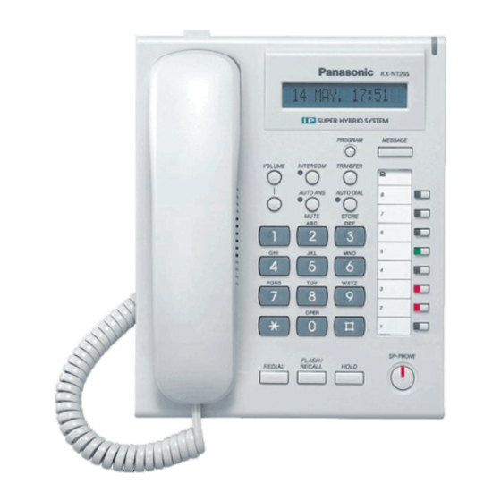
KX-NT265X / KX-NT265X-B 4 LOCATION OF CONTROLS Note: For further information, refer to the User Manual of the Hybrid IP-PBX. -
Page 7: Connection
KX-NT265X / KX-NT265X-B 5 CONNECTION CAUTION: · The AC adaptor is used as the main disconnect device. Ensure that the AC outlet is located near the unit and is easily accessible. Notes: · Consult your dealer for more details about the AC adaptor. -
Page 8: Disassembly Instructions
KX-NT265X / KX-NT265X-B 6 DISASSEMBLY INSTRUCTIONS 1. Remove the Stand. 2. Remove 5 Screws. 3. Remove the Cabinet Cover. 4. Remove the Connector from the Main Board. 5. Remove 2 Screws (A). 6. Remove the Main Board and the LCD from the Cabinet Body. - Page 9 KX-NT265X / KX-NT265X-B 7. Remove the Flat Cable from the Main Board. 8. Remove the LCD Holder by sliding the Hook in the direction of the arrow from the Main Board.
-
Page 10: Block Diagram
TXD[3:0] Trans KEY/LED/LCD TX_CLK IC12 Mll1 RX_CLK 3.3V LCD_SCK,LCD_DATA,LCD_STB RX_DV (16 x 1) LCD_CONT1,LCD_CONT2 RX_ER 5.0V To LAN RXD[3:0] 10/100Base-T 25.00 (Matrix) KEYIN[5:0],KEYOUT[5:0] GPIO Ethernet I/F IC13 12bit CO[8:3]R,CO[8:3]G GPIO BU209 (Dynamic) CO[2:1]R,CO[2:1]G GPIO 8.192 MES_R,ANS,DIAL,ICM,SP KX-NT265X/KX-NT265X-B : BLOCK DIAGRAM... -
Page 11: Circuit Operations
KX-NT265X / KX-NT265X-B 8 CIRCUIT OPERATIONS 8.1. VoIP BLOCK The DSP, MAC, CODEC and the CPU are built into the VoIP (IC1). The FLASH (IC3) and the SDRAM (IC4) are connected to the CPU. The contents of the FLASH are expanded to the SDRAM at start-up. -
Page 12: Ethernet Circuit
KX-NT265X / KX-NT265X-B 8.4. Ethernet CIRCUIT The Ethernet IC (IC2) is used for the Ethernet interface. It is connected from IC2 to the Ethernet port (JK1) through a transformer and so is isolated. Also, Ethernet port (JK1) gets power from the Ethernet line for PoE (Power-over-Ethernet) as shown below. -
Page 13: Power Supply Circuit
KX-NT265X / KX-NT265X-B 8.5. POWER SUPPLY CIRCUIT This Power Supply Circuit supports the power supply through an Ethernet line called PoE (Power-over-Ethernet) as well as the input from a regular AC adaptor. It converts the power supply from the both to 5.0V and is supplied to a 3.3V and 1.8V regulator on the MAIN board. - Page 14 KX-NT265X / KX-NT265X-B...
-
Page 15: Analog Circuit
KX-NT265X / KX-NT265X-B 8.6. ANALOG CIRCUIT This circuit performs the setting of the call path/vol. adjustment in each call mode by a built-in DSP of VoIP (IC1).The audio gain of each call is determined by download data from PBX or by internal data from flash memory (IC3). -
Page 16: Key Input Control Circuit
KX-NT265X / KX-NT265X-B 8.7. KEY INPUT CONTROL CIRCUIT The key data is under the matrix control by pin93 to 104 of IC1. The key information outputted from KEYOUT [5-0] is inputted into KEYIN [5-0], when the key is pressed. 8.8. - Page 17 KX-NT265X / KX-NT265X-B...
-
Page 18: Troubleshooting Guide
KX-NT265X / KX-NT265X-B 9 TROUBLESHOOTING GUIDE 9.1. NO OPERATION... - Page 19 KX-NT265X / KX-NT265X-B * Note: Refer to waveform(1)-(3)and(6) in 17.4. WAVEFORM (P.48).
- Page 20 KX-NT265X / KX-NT265X-B...
-
Page 21: Lcd Does Not Operate
KX-NT265X / KX-NT265X-B 9.2. LCD DOES NOT OPERATE * Note: Refer to waveform (4) in 17.4. WAVEFORM (P.48). -
Page 22: Handset Does Not Work
KX-NT265X / KX-NT265X-B 9.3. HANDSET DOES NOT WORK Receive Send... -
Page 23: Headset Does Not Work
KX-NT265X / KX-NT265X-B 9.4. HEADSET DOES NOT WORK Receive Send... -
Page 24: Speaker-Phone Does Not Work
KX-NT265X / KX-NT265X-B 9.5. SPEAKER-PHONE DOES NOT WORK Receive Send... -
Page 25: Ethernet Does Not Work (Ethernet Port)
KX-NT265X / KX-NT265X-B 9.6. Ethernet DOES NOT WORK (Ethernet PORT) * Note: Refer to waveform (7) -(12) in 17.4. WAVEFORM (P.48). -
Page 26: Led Does Not Light
KX-NT265X / KX-NT265X-B 9.7. LED DOES NOT LIGHT * Note: Refer to waveform (13) in 17.4. WAVEFORM (P.48). - Page 27 KX-NT265X / KX-NT265X-B This unit has the KEYs and LEDs TEST mode. By using this mode, you can easily check KEYs and LEDs. - To TEST mode- 1) Pushing three button (dial 3, 7 and CO1) together. Then turn on a power supply.
-
Page 28: Ic Data
KX-NT265X / KX-NT265X-B 10 IC DATA 10.1. IC1 (VoIP) Pin.No. Terminal Name I/O Setting Contents of Control Remark DGND Digital system ground Address bus Address bus Address bus Address bus Address bus Address bus Address bus Address bus Address bus... - Page 29 KX-NT265X / KX-NT265X-B Pin.No. Terminal Name I/O Setting Contents of Control Remark MWRHn External memory write signal MRDn External memory read signal RESETn Reset XTAL1 Crystal oscillator connection (8.192MHz) XTAL2 Crystal oscillator connection (8.192MHz) DVDD33 Digital system power supply (+3.3V)
- Page 30 KX-NT265X / KX-NT265X-B Pin.No. Terminal Name I/O Setting Contents of Control Remark PCMOUT/PB6 PCM data output or I/O port XDACK/PB5 Debugging control signal or I/O port DSOD/PB4 Debugging control signal or I/O port DWR/PB3 Debugging control signal or I/O port...
- Page 31 KX-NT265X / KX-NT265X-B Pin.No. Terminal Name I/O Setting Contents of Control Remark Data bus Data bus Data bus Data bus Data bus Data bus Data bus No internal connection Data bus Data bus Data bus Data bus Data bus Data bus...
-
Page 32: Ic2 (Ethernet)
KX-NT265X / KX-NT265X-B 10.2. IC2 (Ethernet) Pin.No. Terminal Name I/O Setting Contents of Control Remark MDIO MII Data I/O MII Clock Input RXD3/PHYAD MII Receive Data Output RXD2/PHYAD2 MII Receive Data Output RXD1/PHYAD3 MII Receive Data Output RXD0/PHYAD4 MII Receive Data Output VDDIO Digital IO 2.5 /3.3V tolerant power supply... -
Page 33: Ic5 (Dc-Dc Convertor)
KX-NT265X / KX-NT265X-B Pin.No. Terminal Name I/O Setting Contents of Control Remark Ground REXT External resistor VDDRCV Analog 2.5V power supply Ground Transmit Outputs Transmit Outputs VDDTX Transmitter 2.5V power supply Ground Ground XTAL feedback Crystal Oscillator Input VDDPLL Analog PLL 2.5V power supply... -
Page 34: Ic6 (Poe Interface Controller)
KX-NT265X / KX-NT265X-B 10.4. IC6 (PoE Interface Controller) Terminal Name I/O Setting Contents of Control Remark No Internal Connection. Rclass Class Select Input. No Internal Connection. Power Input. Tie to system -48V through the input diode bridge. Vout Power Output. Supplies -48V to the PD load through an internal power MOSFET that limits input current. -
Page 35: Terminal Guide Of Ics, Transistors And Diodes
KX-NT265X / KX-NT265X-B 11 TERMINAL GUIDE OF ICs, TRANSISTORS AND DIODES... -
Page 36: How To Replace A Flat Package Ic
KX-NT265X / KX-NT265X-B 12 HOW TO REPLACE A FLAT PACKAGE IC Even if you do not have the special tools (for example, a spot heater) to remove the Flat IC, with some solder (large amount), a soldering iron and a cutter knife, you can easily remove the ICs that have more than 100 pins. -
Page 37: Cabinet And Electrical Parts Location
KX-NT265X / KX-NT265X-B 13 CABINET AND ELECTRICAL PARTS LOCATION... -
Page 38: Accessories And Packing Materials
KX-NT265X / KX-NT265X-B 14 ACCESSORIES AND PACKING MATERIALS... -
Page 39: Replacement Parts List
1. RTL (Retention Time Limited) Ref. Part No. Part Name & Description Remarks Note: PSYENT265XM NAME PLATE (for KX-NT265X, Made in Malaysia) The marking (RTL) indicates that the Retention Time is PSYENT265XB NAME PLATE(for KX-NT265X-B) limited for this item. PSYENT265XBM... -
Page 40: Main Board Parts
KX-NT265X / KX-NT265X-B Ref. Part No. Part Name & Description Remarks 15.3. MAIN BOARD PARTS F1G1C104A083 Ref. Part No. Part Name & Description Remarks ECJ1VC1H180J ECJ1VC1H180J PCB1 PSWPNT265X MAIN P.C.BOARD ASS’Y (RTL) ECUV1A105ZFV When replacing the PCB1, F1G1H101A566 remove the former MAC address... - Page 41 KX-NT265X / KX-NT265X-B Ref. Part No. Part Name & Description Remarks Ref. Part No. Part Name & Description Remarks C144 F1K2E1040004 C409 F1G1C104A083 C145 F2GZZ1000006 C410 F1G1C104A083 C146 EEEFK0J101P C411 F1G1C104A083 C147 EEEFK0J101P C412 F1G1C104A083 C148 F4D25704A002 C413 F1G1C104A083 C149...
- Page 42 KX-NT265X / KX-NT265X-B Ref. Part No. Part Name & Description Remarks Ref. Part No. Part Name & Description Remarks RA26 D1H81034A024 RESISTOR ARRAY ERJ3GEYJ330 RA27 D1H81024A024 RESISTOR ARRAY ERJ3GEYJ103 RA100 D1H83904A024 RESISTOR ARRAY ERJ3GEYJ103 RA200 D1H88214A024 RESISTOR ARRAY ERJ3GEYJ330 RA201...
-
Page 43: For The Schematic Diagram
KX-NT265X / KX-NT265X-B Ref. Part No. Part Name & Description Remarks Ref. Part No. Part Name & Description Remarks R224 ERJ3GEYJ203 R248 ERJ3GEYJ151 R225 ERJ3GEYJ103 R249 ERJ3GEYJ101 R226 ERJ3GEYJ103 R250 ERJ3GEYJ101 R227 ERJ3GEYJ102 R251 ERJ3GEYJ151 R228 ERJ3GEYJ222 2.2K R252 ERJ3GEYJ151... -
Page 44: Schematic Diagram
KX-NT265X / KX-NT265X-B 17 SCHEMATIC DIAGRAM 17.1. VoIP/LCD block A[17] FLASH D3.3V A[16] A[15] D3.3V_2 BYTE A[14] VCC1 VSS46 VSS86 D[15] A[13] D[0] D[15] DQ15/A-1 DQ15 D[7] A[12] VCCQ3 VSSQ84 D[14] D[1] A[11] D[14] DQ14 DQ14 D3.3V_2 D[2] D[6] A[10]... - Page 45 KX-NT265X / KX-NT265X-B HANDSET HANDSET HEADSET HEADSET SP PHONE SP PHONE 8.1 VoIP BLOCK D3.3V Z0.1u to JTAG Z0.1u D3.3V D1.8V D3.3V RA9 33 RA12 RA13 RA14 RA15 RA16 RA17 RA18 RA19 Z0.1u D1.8V Z10u 1 DGND1 DVDD1.8_162 P1.8V 2 A15...
-
Page 46: Ethernet/Power Block
D3.3V R103 C149 #TRPBF IC10 0.7F/2.5V C147 C101 VOUT 100u/6.3V K0.01u R115 R116 C151 nDETPDN Z0.1u DC_ALARM Vout L105 DCIN+ L118 R118 100V/3A C135 DC_JACK 100k Z0.1u L106 (1/4W) DCIN- D5.0V_1 D1.8V D3.3V D3.3V_2 A3.3V C442 KX-NT265X/KX-NT265X-B Z0.1u Ethernet/POWER block... -
Page 47: Analog/Key/Led Block
17.3. ANALOG/KEY/LED block D3.3V 8.8 LED CIRCUIT C261 ANALOG CIRCUIT Z0.1u LED6 LED_C008 (13) D3.3V IC13 Handset D3.3V 1 VSS (IC1-pin115) C222 R221 R240 Reception Signal D3.3V C200 2200p C235 R234 R214 C246 2 DATA SP_DATA Z0.1u HS_OUT OE_B K10u K0.047u 3 CLOCK SP_CLK... -
Page 48: Waveform
KX-NT265X / KX-NT265X-B 17.4. WAVEFORM (1) RESET SIGNAL (2) X1 8.192MHz IC7 pin2 VDD IC1 pin34 XTAL1 IC7 pin1 nRESET (3) IC1 DR clock (4) LCD CIRCUIT CN5 pin4 RS/STB CN5 pin6 DATA/RW CN5 pin5 SCK/E IC1 pin46 DRCLK CN5 pin3 V0... - Page 49 KX-NT265X / KX-NT265X-B (7) IC2 M1 TX (8) LAN port TX 10MHz M1_TXCLK M1_TXEN Between pin1 and pin2 M1_TXD[0] Between pin40 and pin41 (9) LAN port TX 100MHz (10) IC2 M1 RX Between pin1 and pin2 M1_RXCLK M1_RXD[0] Between pin40 and pin41...
- Page 50 KX-NT265X / KX-NT265X-B (13) LED CIRCUIT IC13 pin2 DATA IC13 pin3 CLK IC13 pin4 LCK...
-
Page 51: Printed Circuit Board
C251 RA26 C240 L203 SP3P C256 C411 C220 C226 SP3M IC20 IC16 R205 C230 C214 L201 MIC3 R217 R226 C216 C202 C203 C209 IC13 C211 C225 C224 C218 IC14 C206 C200 C413 C201 C39 AG3 KX-NT265X/KX-NT265X-B MAIN BOARD COMPORNENT VIEW... -
Page 52: Main Board : Bottom View
AUTO DIAL AUTO ANS /STORE /MUTE SW19 SW18 SW17 SW11 SW24 SW23 SW22 SW16 SW21 SW29 SW28 SW27 SW26 SW30 SW33 SW32 SW31 RA27 FLASH/ REDIAL HOLD RECALL SW10 SW15 SW20 SW25 KX-NT265X/KX-NT265X-B MAIN BOARD BOTTOM VIEW T.H. KXNT265X KXNT265XB...
Need help?
Do you have a question about the KX-NT265X and is the answer not in the manual?
Questions and answers