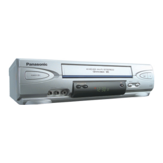
Panasonic PV-V4524S Service Manual
Video cassette recorder
Hide thumbs
Also See for PV-V4524S:
- Operating instructions manual (12 pages) ,
- Operating instructions & cook book (4 pages)
Table of Contents
Advertisement
ORDER NO. MKE0401001C1
B3
Video Cassette Recorder
PV-V4524S / PV-V4624S / PV-V464S / PV-V4524S-K / PV-454S-K /
PV-V4624S-K
For servicing the R4-Mechanism Chassis for PV-Model, Please refer to
the R4-Mechanism Chassis for PV-Model Service Manual (Order No.
MKE0401000C1).
SPECIFICATIONS
2004 Matsushita Kotobuki Electronics Industries Ltd. All rights
reserved. Unauthorized copying and distribution is a violation of law.
1
Advertisement
Table of Contents

Related Manuals for Panasonic PV-V4524S


Summary of Contents for Panasonic PV-V4524S
- Page 1 ORDER NO. MKE0401001C1 Video Cassette Recorder PV-V4524S / PV-V4624S / PV-V464S / PV-V4524S-K / PV-454S-K / PV-V4624S-K For servicing the R4-Mechanism Chassis for PV-Model, Please refer to the R4-Mechanism Chassis for PV-Model Service Manual (Order No. MKE0401000C1). SPECIFICATIONS 2004 Matsushita Kotobuki Electronics Industries Ltd. All rights...
-
Page 2: Safety Precautions
1. SAFETY PRECAUTIONS GENERAL GUIDELINES 1. IMPORTANT SAFETY NOTICE There are special components used in this equipment which are important for safety. These parts are marked by in the Schematic Diagrams, Circuit Board Layout, Exploded Views and Replacement Parts List. It is essential that these criticalparts should be replaced with manufacturerís specified parts to prevent shock, fire or other hazards. -
Page 3: Prevention Of Electro-Static Discharge
equipment such as screwheads, connectors, control shafts, etc. When the exposed metallic part has a return path to thechassis, the reading should be between 1 M and 5.2 M . When the exposed metal does not have a return path to the chassis, the reading must be infinity. LEAKAGE CURRENT HOT CHECK / (See figure 1.) 1. - Page 4 Some semiconductor (solid state) devices can be damaged easily by static electricity. Such components commonly are called Electrostatically Sensitive (ES) Devices. Examples of typical ES devices are integrated circuits, some field-effect transistorsand semiconductor "chip" components. The following techniques should be used to help reduce the incidence of component damage caused by electrostatic discharge (ESD).
-
Page 5: About Lead Free Solder (Pbf)
that provides guidelines for proper grounding and, in particular, specifies that the cable ground shall be connected to the grounding systemof the building, as close to the point of cable entry as practical.” 3. ABOUT LEAD FREE SOLDER (PbF) Distinction of PbF PCB: PCBs (manufactured) using lead free solder will have a PbF stamp or printing on the PCB. - Page 6 1. Press CH DOWN Button on VCR for over 3 seconds in Power off condition, or keep pressing CH DOWN button on VCR in Shut off condition. Fig. 1-1 2. Fault code (4-digit number) will be displayed in F.I.P. as shown. Fig.
- Page 7 Fig. 1-4 4.1.3. Explanation of Error code number The detecting condition and movement of mechanism is displayed. Fig. 1-5...
- Page 8 4.1.3.1. Reason of Ejection When an error code is 80, the reason of ejection is displayed on the Light Emitting Diode (LED) display of “TIMER”, “VCR” and “HiFi”. Fig. 1-6 Fig. 1-7...
-
Page 9: Service Notes
4.1.4. Memory and Clear of Fault Code - Error code is memorized on EEPROM (IC6004) (latest Error code only). - Error code is cleared by power on operation after a self-diagnostic display or Memory all clear. 4.2. SERVICE NOTES 4.2.1. USAGE SCREEN MODE Function displayed on the TV monitor: - the total elapsed “Cylinder rotation”... - Page 10 4.2.2. EEPROM IC (IC6004), MAIN C.B.A. REPLACEMENT NOTE After replacing EEPROM IC (IC6004) or Main C.B.A., be sure to perform the "PG SHIFTER ADJUSTMENT". NOTE: Refer to Service Manual for R4-Mechanism Chassis for PV-Model (Order No. MKE0401000C1). 4.2.3. SERVICE POSITION 4.2.3.1.
- Page 11 4.2.3.1.2. Service Position (2) Turn on the power and insert the Cassette tape. Fig. 3-2-1 After disconnecting the AC cord, turn over the Main C.B.A. and Mechanism Chassis together. Fig. 3-2-2 4.2.4. HOT CIRCUIT Primary circuit exists on the Main C.B.A. This circuit is identified as “...
- Page 12 To release from this mode, press CH UP button and CH DOWN button on VCR together again. 4.2.6. HOW TO RESET ALL VCR MEMORY FUNCTIONS To reset (clear) the select language, channel auto set and set clock functions to their initial power on condition (power on, no cassette inserted), hold down the PLAY and CH UP buttons on the unit together for more than 5 seconds.
-
Page 13: Disassembly/Assembly Procedures
Note: Refer to Item 3 of Schematic Diagram Notes of Schematic Diagram Notes, for mark “PT.” 5. DISASSEMBLY / ASSEMBLY PROCEDURES 5.1. CABINET SECTION 5.1.1. Disassembly Method NOTE: When reassembling, use the reverse steps. CAUTION:... - Page 14 Disconnect AC plug before disassembly or assembly. 5.1.1.1. Notes in chart 1. Installation of Top Cover Install the Top Cover front portion at a downward angle so that the tab on the Front Panel Assíy fits into the hole in the Top Cover. Then, lower the rear portion into place and tighten 2 Screws (447).
- Page 15 2. Installation of Front Panel Ass’y CAUTION: Opener Lever may be damaged when Front Panel Ass’y is installed, with Cassette Door-Lid of Front Panel Ass’y and Opener Lever of Cassette Up Ass’y set incorrectly. 1. When installing the Front Panel Ass’y, swing the Cassette Door-Lid all the way open until the Cassette Door tab clears the Opener Lever.
-
Page 16: Mechanism Section
B. Make sure the phase hole of the Main Cam Gear on the bottom side of Mechanism Unit is in EJECT position. Fig. D3 C. Install the Mechanism Chassis straight onto the Main C.B.A. so that the Sensor LED clears the hole in the Mechanism Chassis and that 3 Connectors (P3501, P4001, P6201) are aligned and seated securely. -
Page 17: Circuit Board Layout
6.5. SIGNAL WAVEFORMS 7. CIRCUIT BOARD LAYOUT 7.1. MAIN C. B. A. 8. BLOCK DIAGRAMS 8.1. OVERALL BLOCK DIAGRAM 9. EXPLODED VIEWS 9.1. MECHANISM SECTION... - Page 18 9.2. CHASSIS FRAME AND CASING PARTS SECTION...
-
Page 19: Packing Parts And Accessories Section
9.3. PACKING PARTS AND ACCESSORIES SECTION... -
Page 20: Replacement Parts Lists
10. REPLACEMENT PARTS LISTS BEFORE REPLACING PARTS, READ THE FOLLOWING: 10.1. REPLACEMENT NOTES 10.1.1. General Notes 1. Use only original replacement parts: To maintain original function and reliability of repaired units, use only... -
Page 21: Special Note
original replacement parts which are listed with their part numbers in the parts list. 2. IMPORTANT SAFETY NOTICE Components identified by the sign have special characteristics important for safety. When replacing any of these components, use only the specified parts. 3. -
Page 22: Mechanical Replacement Parts List
consists of a Cylinder and a Main FPC Holder (Ref. No.2). However, FPC Holder (Ref. No.2) is available separately as a replacement part. 4. The Infrared Remote Control Unit (Ref. No. 123) replacement part is available as a complete assembly unit only. Do not try to disassemble the Infrared Remote Control Unit. - Page 23 Definition of Parts supplier: 1. Parts with mark “MKE” in the Remarks column are supplied from MKE. 2. Parts without mark in the Remarks column are supplied from MKI. MECHANICAL REPLACEMENT PARTS Ref. No. Part No. Part Name & Description Remarks LSVD0009 CYLINDER KIT...
- Page 24 Ref. No. Part No. Part Name & Description Remarks VMB3550 CHANGING GEAR SPRING VMD4987 WORM BEARING 2 VMD4252 OPENER PIECE VMD4253 LED PRISM VML3624 MAIN LEVER VML3626 PINCH CHARGE ARM VML3632 IDLER ARM VDG1512 IDLER GEAR VEM0800 CAPSTAN ASS'Y VDG1637 WORM GEAR 2 VMX3377 P4 CAP 2...
-
Page 25: Electrical Replacement Parts List
Ref. No. Part No. Part Name & Description Remarks LSSC0677 GROUNDING PLATE LSSC0678 GROUNDING ANGLE VHDS0310 SCREW,STEEL XTV4+12A TAPPING SCREW,STEEL VHDS0460 SCREW,STEEL LSHD0074 SCREW,STEEL XTV26+5F TAPPING SCREW,STEEL VHD1095 SCREW,STEEL VHD1117 SCREW,STEEL XTV26+8FR TAPPING SCREW,STEEL VHD1044 SCREW,STEEL XSN3+35 SCREW,STEEL XTN26+7J SCREW,STEEL XTB3+6JFN SCREW,STEEL XTV3+12G... -
Page 26: Integrated Circuits
Definition of Parts supplier: 1. All parts are supplied from MKI. PRINTED CIRCUIT BOARD ASSEMBLY Ref. No. Part No. Part Name & Description Remarks LSEP2131HA MAIN C.B.A. ( A ) E.S.D. RTL LSEP2131HB MAIN C.B.A. ( B,C ) E.S.D. RTL LSEP2131HD MAIN C.B.A. - Page 27 Ref. No. Part No. Part Name & Description Remarks IC1001 CNC1S101R1KT IC, LINEAR IC1001 CNC1S101S1KT IC, LINEAR IC1001 PS2501-1-X IC, LINEAR IC1002 C0DAEMZ00005 IC, LINEAR IC1002 B1AZKD000001 IC, LINEAR IC1002 C0DAEMZ00001 IC, LINEAR IC3001 C1AB00002002 IC, LINEAR IC4201 AN3663FBP-V IC, LINEAR IC6001 C2CBHF000329 IC,16BIT MICROCONTROLLER E.S.D.
- Page 28 Ref. No. Part No. Part Name & Description Remarks Q3003 B1ADCF000078 TRANSISTOR SI PNP CHIP Q3005 2SD1819AHL TRANSISTOR SI NPN CHIP Q3005 B1ABCF000020 TRANSISTOR SI NPN CHIP Q3014 UNR221300L TRANSISTOR SI NPN CHIP Q3014 B1GBCFNN0004 TRANSISTOR SI NPN CHIP Q3202 2SB0709A0L TRANSISTOR SI PNP CHIP Q3202...
- Page 29 Ref. No. Part No. Part Name & Description Remarks D1001 B0EBKR000030 DIODE SI D1002 B0HAHP000014 DIODE SI D1002 B0HAJP000007 DIODE SI D1002 B0HAMP000061 DIODE SI D1002 B0HAMP000069 DIODE SI D1004 MAZ40360MF DIODE ZENER 3.6V D1005 MA2C165001VT DIODE SI D1005 B0AACK000004 DIODE SI D1005 1SS119 DIODE SI...
- Page 30 ( , , , , ) Ref. No. Part No. Part Name & Description Remarks D4207 1SS119 DIODE SI ( A,B,C,D,F ) D4208 MA2C165001VT DIODE SI ( A,B,C,D,F ) D4208 B0AACK000004 DIODE SI ( A,B,C,D,F ) D4208 1SS119 DIODE SI ( A,B,C,D,F ) D4209 MA2C165001VT DIODE SI D4209...
- Page 31 Ref. No. Part No. Part Name & Description Remarks R1210 ERJ6GEYJ122V MGF CHIP 1/10W 1.2K R1212 ERJ6GEYJ122V MGF CHIP 1/10W 1.2K R1215 ERJ6GEYJ103V MGF CHIP 1/10W 10K R1216 ERDS2TJ123T CARBON 1/4W 12K R1217 ERJ6GEYJ681V MGF CHIP 1/10W 680 R3001 ERJ3GEYJ472V MGF CHIP 1/16W 4.7K R3002 ERJ3GEYJ392V MGF CHIP 1/16W 3.9K R3003...
- Page 32 ( , , , , )
- Page 33 Ref. No. Part No. Part Name & Description Remarks R4206 ERJ3GEYJ473V MGF CHIP 1/16W 47K ( A,B,C,D,F ) R4207 ERJ3GEYJ822V MGF CHIP 1/16W 8.2K ( A,B,C,D,F ) R4208 ERJ3GEYJ822V MGF CHIP 1/16W 8.2K ( A,B,C,D,F ) R4209 ERJ3GEYJ102V MGF CHIP 1/16W 1K R4210 ERJ3GEYJ102V MGF CHIP 1/16W 1K R4213...
- Page 35 Ref. No. Part No. Part Name & Description Remarks R6046 ERJ3GEYJ102V MGF CHIP 1/16W 1K R6049 ERJ3GEYJ102V MGF CHIP 1/16W 1K R6050 ERJ3GEYJ223V MGF CHIP 1/16W 22K R6051 ERJ3GEYJ221V MGF CHIP 1/16W 220 R6053 ERJ3GEYJ221V MGF CHIP 1/16W 220 R6056 ERJ3GEYJ153V MGF CHIP 1/16W 15K R6057 ERJ3GEYJ101V MGF CHIP 1/16W 100...
- Page 36 Ref. No. Part No. Part Name & Description Remarks R6302 ERDS2TJ3R3 CARBON 1/4W 3.3 R6303 ERDS2TJ470 CARBON 1/4W 47 R6310 ERJ3GEYJ182V MGF CHIP 1/16W 1.8K R6311 ERJ3GEYJ392V MGF CHIP 1/16W 3.9K R6313 ERJ3GEYJ182V MGF CHIP 1/16W 1.8K R6314 ERJ3GEYJ392V MGF CHIP 1/16W 3.9K R6315 ERJ3GEYJ123V MGF CHIP 1/16W 12K R6316...
- Page 37 Ref. No. Part No. Part Name & Description Remarks C1204 ECEA1EKA100 ELECTROLYTIC 25V 10UF C1206 ECA1EM101I ELECTROLYTIC 25V 100UF C1209 ECEA1CKA220 ELECTROLYTIC 16V 22UF C1211 ECEA0JEE101 ELECTROLYTIC 6.3V 100UF C1212 ECEA1HKAR47 ELECTROLYTIC 50V 0.47UF C1215 ECEA1CKA100 ELECTROLYTIC 16V 10UF C1216 ECEA1HKAR47 ELECTROLYTIC 50V 0.47UF C1219...
- Page 39 Ref. No. Part No. Part Name & Description Remarks C3064 ECJ1VB1A105K C CHIP 10V 1UF C3066 ECJ1VB1C104K C CHIP 16V 0.1UF C4010 ECEA1CKA100 ELECTROLYTIC 16V 10UF C4016 ECJ1VC1H150J C CHIP 50V 15PF C4018 ECEA0JKA220 ELECTROLYTIC 6.3V 22UF C4041 ECEA1HKA2R2 ELECTROLYTIC 50V 2.2UF C4042 ECEA1EKA4R7 ELECTROLYTIC 25V 4.7UF...
- Page 41 Ref. No. Part No. Part Name & Description Remarks C4917 ECJ1VB1E104K C CHIP 25V 0.1UF C4918 ECJ1VB1E104K C CHIP 25V 0.1UF C4919 ECJ1VB1E104K C CHIP 25V 0.1UF C4920 ECJ1VB1E223K C CHIP 25V 0.022UF C5001 ECJ1VB1E103K C CHIP 25V 0.01UF C5002 ECJ1VB1E103K C CHIP 25V 0.01UF C5003...
-
Page 42: Crystal Oscillator
Ref. No. Part No. Part Name & Description Remarks C6221 ECJ1VB1H102K C CHIP 50V 1000PF C6222 ECJ1VF1A105Z C CHIP 10V 1UF C6223 ECJ1VB1H102K C CHIP 50V 1000PF C6224 ECJ1VB1H103K C CHIP 50V 0.01UF C6225 ECJ1VB1H223K C CHIP 50V 0.022UF C6226 ECJ1VB1H223K C CHIP 50V 0.022UF C6227... -
Page 43: Pin Headers
PIN HEADERS Ref. No. Part No. Part Name & Description Remarks P3501 K1MN09A00029 CONNECTOR 9P P3502 LSEK0540 GROUNDING WIRE P4001 K1MZ02A00003 FE CONNECTOR 2P P4002 K1MN06A00030 CONNECTOR 6P P6201 K1KA08A00290 CONNECTOR 8P P6202 K1KA02A00375 CONNECTOR 2P P6203 K1MN07A00017 CONNECTOR 7P SWITCHES Ref. - Page 44 Ref. No. Part No. Part Name & Description Remarks LSSZ0007 INFRARED RECEIVER UNIT B3CJZ0000004 LED DISPLAY PANEL LSJA0360 AC CORD W/PLUG,AC 120V LSJA0348 AC CORD W/PLUG,AC 120V LSJA0358 AC CORD W/PLUG,AC 120V LSJA0359 AC CORD W/PLUG,AC 120V LSJA0361 AC CORD W/PLUG,AC 120V ENG56D01G1F TUNER UHF/VHF NR ( A,B,C ) J3AAADB00001 TUNER UHF/VHF NR ( D,E,F )
- Page 45 No. Indicating what it is connected to, Model No. Identification Mark in other words, its counter part. Use the interconnection schematic diagram to find the connection between associated connectors. MODEL MARK PV-V4524S PV-V4624S Example: PV-V464S The connections between C.B.A.s are shown below. PV-V4524S-K PV-454S-K...
- Page 46 REFER TO BEGINNING OF SCHEMATIC SECTION. P4001 P6201 P0201 (2 Pins) (8 Pins) COMPARISON CHART OF TUNER MODELS & MARKS UHF/VHF MODEL MARK UHF/VHF PV-V4524S PV-V4624S UHF/VHF PV-V464S PV-V4524S-K AUDIO CONTROL/ERASE LOADING MOTOR UNIT HEAD UNIT PV-454S-K PV-V4624S-K P4092 P4002 P6202...
- Page 47 FOR SCHEMATIC DIAGRAM AND CIRCUIT BOARD LAYOUT NOTES, MODEL MARK be sure to use the part number listed in the parts list. REFER TO BEGINNING OF SCHEMATIC SECTION. PV-V4524S Do not use the part number on this diagram. PV-V4624S REC VIDEO SIGNAL PB VIDEO SIGNAL...
- Page 48 REC VIDEO SIGNAL PB VIDEO SIGNAL REC AUDIO SIGNAL PB AUDIO SIGNAL CAPSTAN SERVO Do not use the part number on this diagram. PV-V4524S PV-V4624S TO MI IIC_DATA PV-V464S TO MI IIC_CLK...
- Page 49 MODELS & MARKS For placing a purchase order of the parts, MODEL MARK be sure to use the part number listed in the parts list. PV-V4524S U6301 B3CJZ0000004 Do not use the part number on this diagram. (LED DISPLAY PANEL) PV-V4624S...
- Page 50 FOR SCHEMATIC DIAGRAM AND CIRCUIT BOARD LAYOUT NOTES, MODEL MARK be sure to use the part number listed in the parts list. REFER TO BEGINNING OF SCHEMATIC SECTION. PV-V4524S Do not use the part number on this diagram. PV-V4624S REC AUDIO SIGNAL PB AUDIO SIGNAL...
- Page 51 REFER TO BEGINNING OF SCHEMATIC SECTION. MODEL MARK Do not use the part number on this diagram. PV-V4524S PV-V4624S PV-V464S PV-V4524S-K CAUTION: FOR CONTINUED PROTECTION AGAINST FIRE HAZARD,...
- Page 52 P6202 R4104 U7001 Q4082 C4221 MODEL MARK T4101 R4040 R4203 JK3001 R4101 C4225 R4213 TUNER TP6004 R4084 WHITE Q4081 R4211 PV-V4524S TP4102 VIDEO/AUDIO UHF/VHF R4016 J4101 C4001 C4016 R4201 C4022 R4039 PV-V4624S P4002 R4011 R4652 J1005 R4081 C1222 D4201 R4013...
- Page 53 TAKEUP PHOTO TR TAKEUP PHOTO TR(L) Q6007 POSITION1-4 SW6001 SUPPLY PHOTO TR SUPPLY PHOTO TR(L) KEY DATA1-4 KEY DATA KEY SWITCH MODE SW6002 SELECT SAFETY TAB SW D6001 SENSOR LED SAFETY TAB BROKEN(H) IR DATA IR RECEIVER OVERALL BLOCK DIAGRAM PV-V4524S/PV-V4624S/PV-V464S/PV-V4524S-K/PV-454S-K/PV-V4624S-K...
- Page 54 IC3001 TP1201 11.9 Q1001 TP1202 12.4 Q1215 TP1203 TP1204 COMPARISON CHART OF -22.1 TP1205 MODELS & MARKS Q1002 TP3001 MODEL MARK Q1216 TP3002 PV-V4524S TP3009 PV-V4624S TP4002 PV-V464S PV-V4524S-K Q1003 TP4101 PV-454S-K Q3001 TP4102 PV-V4624S-K TP4103 TP4201 Q1201 TP4202 29.5...
- Page 55 Q6005 TP6203 TP6204 TP6205 TP6206 IC6005 Q6006 TP6207 TP6208 TP6301 COMPARISON CHART OF TP6302 MODELS & MARKS Q6007 TP6303 MODEL MARK TP6304 PV-V4524S TP6305 PV-V4624S IC6201 TP6306 PV-V464S PV-V4524S-K 12.3 12.3 Q6008 TP6801 PV-454S-K TP6802 PV-V4624S-K TP6803 TP6804 Q6009 TP6805 TP6806 16.4...
- Page 56 REC/PB PIN 80 OF IC6001 CUE/REV PIN 6 OF IC3001 REC/PB PIN 45 OF IC3001 REC/PB CH1 TP3002 PB SP CH2 TP6205 10ms1 10ms1 0.5V 0.5ms1 0.2V 20µs1 0.2V 5ms 2 WF13 WF18 CH1 WF23 CH2 WF1 SIGNAL WAVEFORMS PV-V4524S/PV-V4624S/PV-V464S/PV-V4524S-K/PV-454S-K/PV-V4624S-K...
- Page 57 5µs1 WF26 WF31 +14.0Vp-p +2.4Vp-p PIN 15 OF T1001 POWER ON PIN 57 OF IC4201 REC/PB 0.5ms1 5µs1 WF27 WF32 +20.0Vp-p +2.4Vp-p PIN 59 OF IC4201 REC/PB PIN 6 OF T1001 POWER ON 0.5ms1 5µs1 WF28 WF33 SIGNAL WAVEFORMS PV-V4524S/PV-V4624S/PV-V464S/PV-V4524S-K/PV-454S-K/PV-V4624S-K...
-
Page 58: Main Schematic Diagrams
PV-V4524S / PV-V4624S / PV-V464S / PV-V4524S-K / PV-454S-K / PV-V4624S-K 6.2. MAIN SCHEMATIC DIAGRAMS MAIN I (SYSTEM CONTROL / SERVO) SCHEMATIC DIAGRAM NOTE: For placing a purcha be sure to use the p Do not use the part REC VIDEO SIGNAL... - Page 59 FOR SCHEMATIC DIAGRAM AND CIRCUIT BOARD LAYOUT NOTES, MODEL MARK be sure to use the part number listed in the parts list. REFER TO BEGINNING OF SCHEMATIC SECTION. PV-V4524S Do not use the part number on this diagram. PV-V4624S PV-V464S PV-V4524S-K...
- Page 60 PV-V4524S / PV-V4624S / PV-V464S / PV-V4524S-K / PV-454S-K / PV-V4624S-K MAIN II (VIDEO SIGNAL PROCESS / AUDIO) SCHEMATIC DIAGRAM REC VIDEO SIGNAL PB VIDEO SIGNAL REC AUDIO SIGNAL PB AUDIO SIGNAL CAPSTAN SERVO TO MI IIC_DATA TO MI IIC_CLK...
- Page 61 For placing a purchase order of the parts, MODEL MARK be sure to use the part number listed in the parts list. Do not use the part number on this diagram. PV-V4524S PV-V4624S PV-V464S NOTE: PV-V4524S-K FOR SCHEMATIC DIAGRAM AND CIRCUIT BOARD LAYOUT NOTES, PV-454S-K REFER TO BEGINNING OF SCHEMATIC SECTION.
- Page 62 PV-V4524S / PV-V4624S / PV-V464S / PV-V4524S-K / PV-454S-K / PV-V4624S-K MAIN III (OPERATION) SCHEMATIC DIAGRAM U6301 B3CJZ0000004 (LED DISPLAY PANEL) TP6302 TP6301 R6683 C6306 R6684 TO MI PANE_CS C6305 TO MI MASTER_DATA_1 TO MI SCK_1 R6302 L6302 TO MV...
- Page 63 For placing a purchase order of the parts, MODEL MARK be sure to use the part number listed in the parts list. Do not use the part number on this diagram. PV-V4524S PV-V4624S PV-V464S NOTE: PV-V4524S-K FOR SCHEMATIC DIAGRAM AND CIRCUIT BOARD LAYOUT NOTES, PV-454S-K REFER TO BEGINNING OF SCHEMATIC SECTION.
- Page 64 MAIN IV (Hi-Fi) SCHEMATIC DIAGRAM NOTE: For placing a pu be sure to use t Do not use the p REC AUDIO SIGNAL PB AUDIO SIGNAL D4210 R4903 C4230 FL4901 J4201 47/6.3V C4231 R4901 C4915 TO MI MTS_MODE C4913 C4916 0.01 UNSW_+5V_SYSCON TO MV...
- Page 65 PV-V4524S / PV-V4624S / PV-V464S / PV-V4524S-K / PV-454S-K / PV-V4624S-K COMPARISON CHART OF MODELS & MARKS NOTE: NOTE: For placing a purchase order of the parts, FOR SCHEMATIC DIAGRAM AND CIRCUIT BOARD LAYOUT NOTES, MODEL MARK be sure to use the part number listed in the parts list.
- Page 66 MAIN V (POWER SUPPLY) SCHEMATIC DIAGRAM NOTE: For plac be sure Do not u CAUTION: FOR CONTINUED PROTECTION AGAINST FIRE HAZARD, IMPORTANT SAFETY NOTICE: COMPONENTS IDENTIFIED BY THE SIGN HAVE REPLACE ONLY WITH THE SAME TYPE 1.6A 125V/250V FUSE. SPECIAL CHARACTERISTICS IMPORTANT FOR SAFETY. ATTENTION:POUR UNE PROTECTION CONTINUE LES RISQUES WHEN REPLACING ANY OF THESE COMPONENTS, D' INCENDIE N' UTILISERQUE DES FUSIBLE DE MÉME...
- Page 67 PV-V4524S / PV-V4624S / PV-V464S / PV-V4524S-K / PV-454S-K / PV-V4624S-K NOTE: NOTE: COMPARISON CHART OF MODELS & MARKS For placing a purchase order of the parts, FOR SCHEMATIC DIAGRAM AND CIRCUIT BOARD LAYOUT NOTES, REFER TO BEGINNING OF SCHEMATIC SECTION.
- Page 68 PV-V4524S / PV-V4624S / PV-V464S / PV-V4524S-K / PV-454S-K / PV-V4624S-K 6.3. INTERCONNECTION SCHEMATIC DIAGRAM INTERCONNECTION SCHEMATIC DIAGRAM FULL ERASE HEAD MAIN C.B.A. P4001 P6201 (2 Pins) (8 Pins) TUNER UHF/VHF UHF/VHF UHF/VHF AUDIO CONTROL/ERASE HEAD UNIT P4092 P4002 P6202...
- Page 69 FOR SCHEMATIC DIAGRAM AND CIRCUIT BOARD LAYOUT NOTES, CAPSTAN MOTOR ASS'Y REFER TO BEGINNING OF SCHEMATIC SECTION. P0201 (8 Pins) COMPARISON CHART OF MODELS & MARKS MODEL MARK PV-V4524S PV-V4624S PV-V464S PV-V4524S-K LOADING MOTOR UNIT PV-454S-K PV-V4624S-K (2 Pins) CYLINDER UNIT...
- Page 70 VIDEO ALC CLEAR EP ON R*SVHS SYNC DEMO R*SDECK FO/DEVADJ R*SDECK MAIN EMPHASIS R*SDECK CARRIER OFFSET REC FBC+ALC W.C/D.C PB AGC+APL R*SDECK -4dB SQUE- V-AMP R*SDECK SYNC MAIN DE EMPHASIS -6dB -10dB -10dB -10dB BAND IC3001 DETAIL BLOCK DIAGRAM PV-V4524S/PV-V4624S/PV-V464S/PV-V4524S-K/PV-454S-K/PV-V4624S-K...
- Page 71 HIFI SWITCH PLAY(H) OUTPUT PREAMP SELECT & SWITCH SWITCH MODULATOR/ DEMODULATOR TUNER SWITCH NORMAL OUTPUT SWITCH AGC & SWITCH SPECTRAL INPUT SWITCH RCH INPUT SWITCH LCH SPECTRAL TIMING WIDE BAND WIDE BAND VREF TIMING GND(L) IC4201 DETAIL BLOCK DIAGRAM PV-V4524S/PV-V4624S/PV-V464S/PV-V4524S-K/PV-454S-K/PV-V4624S-K...
- Page 72 49 VSS OSD - GND terminal for OSD circuit. 99 AVDD AD - Reference power supply terminal for the AD/8bit DA. POWER 50 CV-IN Input terminal for composite video signal. 100 NC O Low fix. I/O CHART OF IC6001 PV-V4524S/PV-V4624S/PV-V464S/PV-V4524S-K/PV-454S-K/PV-V4624S-K...
Need help?
Do you have a question about the PV-V4524S and is the answer not in the manual?
Questions and answers