Samsung HT-H5500W Service Manual
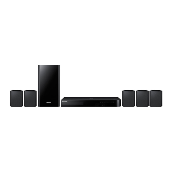
5.1ch blu-ray™ home entertainment system
Hide thumbs
Also See for HT-H5500W:
- User manual (48 pages) ,
- User manual (52 pages) ,
- User manual (100 pages)
Table of Contents
Advertisement
Quick Links
SERVICE
5.1CH Blu-ray™ Home
Entertainment System
HT-H5500W
Refer to the service manual in the GSPN (see the rear cover) for more information.
5.1CH Blu-ray™ Home
Entertainment System
Model Name
Model Code
MANUAL
1. Precaution
2. Product Specification
3. Disassembly and Reassembly
4. Troubleshooting
5. PCB Diagram
6. Schematic Diagram
HT-H5500W
HT-H5500W/ZA
Contents
Advertisement
Table of Contents

Subscribe to Our Youtube Channel
Related Manuals for Samsung HT-H5500W


Summary of Contents for Samsung HT-H5500W
- Page 1 5.1CH Blu-ray™ Home Entertainment System Model Name HT-H5500W Model Code HT-H5500W/ZA SERVICE MANUAL 5.1CH Blu-ray™ Home Contents Entertainment System 1. Precaution 2. Product Specification 3. Disassembly and Reassembly 4. Troubleshooting 5. PCB Diagram HT-H5500W 6. Schematic Diagram Refer to the service manual in the GSPN (see the rear cover) for more information.
-
Page 2: Table Of Contents
MAIN PCB Top ........................5 − 2 5.2.1. Pin Connection ......................5 − 3 5.2.2. Test Point Wave Form ....................5 − 4 5.3. MAIN PCB Bottom........................5 − 5 5.4. SMPS PCB Top (※ HT-H4500 Only)................... 5 − 6 Copyright© 1995-2013 SAMSUNG. All rights reserved. - Page 3 Pin Connection ......................5 − 7 5.5. SMPS PCB Bottom (※ HT-H4500 Only)..................5 − 8 5.6. SMPS PCB Top (※ HT-H5500W Only) ..................5 − 9 5.6.1. Pin Connection ......................5 − 10 5.7. SMPS PCB Bottom (※ HT-H5500W Only)................... 5 − 11 Schematic Diagram ...........................
-
Page 4: Precaution
TES T ALL EXPO SED METAL SU RFACES 2-WIRE C ORD ALSO TES T WITH PLUG REVER SE D (US ING AC EARTH ADAPTER PLUG GROUND AS R EQ UIRED) Figure 1.1 AC Leakage Test Copyright© 1995-2013 SAMSUNG. All rights reserved. - Page 5 A replacement part that does not have the same safety characteristics as the original might create shock, fire or other hazards. Copyright© 1995-2013 SAMSUNG. All rights reserved.
-
Page 6: Servicing Precautions
CAUTION First read the “Safety Precautions” section of this manual. If some unforeseen circumstance creates a conflict between the servicing and safety precautions, always follow the safety precautions. Copyright© 1995-2013 SAMSUNG. All rights reserved. -
Page 7: Precautions For Electrostatically Sensitive Devices (Esds)
8) Minimize body motions when handling unpackaged replacement ESDs. Motions such as brushing clothes together, or lifting a foot from a carpeted floor can generate enough static electricity to damage an ESD. Copyright© 1995-2013 SAMSUNG. All rights reserved. -
Page 8: Installation Precautions
5) Installing the product in a special place like below rather than normal environment may cause serious quality concerns due to its special conditions. If this is the case, make sure to contact a local Samsung service center before installing the product. -
Page 9: Product Specification
MP3, MKV, MP4, WMA, WMV • Support max 17 CP (Netflix, Hulu Plus, Vudu. Youtube, Opera TV etc.) • 1 USB port (Front) • Support 3D Disc • HDMI 1.4 with ARC • DLNA • Touch function key Copyright© 1995-2013 SAMSUNG. All rights reserved. -
Page 10: Specifications
170 W (3) Analog input 20 Hz ~ 20 kHz (±3 dB) Frequency response Digital input 20 Hz ~ 40 kHz (±4 dB) S/N Ratio 70 dB Channel separation 60 dB (AUX) 500 mV Input sensitivity Copyright© 1995-2013 SAMSUNG. All rights reserved. - Page 11 340 W 6.65 x 13.74 x Dimensions 3.75 x 5.7 x 2.9 3.75 x 4.5 x 2.9 8.96 x 3.75 x 2.95 (W x H x D) (inches) 11.28 1.59 1.34 1.94 8.09 Weights (Ibs) Copyright© 1995-2013 SAMSUNG. All rights reserved.
-
Page 12: Specifications Analysis
TACT Key Fuction Digital (Optical) IN 2.1 CH ~ 5.1 CH 2.1 CH ~ 5.1 CH 2.1 CH ~ 5.1 CH Speaker out Analog Audio IN O : Feature Included X : Not Included Copyright© 1995-2013 SAMSUNG. All rights reserved. -
Page 13: Accessories
2. Product Specification 2.4. Accessories 2.4.1. Supplied Accessories Accessories Item Item code Remote Control AH59-02533A Batteries (AAA size) 4301-000116 Power Cable 3903-000598 FM Antenna AH42-00021A Toroidal Ferrite Core 3301-000144 (For Power cord) User’s Manual AH68-02673A Copyright© 1995-2013 SAMSUNG. All rights reserved. -
Page 14: Disassembly And Reassembly
In order to assemble reverse the order of disassembly. Description Description Photo Unfasten 3 screws on the back. : BH,+,B,M3,L10,ZPC(BLK),SWRCH18A CAUTION Be careful not to make any scratches as you remove them. Lift the top cover. Disconnect FCC cable from Touch Key. Copyright© 1995-2013 SAMSUNG. All rights reserved. - Page 15 Unfasten 2 screws on the MAIN PCB. : BH,+,B,M3,L6,ZPC(WHT),SWRCH18A Unfasten 3 screws on the back side. : BH,+,B,M3,L10,ZPC(BLK),SWRCH18A Disassemble and lift main board. Unfasten the Assy-BT by pulling the Assy-BT up. (refer to image) Remove the Assy-BT. Copyright© 1995-2013 SAMSUNG. All rights reserved.
- Page 16 3. Disassembly and Reassembly Description Description Photo Unfasten 2 screws on the DECK. : BH,+,B,M3,L6,ZPC(WHT),SWRCH18A And push the locking points on the side. (refer to image) Remove the Assy-DECK. Copyright© 1995-2013 SAMSUNG. All rights reserved.
- Page 17 Unfasten 5 screws on the SMPS. : BH,+,B,M3,L6,ZPC(WHT),SWRCH18A 10. Unfasten 3 screws on the back side. : BH,+,B,M3,L10,ZPC(BLK),SWRCH18A Remove the SMPS and FAN. 11. Unfasten 1 screw on the Wireless RX module. : BH,+,B,M3,L6,ZPC(WHT),SWRCH18A Romove the Wireless RX module. Copyright© 1995-2013 SAMSUNG. All rights reserved.
- Page 18 3. Disassembly and Reassembly Description Description Photo 12. Unfasten 1 screw on the Wi-Fi module. : BH,+,B,M3,L10,ZPC(BLK),SWRCH18A Remove the Wi-Fi module. Copyright© 1995-2013 SAMSUNG. All rights reserved.
-
Page 19: Troubleshooting
4. Troubleshooting 4. Troubleshooting 4.1. Checkpoints by Error Mode Oscilloscope Setting Values Normal Voltage 24 MHz 32.768 KHz Voltage/DIV 1 V/div 200 mV/div 500 mV/div TIME/DIV 100 ms/div 100 ns/div 100 us/div Copyright© 1995-2013 SAMSUNG. All rights reserved. -
Page 20: No Power
CN21 #11, #12 pin Cha nge S MP S . 3.4V is OK? Ye s Does CN21 Cha nge S MP S . #6, #7, #8 pin have 12V? Ye s Cha nge MAIN P CB. Copyright© 1995-2013 SAMSUNG. All rights reserved. -
Page 21: No Audio
I2S line s a nd output No s ound on a ll cha nne ls ? Change M AIN PCB. block ha ve proble ms ? (soldering etc.) Ye s Ye s Change MAIN PCB. Re-soldering problem's components. Copyright© 1995-2013 SAMSUNG. All rights reserved. -
Page 22: Disc Loading Error
Fro nt End P owe rs Cha nge MAIN P CB. (12V, 5V, 3.3V) a re OK? Ye s Cha nge MAIN P CB. Is SP IN Motor working? Ye s Cha nge De ck. Copyright© 1995-2013 SAMSUNG. All rights reserved. -
Page 23: Remote Doesn't Work
Re fe r to wa ve pa tte rn Ye s ima ge of Fig. 4-1. Cha nge FRONT P CB. Cha nge Re mote Control. Copyright© 1995-2013 SAMSUNG. All rights reserved. - Page 24 47OHM IRR04 IRR04 IRR02 IRR02 MGND2 MGND2 DGND DGND DGND DGND N F C N 1 * 6.14. VFD/US B/TOUCH/REMOCON <Re mote Eye Da ta > * 5.2. MAIN P CB Top <Fig. 4-1> Copyright© 1995-2013 SAMSUNG. All rights reserved.
-
Page 25: No Image On Screen
IC1's re s ona tor (X376)'s cha nge this , cha nge MAIN P CB. clock is ok? Re fe r to wa ve pa tte rn ima ge of Fig. 4-3. Ye s Change MAIN PCB. Copyright© 1995-2013 SAMSUNG. All rights reserved. - Page 26 56KOHM 56KOHM 1/16W 1/16W 1/16W 1/16W HR316 HR316 HR316 HR316 HQ310 HQ310 HQ310 HQ310 HDMI_CEC_MICOM HDMI_CEC_MICOM HDMI_CEC_MICOM HDMI_CEC_MICOM * 5.2. MAIN P CB Top * 5.2. MAIN P CB Top <Fig. 4-2> <Fig. 4-2> Copyright© 1995-2013 SAMSUNG. All rights reserved.
- Page 27 TC202 TC202 DGND DGND 82PF 82PF DGND DGND IC 8 HDMI_CEC HDMI_CEC ARC_DATA+ ARC_DATA+ DGND DGND HC4005 HC4005 HR409 HR409 ARC_DATA- ARC_DATA- 0OHM 0OHM HC4006 HC4006 * 5.2. MAIN P CB Top <Fig. 4-3> Copyright© 1995-2013 SAMSUNG. All rights reserved.
-
Page 28: No Logo (Hdmi)
Check IC1's crys ta l (X376) or S ys te m Micom. singa l is OK? Re fe r to wa ve pa tte rn Ye s ima ge of Fig. 4-4. Cha nge Ma in P CB. 4-10 Copyright© 1995-2013 SAMSUNG. All rights reserved. - Page 29 TC202 DGND DGND 82PF 82PF DGND DGND IC 8 HDMI_CEC HDMI_CEC ARC_DATA+ ARC_DATA+ DGND DGND HC4005 HC4005 HR409 HR409 ARC_DATA- ARC_DATA- 0OHM 0OHM HC4006 HC4006 * 5.2. MAIN P CB Top <Fig. 4-4> Copyright© 1995-2013 SAMSUNG. All rights reserved. 4-11...
-
Page 30: Disc Skips Or Freezing
Only DVD NG? ha ve proble m? Ye s Re -s olde ring S Q10. Doe s S Q8 Cha nge De ck. ha ve proble m? Ye s Re -s olde ring S Q8. 4-12 Copyright© 1995-2013 SAMSUNG. All rights reserved. -
Page 31: No Disc Reading Error
Ele ctro nics S e rvice . on the S a ms ung We bs ite ? Ye s Upda te to the ne w ve rs ion firmwa re a nd try a ga in. Copyright© 1995-2013 SAMSUNG. All rights reserved. 4-13... -
Page 32: Network Error - Wired
The connection between LAN and SET is direct. So there is no need to check H/W if there is network problem. If it is, the problem is MAIN CHIP (IC1)'s BGA soldering problem. It must be changed to a new board. 4-14 Copyright© 1995-2013 SAMSUNG. All rights reserved. -
Page 33: Network Error - Wifi
The connection between LAN and SET is direct. So there is no need to check H/W if there is network problem. If it is, the problem is MAIN CHIP (IC1)'s BGA soldering problem. It must be changed to a new board. Copyright© 1995-2013 SAMSUNG. All rights reserved. 4-15... -
Page 34: Initialization & Upgrade Methods
Support → Contact Samsung • Description for the meaning Front : System micom S/W : BACKEND Firmware Loader : Loader Firmware Region : BD region code / DVD region code Model : Model name 4-16 Copyright© 1995-2013 SAMSUNG. All rights reserved. -
Page 35: How To Update Firmware
The update is complete when the product turns off after restarting. Press the POWER button to turn on the updated • product for your use. Samsung Electronics takes no legal responsibility for product malfunction caused by an unstable Internet connection • or consumer negligence during a software upgrade. - Page 36 3) To upgrade the firmware, select Yes. The product turns off automatically, turns on, and then begins the upgrade. 4) The update progress popup will appear. When the update is complete, the product will turn off automatically again. 5) Press the POWER button to turn on the product. 4-18 Copyright© 1995-2013 SAMSUNG. All rights reserved.
-
Page 37: Cold Start Method (Initialize Setup)
※ ※ ※ Method 1) Press “■” (STOP) button on the front panel for over 5 seconds while ‘no disc’ status. 2) Then, VFD sign : “INIT” → Power will be turned off automatically. Copyright© 1995-2013 SAMSUNG. All rights reserved. 4-19... -
Page 38: Buyer-Region Code Setting Method
4) After step 3. you can see “TEST - -” on the VFD. Insert number 46. 5) After step 4. you can see “- - -” on the VFD. Insert Region code (refer to below table) corresponding model and buyer using remote control. 4-20 Copyright© 1995-2013 SAMSUNG. All rights reserved. - Page 39 (SJ), Tunis (SJ), Nigeria (ZN), Kenya (ZN), Sudan (SJ) India (XL) Philippine (XP) BRAZIL (ZD) Table 4.2 HT-H42** 2.1CH Micom Option Table Region Code Area France (EU), Italy, Spain, Portugal, Netherlands, UK, Sweden, Turky, Germany, Austria, Greece, Poland, Hungary, Rumania, Baltic Copyright© 1995-2013 SAMSUNG. All rights reserved. 4-21...
- Page 40 Ethiopia (GA), South Africa (XA) Arab-Emirate (ZN), Parkistan (SJ), Lebanon (SJ), Iraq (SJ), Syria (SJ), Egypt (SJ), Morroco (SJ), Tunis (SJ), Nigeria (ZN), Kenya (ZN), Sudan (SJ) India (XL) Philippine (XP) BRAZIL (ZD) 4-22 Copyright© 1995-2013 SAMSUNG. All rights reserved.
- Page 41 France (EU), Italy, Spain, Portugal, Netherlands, UK, Sweden, Turky, Germany, Austria, Greece, Poland, Hungary, Rumania, Baltic Table 4.6 HT–HS52** 2.1CH Micom Option Table Region Code Area France (EU), Italy, Spain, Portugal, Netherlands, UK, Sweden, Turky, Germany, Austria, Greece, Poland, Hungary, Rumania, Baltic Copyright© 1995-2013 SAMSUNG. All rights reserved. 4-23...
-
Page 42: Pcb Diagram
8 OP EN OP EN WIRELES S WDGND1 WDGND1 WBCLK WBCLK MODULE WLRCK WLRCK WCN1(WI-FI) WDATA1 WDATA1 1 RES ET RES ET WDATA2 WDATA2 W5.0V W5.0V MAIN WIFI MODULE 5 WGND WGND WDGND2 24 WDGND2 Copyright© 1995-2013 SAMSUNG. All rights reserved. -
Page 43: Main Pcb Top
5.2. MAIN PCB Top S S C N 1 H C N 1 VC N 1 IC22 IC 8 IC 1 IC 1 WC N 1 UCN2 NFCN1 TC N 1 KC N 1 KC N 2 Copyright© 1995-2013 SAMSUNG. All rights reserved. -
Page 44: Pin Connection
PGND3 TPIC_TRAYOUT OPEN PGND2 AGND PGND1 AGND +27V_5 TPIC A+ RFO- +27V_4 TPIC A- RFO+ +27V_3 TPIC B- +27V_2 TPIC B+ FD5.0V_PW +27V_1 TPIC_MICOM WDGND2 TPIC_U GAINSW1 TPIC_V FEGIO6 TPIC_W FD3.3V_PW MDI_BD DVD_VR MDI_DVD Copyright© 1995-2013 SAMSUNG. All rights reserved. -
Page 45: Test Point Wave Form
5. PCB Diagram 5.2.2. Test Point Wave Form Copyright© 1995-2013 SAMSUNG. All rights reserved. -
Page 46: Main Pcb Bottom
5. PCB Diagram 5.3. MAIN PCB Bottom IC 3 1 IC414 Copyright© 1995-2013 SAMSUNG. All rights reserved. -
Page 47: Smps Pcb Top (※ Ht-H4500 Only)
5. PCB Diagram 5.4. SMPS PCB Top (※ ※ ※ HT-H4500 Only) Copyright© 1995-2013 SAMSUNG. All rights reserved. -
Page 48: Pin Connection
5. PCB Diagram 5.4.1. Pin Connection 1) CNM801 Power Connector Pin No. Signal PVDD PVDD PVDD PVDD PVDD A3.4V A3.4V B12V B12V B12V PS_ON -VFD +VFD Copyright© 1995-2013 SAMSUNG. All rights reserved. -
Page 49: Smps Pcb Bottom (※ Ht-H4500 Only)
5. PCB Diagram 5.5. SMPS PCB Bottom (※ ※ ※ HT-H4500 Only) Copyright© 1995-2013 SAMSUNG. All rights reserved. -
Page 50: Smps Pcb Top (※ Ht-H5500W Only)
5. PCB Diagram 5.6. SMPS PCB Top (※ ※ ※ HT-H5500W Only) Copyright© 1995-2013 SAMSUNG. All rights reserved. -
Page 51: Pin Connection
5. PCB Diagram 5.6.1. Pin Connection 1) CNM851 POWER CONNECTOR Pin No. Signal PVDD PVDD PVDD PVDD PVDD A3.4V A3.4V B12V B12V B12V PS_ON -VFD +VFD Copyright© 1995-2013 SAMSUNG. All rights reserved. 5-10... -
Page 52: Smps Pcb Bottom (※ Ht-H5500W Only)
5. PCB Diagram 5.7. SMPS PCB Bottom (※ ※ ※ HT-H5500W Only) 5-11 Copyright© 1995-2013 SAMSUNG. All rights reserved. -
Page 53: Schematic Diagram
AUDIO data. WiFi US B • HT-H4500 / HT-H5500W model supports 1 USB port. It is for USB file play like MP3, JPG and etc. H5500 S e rie s P ick-up / Loa de r • About MT8560 Audio output, I2S datas go PWM IC(TAS5538) to convert PWM signals and then go to AMP IC (TAS5614). -
Page 54: Dc-Dc Power
DGND DGND DGND DGND DGND DGND DGND DGND R12V R12V B12V_PW B12V_PW UNDEFINED UNDEFINED 0.01O HM 0.01O HM CB2012UA300T CB2012UA300T BD22 BD22 FE12V_PW FE12V_PW UNDEFINED UNDEFINED 0.01O HM 0.01O HM CB2012UA300T CB2012UA300T BD94 BD94 Copyright© 1995-2013 SAMSUNG. All rights reserved. -
Page 55: Dir/Adc/Video
47UF 47UF 1/16W 1/16W 22P F 22P F R873 R873 1/16W 1/16W 12KO HM 12KO HM C126 C126 1MOHM 1MOHM DGND DGND 12. 288M HZ 12. 288M HZ DGND DGND DGND DGND DGND DGND Copyright© 1995-2013 SAMSUNG. All rights reserved. -
Page 56: Hdmi/Arc
DGND HR3 16 HR3 16 82PF 82PF DGND DGND HDMI_CEC HDMI_CEC HQ3 10 HQ3 10 ARC_DATA+ ARC_DATA+ DGND DGND HC4005 HC4005 HR409 HR409 HDMI_CEC_M ICOM HDMI_CEC_M ICOM ARC_DATA- ARC_DATA- 0OHM 0OHM MICOM HC4006 HC4006 Copyright© 1995-2013 SAMSUNG. All rights reserved. -
Page 57: Test Point Wave Form
6. Schematic Diagram 6.4.1. Test Point Wave Form Copyright© 1995-2013 SAMSUNG. All rights reserved. -
Page 58: Nand/Ethernet/Usb/Wifi
DIR_INT1 DIR_INT1 VOUTHSYNC VOUTHSYNC REXT REXT 1/16W 1/16W 100O HM 100O HM NFC_IRQ NFC_IRQ VOUTVSYNC VOUTVSYNC 24KOHM 24KOHM 1/16W 1/16W FAST_EJECT FAST_EJECT VOUTCLK VOUTCLK R444 R444 100NF 100NF DGND DGND DGND DGND DGND DGND Copyright© 1995-2013 SAMSUNG. All rights reserved. -
Page 59: Ddr3 Bank#0
DGND1 2_K DGND1 2_K DGND1 2_K DGND DGND DGND DGND D1.5V_PW D1.5V_PW D1.5V_PW D1.5V_PW D1.5V_PW D1.5V_PW DDR3 _0.75V_VREF0_PW DDR3 _0.75V_VREF0_PW DDR3 _0.75V_VREF0_PW DDR3 _0.75V_VREF0_PW DGND DGND DGND DGND DGND DGND DGND DGND DGND DGND Copyright© 1995-2013 SAMSUNG. All rights reserved. -
Page 60: Ddr3 Bank#1
AE22 AE22 DDR3_CLK23-_CLK DDR3_CLK23-_CLK RCLK0__B RCLK0__B DDR3_0.75V _VREF0_PW DDR3_0.75V _VREF0_PW RVREF0 _B RVREF0 _B C619 C619 100NF 100NF DGND DGND DGND DGND D1.5V_PW D1.5V_PW DDR3_0.75V_VREF0_PW DDR3_0.75V_VREF0_PW D1.2V_PW D1.2V_PW DGND DGND DGND DGND DGND DGND Copyright© 1995-2013 SAMSUNG. All rights reserved. -
Page 61: Misc/Uart/Strap
[1,1,0] : NAND FRO M DIGITAL VIDEO OUTPUT PIN [1,1,1] : EMMC BO OT MODE2 [1,1,1] : EMMC BO OT MODE2 [1,0,X] : O LT MODE [1,0,X] : O LT MODE NFREN NFREN [0,1,X] : ABIST MODE [0,1,X] : ABIST MODE Copyright© 1995-2013 SAMSUNG. All rights reserved. - Page 62 TPIC_F R+ TPIC_F R+ DGND DGND TPIC_T R+ TPIC_T R+ TPIC_TR- TPIC_TR- TPIC_TILT- TPIC_TILT- TPIC_TILT+ TPIC_TILT+ MGND2 MGND2 MGND4 MGND4 TPIC_FR- TPIC_FR- TPIC_FR+ TPIC_FR+ TPIC_TR+ TPIC_TR+ DGND DGND PU_SELECT PU_SELECT DGND DGND DGND DGND 6-10 Copyright© 1995-2013 SAMSUNG. All rights reserved.
- Page 63 PUT T HES E CAPACITO RS CLO SE TO IC9340( 1391) TPIC_B+ TPIC_B+ FD5.0V_DRV_PW FD5.0V_DRV_PW C938 C938 TPIC_B- TPIC_B- COM1 COM1 TPIC_A+ TPIC_A+ TPIC_COMMON TPIC_COMMON TPIC_A- TPIC_A- TPIC_U TPIC_U TPIC_V TPIC_V TPIC_W TPIC_W C937 C937 DGND DGND DGND DGND AGND AGND AGND AGND Copyright© 1995-2013 SAMSUNG. All rights reserved. 6-11...
-
Page 64: Front Micom
DGND 22KO HM 22KO HM UR50 UR50 F_RES ET F_RES ET AL3.3V_P W AL3.3V_P W NO USE MICOM_RE SET MICOM_RE SET /RESET,RE SET /RESET,RE SET UIC2 UIC2 CAT853ST BI-GT3 CAT853ST BI-GT3 DGND DGND 6-12 Copyright© 1995-2013 SAMSUNG. All rights reserved. -
Page 65: Pwm
VPS _SW1 0.01OHM 0.01OHM 5000MA 5000MA PGND PGND 5000MA 5000MA FGND FGND Q201 Q201 VP_0 VP_0 KRC106S-R TK KRC106S-R TK VPS _SW0 VPS _SW0 KRC106S-R TK KRC106S-R TK Q202 Q202 DGND DGND DGND DGND Copyright© 1995-2013 SAMSUNG. All rights reserved. 6-13... -
Page 66: Amp
PGND 100NF 100NF 100NF 100NF 100NF 100NF PGND PGND 0.01OH M 0.01OH M PGND PGND PGND PGND DGND DGND DGND DGND PGND PGND PGND PGND DGND DGND PGND PGND PGND PGND PGND PGND 6-14 Copyright© 1995-2013 SAMSUNG. All rights reserved. -
Page 67: Vfd/Usb/Touch/Remocon
220UF AOZ8802ADI AOZ8802ADI MGND2 MGND2 DGND DGND DGND DGND DGND DGND DGND DGND DGND DGND USB1 = 1.5A CURRENT LIM IT USB1 = 1.5A CURRENT LIM IT RIGHT FRONT SCREW RIGHT FRONT SCREW Copyright© 1995-2013 SAMSUNG. All rights reserved. 6-15... -
Page 68: Test Point Wave Form
6. Schematic Diagram 6.14.1. Test Point Wave Form 6-16 Copyright© 1995-2013 SAMSUNG. All rights reserved. -
Page 69: Karaoke/Nfc/Bt
1/16W BT_I2C_SDA BT_I2C_SDA 100O HM 1/16W 100O HM 1/16W 100O HM 1/16W 100O HM 1/16W 100O HM 1/16W 100O HM 1/16W MGND2 MGND2 BT_D2 BT_D2 DGND DGND DGND DGND AOZ8802ADI AOZ8802ADI DGND DGND Copyright© 1995-2013 SAMSUNG. All rights reserved. 6-17... -
Page 70: Smps (※ Ht-H4500 Only)
6. Schematic Diagram 6.16. SMPS (※ ※ ※ HT-H4500 Only) 6-18 Copyright© 1995-2013 SAMSUNG. All rights reserved. -
Page 71: Smps-1 (※ Ht-H5500W Only)
6. Schematic Diagram 6.17. SMPS–1 (※ ※ ※ HT-H5500W Only) DA851 S DB20200P I DA851 S DB20200P I HM901 HEAT SINK LA851 LA851 +P VDD AC Block TM801S EER3541H 2.9uH(1.2P I) 2.9uH(1.2P I) (3324110203ND) ZDA851 ZDA851 DA853 S DB20200P I... -
Page 72: Smps-2 (※ Ht-H5500W Only)
6. Schematic Diagram 6.18. SMPS–2 (※ ※ ※ HT-H5500W Only) 6-20 Copyright© 1995-2013 SAMSUNG. All rights reserved. - Page 73 E.Asia, W.Asia, https://gspn2.samsungcsportal.com China, Japan N.America, S.America https://gspn3.samsungcsportal.com This Service Manual is a property of Samsung Electronics Co.,Ltd. © 2013 Samsung Electronics Co.,Ltd. Any unauthorized use of Manual can be punished under All rights reserved. applicable International and/or domestic law.
Need help?
Do you have a question about the HT-H5500W and is the answer not in the manual?
Questions and answers