Advertisement
Quick Links
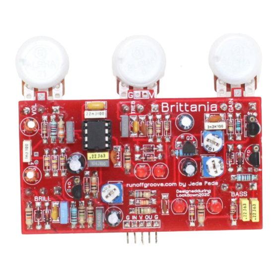
Brittania - Pedal Kit
Please read the guide in full before starting your build. It contains a lot of really important
information which will give you the best chance of a successful build.
For build support, please join our
Facebook Forum.
© Jeds Peds
truebypass@jedspeds.co.uk
Brittania
Advertisement

Related Manuals for Jeds Peds Brittania


Summary of Contents for Jeds Peds Brittania
- Page 1 Brittania - Pedal Kit Please read the guide in full before starting your build. It contains a lot of really important information which will give you the best chance of a successful build. For build support, please join our Facebook Forum.
- Page 2 Contents 1. Parts lists for this kit 2. Suggested Tools 3. A detailed overview of components 4. Populating the main PCB Jacks and the Power Socket The footswitch, its PCB and offboard wiring © Jeds Peds truebypass@jedspeds.co.uk Brittania...
- Page 3 A good search term for this would be “is xxxx an appropriate substitute for xxxx’ © Jeds Peds truebypass@jedspeds.co.uk Brittania...
- Page 4 The essential tools are all the bare minimum of what I use to build a pedal. The list is not exhaustive, but we do get a lot of enquiries about what tools people need. I sell a large range of pedal building related tools here. © Jeds Peds truebypass@jedspeds.co.uk Brittania...
- Page 5 Schematic Much thanks to the ROG team for this and the other excellent circuits they’ve designed. For a full breakdown of the Brittania – click here. This includes instructions how to get the best of your Brittania pedal once built.
- Page 6 You can either decode them yourself following the above table, alternatively this online resistor calculator or you can use a multi meter. If you want any further explanation about how to decode resistor values, this video may help. © Jeds Peds truebypass@jedspeds.co.uk Brittania...
- Page 7 Aim for a maximum of 4 seconds. Less is good! If you have more than one diode to solder it is good practice to do one leg on each then go back for the second. This way the diode has time to cool between each leg being soldered. © Jeds Peds truebypass@jedspeds.co.uk Brittania...
- Page 8 The transistor can be the one listed or any other suitable substitute with matching pin out. The orientation of this part is crucial. The silkscreen layer indicates which way around it needs to be with its transistor shaped outline, matching the transistors case. Solder this very carefully. © Jeds Peds truebypass@jedspeds.co.uk Brittania...
- Page 9 Solder these in place without the chip, totally protecting the chip from heat. Please check you have all pins through the pads before you begin soldering the socket. © Jeds Peds truebypass@jedspeds.co.uk Brittania...
- Page 10 Polarised capacitors can only be inserted into the board in one direction. The PCB will have a + next to the positive terminal. © Jeds Peds truebypass@jedspeds.co.uk Brittania...
- Page 11 On the capacitor you will see that one side of the can is marked with a stripe usually containing negative symbols. The wire nearest to this is the negative wire. You will also notice that the positive wire is longer. © Jeds Peds truebypass@jedspeds.co.uk Brittania...
- Page 12 PCB ensuring that you solder them in place well as you go. I then add the pots either mounting them to the board or wiring them into place. © Jeds Peds truebypass@jedspeds.co.uk Brittania...
- Page 13 1, or both. The pin numbers are the same for both types of pot. Just behind pin 1 and next to the shaft is a small metal tag. Take a pair of pliers and snap this off. It comes away easily. © Jeds Peds truebypass@jedspeds.co.uk Brittania...
- Page 14 The pots connect to the PCB like this, by this stage you should have soldered the resistors, diode, transistors and capacitors etc to the board. Now the final step is to connect the pots as shown. © Jeds Peds truebypass@jedspeds.co.uk...
- Page 15 The above is for centre negative power supplies. Should you have the opposite you must reverse the connections. At this stage, connect two long wires to the socket as shown and set it aside. There is no need to put anything in the enclosure just yet. © Jeds Peds truebypass@jedspeds.co.uk Brittania...
- Page 16 Take one wire from one tip and solder it to the IN pad. This is now your test phase input jack. Take the final tip wire and solder it to the OU pad. This is now your test phase output jack. © Jeds Peds truebypass@jedspeds.co.uk Brittania...
- Page 17 If your PCB is working you are ready to connect the board to the footswitch! Follow the next stages meticulously and all being well by the end of it you will have a lovely finished pedal! © Jeds Peds truebypass@jedspeds.co.uk...
- Page 18 About 2 inches long will be perfect, a little longer if you wish. They will be cut to length later. Cut the ground joint and strip the ends of all wires again so they are fresh. The PCB should have 4 wires coming from it all about 5/6 inches long. © Jeds Peds truebypass@jedspeds.co.uk Brittania...
- Page 19 Once you are satisfied it is on the right way then it must be soldered into place, but don’t do it yet as I want to explain a second method of switch wiring that you may decide suits you better. (if you have already decided that you want to use the 3PDT PCB, then follow this link) © Jeds Peds truebypass@jedspeds.co.uk Brittania...
- Page 20 The footswitch has a ground lug. The same goes for all V pads. V is the direct power feed. So you must connect power to the CLR and to the V pad on the main PCB © Jeds Peds truebypass@jedspeds.co.uk Brittania...
- Page 21 I do suggest this as it is neater and less confusing. The PCB is double sided, and here are pictures of both sides. Side 1 Side 2 Eventually side two will face out of the enclosure. © Jeds Peds truebypass@jedspeds.co.uk Brittania...
- Page 22 Here is an overview of the connections on the PCB. © Jeds Peds truebypass@jedspeds.co.uk Brittania...
- Page 23 To give you an idea about this I have shown the connections for the G and V. The IN pads also require a connection, as does the OU. You should have 4 wires running between the two PCBs. © Jeds Peds truebypass@jedspeds.co.uk Brittania...
- Page 24 Once all connections are complete you should have a pedal to test! If it does not work and you can’t spot an error, don’t forget we have the Facebook forum to guide you. Good Luck and happy soldering Love Jed x © Jeds Peds truebypass@jedspeds.co.uk Brittania...
Need help?
Do you have a question about the Brittania and is the answer not in the manual?
Questions and answers