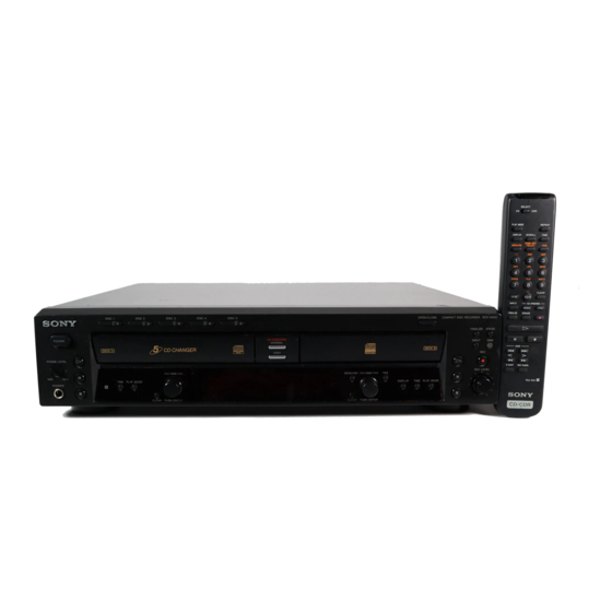
Sony RCD-W50C Service Manual
Hide thumbs
Also See for RCD-W50C:
- Operating instructions manual (35 pages) ,
- Dimensions (1 page) ,
- Manual (51 pages)
Table of Contents
Advertisement
Quick Links
SERVICE MANUAL
Ver 1.1 2003. 12
DECK A (the CD player section)
System
Compact disc digital audio
system
Laser
Semiconductor laser (λ =
780 nm)
Emission duration:
continuous
Frequency response
20 Hz – 20,000 Hz (±0.5
dB)
DECK B (the CD-R and CD-RW
recording section)
System
Compact disc digital audio
system
Laser
Semiconductor laser (λ =
780 nm)
Emission duration:
continuous
Playable discs
CD, CD-R, CD-RW
Recordable discs
CD-R, CD-RW (for music
use)
Frequency response
20 Hz - 20,000 Hz (±0.5
dB)
Sony Corporation
9-874-151-02
2003L16-1
Home Audio Company
© 2003.12
Published by Sony Engineering Corporation
RCD-W50C
Model Name Using Similar Mechanism
CD Mechanism Type
CD Section
Base Unit Type
Optical Pick-up Type
Model Name Using Similar Mechanism
CD-R/CD-RW CD Mechanism Type
Section
Base Unit Type
Optical Pick-up Type
SPECIFICATIONS
Inputs
ANALOG IN
(Phono jacks)
Impedance: 47 kilohms
Rated input: 500 mVrms
Minimum input
250 mVrms
DIGITAL OPTICAL IN
(Square optical connector jack)
Optical wavelength:
660 nm
Outputs
ANALOG OUT
(Phono jacks)
Impedance: 47 kilohms
Rated output: 2 Vrms
Load impedance: over
10 kilohms
DIGITAL OPTICAL OUT
(Square optical connector jack)
Wavelength: 660 nm
Output level: –18 dBm
PHONES
(Phono jack)
Load impedance: 32 ohms
Output level: 12mW
Canadian Model
NEW
CDM53L-30B61B
BU-30BBD61B
A-MAX.3
NEW
CDM65-RBD1
RBD1
KRM-220CAA
General
Power requirements
North American model:
120 V AC, 60 Hz
Other models:
110-120/220-240V AC,
50/60 Hz
Power consumption
25 W
Dimensions (approx.) (w/h/d) incl. projecting parts
430 × 108 × 399 mm
and control
( 17 × 4
Mass (approx.)
6.8 kg
(15 lbs)
Supplied accessories
• Audio connecting cords
• Remote commander (remote) (1)
• Size AA (R6) batteries (2)
Design and specifications are subject to change
without notice.
COMPACT DISC RECORDER
US Model
E Model
× 15
3
/
3
/
inch)
8
4
Phono jack × 2 (red/white) ↔
Phono jack × 2 (red/white) (2)
Advertisement
Table of Contents

Related Manuals for Sony RCD-W50C


Summary of Contents for Sony RCD-W50C
- Page 1 20 Hz - 20,000 Hz (±0.5 Wavelength: 660 nm Output level: –18 dBm PHONES (Phono jack) Load impedance: 32 ohms Output level: 12mW COMPACT DISC RECORDER Sony Corporation 9-874-151-02 2003L16-1 Home Audio Company © 2003.12 Published by Sony Engineering Corporation...
- Page 2 DIAGRAMMES SCHÉMATIQUES ET LA LISTE DES PIÈCES SONT 4-238-401-1π Canadian CRITIQUES POUR LA SÉCURITÉ DE FONCTIONNEMENT. NE 4-238-401-3π REMPLACER CES COMPOSANTS QUE PAR DES PIÈSES SONY DONT LES NUMÉROS SONT DONNÉS DANS CE MANUEL OU DANS LES SUPPÉMENTS PUBLIÉS PAR SONY.
-
Page 3: Table Of Contents
RCD-W50C TABLE OF CONTENTS Unleaded solder 1. SERVICING NOTE ····················································· Boards requiring use of unleaded solder are printed with the lead- 2. GENERAL ··································································· free mark (LF) indicating the solder contains no lead. (Caution: Some printed circuit boards may not come printed with 3. -
Page 4: Servicing Note
RCD-W50C SECTION 1 SERVICING NOTE Self-diagnosis Function NOTES ON HANDLING THE OPTICAL PICK-UP BLOCK OR BASE UNIT When the self-diagnosis function is activated to The laser diode in the optical pick-up block may suffer electrostatic prevent the player from malfunctioning, three... -
Page 5: General
RCD-W50C SECTION 2 GENERAL POWER button PLAY MODE button H button TIME button DISC 1 to DISC 5 A button and indicators DISPLAY button CD SYNCHRO NORMAL button YES button CD SYNCHRO HIGH button l AMS L knob OPEN/CLOSE A button... -
Page 6: Disassembly
RCD-W50C SECTION 3 DISASSEMBLY Note : Disassemble the unit in the order as shown below. CASE (409538) LOADING PANEL (CDR) FRONT PANEL SECTION CD-SW board, LED board, DISPLAY board CD MECHANISM DECK (CDM65-RBD1) TRAY CDR BOARD MOTOR ASSEMBLY (LOADING) (M201) -
Page 7: Case (409538)
RCD-W50C Note : Follow the disassembly procedure in the numerical order given. 3-1. Case (409538) 4 case (409538) 3 two screws 2 two screws (case 3 TP2 3 × 8 ) (case 3 TP2 3 × 8 ) 1 two screws (case 3 TP2 3 ×... -
Page 8: Front Panel Section
RCD-W50C 3-3. Front Panel Section 1 connector (2core)(CN900) 4 connector (2core)(CN920) 5 three screws (+BVTP 3 × 8) 2 connector (3core)(CN690) 3 flexible flat cable (21core) (CN671) 7 t wo claws 8 front panel section 6 four screws (+BVTP 3 × 8) 3-4. -
Page 9: Cd Mechanism Deck (Cdm65-Rbd1)
RCD-W50C 3-5. CD Mechanism Deck (CDM65-RBD1) 3 four screws (+BVTP 3 × 8) 2 flexible flat cable (11core) (CN630) 4 CD mechanism deck (CDM65-RBD1) 1 connector (CN631) 3-6. Tray 2 Pull the tray while pressing the claw of 1 Slide the lever (cam (CH)) to the direction of arrow. -
Page 10: Cdr Board
RCD-W50C 3-7. CDR Board 1 four screws (+BVTP 2.6 × 8) 2 bottom plate 9 CDR board 3 flexible flat cable (32core) (CN101) 5 flexible flat cable (11core) (CN103) 4 flexible flat cable (11core) (CN102) 6 c law 7 c law... -
Page 11: Optical Pick-Up (Krm-220Caa)
RCD-W50C 3-9. Optical Pick-Up (KRM-220CAA) 2 two screws 1 two step screws ((2X9) (G with), +p tappin) 3 two insulators (main) 6 optical pick-up (KRM-220CAA) 4 two insulators (main) 5 flexible flat cable (32core) (from optical device) 3-10. Motor Assembly (Loading) (M201) 1 Slide the cam (CH) to the direction of arrow. -
Page 12: Cam (Ch)
RCD-W50C 3-11. Cam (CH) q; Slide the cam (CH) to the 6 screw 5 holder (BU) sub assembly (+PTPWH 2.6 × 8) direction of arrow A while pressing the claw. 7 g ear (C) qs cam (CH) claw cam (CH) -
Page 13: Cd Mechanism Deck (Cdm53L-30B61B)
RCD-W50C 3-13. CD Mechanism Deck (CDM53L-30B61B) 2 four screws (+BVTP 3 × 8) 5 CD mechanism deck (CDM53L-30B61B) 1 connector (CN641) 4 flexible flat cable 3 flexible flat cable (17core) (CN701) (23core) (CN101) 3-14. Fitting Base (Magnet) Assembly 2 four screws (+BTTP M2.6 ) -
Page 14: Clamp Motor Board
RCD-W50C 3-15. CLAMP MOTOR Board, Motor (Clamp) Assembly (M701) 1 belt (mode) 5 motor (clamp) assembly (M701) 4 CLAMP MOTOR board 3 Remove the two solderings. 2 two screws (+BTTP M2.6) 3-16. Fitting Base (Guide) Assembly, Bracket (Chassis) 2 four screws (+BVTP 2.6 ×... -
Page 15: Tray (Sub)
RCD-W50C 3-17. Tray (Sub) 1 Rotating the pulley (LD), shift the slider (selection) in the arrow A direction. 2 Rotating the pulley (mode) in the arrow direction, adjust the tray (sub) to be removed. 3 Rotating the pulley (LD), shift the slider (selection) in the arrow B direction. -
Page 16: Load Motor Board, Motor (Loading) Assembly (M702)
RCD-W50C 3-19. LOAD MOTOR Board, Motor (Loading) Assembly (M702) 1 belt (communication) 2 belt (loading1) 3 belt (loading1) 7 motor (loading) assembly (M702) 6 LOAD MOTOR board 5 Remove the two solderings. 4 two screws (+BTTP M2.6) 3-20. Stocker Section... -
Page 17: Slider (Selection), Tension Spring (Shutter)
RCD-W50C 3-21. Slider (Selection), Tension Spring (Shutter), Slider (Shutter) 1 two floating screws PRECAUTION DURING SLIDER (+PTPWHM 2.6 x 6) (SELECTION) INSTALLATION (2) 2 washer Insert the slider (selection) 4 slider (selection), into the portion A. tension spring (shutter), slider (shutter) -
Page 18: Precaution During Gear (Gear U/D Slider), Gear (Gear B), Gear (Gear A) Installation
RCD-W50C Precaution During Gear (Gear U/D Slider), Gear (Gear B), Gear (Gear A) Installation 3 gear (gear B) portion A Adjust the gear (gear B) with the portion A as shown. slider (U/D) 1 Slide the slider (U/D) fully in the arrow direction. -
Page 19: Bd Board
RCD-W50C 3-24. BD Board Remove soldering from the four points. 4 BD board 1 flexible flat cable (16core) (CN102) 3 hook 3-25. Optical Block Section 4 optical block section 1 two floating screws (+PTPWHM 2.6) shaft (BU holder) gear (chucking) Rotate the pulley (LD) in the direction of 2 to move the shaft (BU holder) upper. - Page 20 RCD-W50C MEMO...
-
Page 21: Test Mode
RCD-W50C SECTION 4 TEST MODE Setting the Test Mode BU Test Mode (Deck A) Procedure: Procedure: 1. Press the POWER button to POWER on. 1. Enter the test mode, then turn the l AMS L (DECK B) 2. Press the l AMS L (DECK A), [SBM] and l AMS knob to display “BU Test”, and press the l AMS L... - Page 22 RCD-W50C FL ALL OFF Mode CDR History Display Procedure: Procedure: 1. Enter the test mode, then turn the l AMS L (DECK B) 1. Enter the test mode, then turn the l AMS L (DECK B) knob to display “FL ALL OFF”, and press the l AMS L knob to display “CDR History”, and press the l AMS L...
- Page 23 RCD-W50C 3 Operation mode 5 Write POWER (integer of mW x 10, available during write bit 7: Speed processing) 0: normal speed examples: 00 means unavailable 1: x4 speed (when 3 operation mode is not recording) bit 6 to bit 0: Number of inner condition : A3 means 163(decimal), i.e.
-
Page 24: Electrical Adjustments
RCD-W50C SECTION 5 ELECTRICAL ADJUSTMENTS Note: A clear RF signal waveform means that the shape “◊” can be CD SECTION (DECK A) clearly distinguished at the center of the waveform. Note : 1. CD Block is basically designed to operate without adjustment. -
Page 25: Cd-R/Rw Section
RCD-W50C CD-R/RW SECTION The following is the method of locating the faulty point and (w/ Serial I/F) electrical adjustment. Connection and Setting of Programs COM1 1-1. Connection RCD-W50C RS-232C Cable Oscilloscope MPXOUT 0-756-358-11 CDM65-RBD1 SERVICE CONTROL FIRM RESET Cables for Jig connecting... - Page 26 RCD-W50C 1-2. Equipments to prepare Test Object Both RBD1 and CDM65-RBD1 shall be tested. RBD1 : Flash Memory Writing of of Circuit Test by Self-diagnostics CDM65-RBD1 : Electrical Adjustment Performance Test (With 9 Cables, Parts No.J-2501-223-A) Windows95/98/2000/Me with COMport (RS-232C)
- Page 27 RCD-W50C 1-3. Setting of Programs (Tera Term Pro and Service macro) Confirmation of System (Windows 98 is used in this explanation) Preparation for Terminal software Set up the serial port from OS. Select Start → Settings → Control Panel and select System →...
- Page 28 RCD-W50C Ver 1.1 2003.12 Press “Advanced...” button (see Fig.1-2) Remove the check “Use FIFO buffers ...” (see Fig.1-3) 4 Fig. 1-3 2) Unzip the file “ttermp23.zip” by PC. (The file “ttermp23.zip” is distributed together with the service manual.) 3) After unzip the files, you can find setup.exe.
- Page 29 RCD-W50C Terminal setup Set the parameters as below. New-line receive : CR transmit : CR After settings, press “OK” button. (see Fig.1-6) 4 Fig. 1-6 General setup Select the language and press “OK” button. (see Fig.1-7) 4 Fig. 1-7 Saving the setup Select Setup →...
- Page 30 RCD-W50C Repair Works That Require Electrical Adjustment In the case of repair works as shown below, electrical adjustment is required. Locating the faulty point KRM-220CAA is replaced. RBD1 is replaced. The parts shown in the List (1) is replaced. Electrical adjustment is not required.
- Page 31 RCD-W50C Locating the Faulty Point 3-1. Laser Power Check Select the menu as follows. Control → Macro, and select LDPtestL_S.ttl. Press “Open”. (Fig. 3-1, 3-2) 4 Fig. 3-1 4 Fig. 3-2 Press the “RESET” button (SW101) of the jig as prompted by the display.
- Page 32 RCD-W50C 4) When the display shown in Fig. 3-4 appears, set the Range of a laser power meter to “1 mW” and press “OK”. 4 Fig. 3-4 5) Check that the laser power meter reading satisfies the following requirement. When the laser power satisfies the required specification, press “OK”.
- Page 33 RCD-W50C Check that the message “Power Check End” appears on display. (Fig. 3-9) If the measurement result is outside the specification value, either perform section 4. CDM65-RBD1 Electrical Adjustment (see page 39), or locate the cause of the error by performing the Laser Deterioration Judgment.
- Page 34 1) Connect the CDM65-RBD1 (abbreviated as CDM65 hereafter) that is going to be repaired, the jig and a PC following the Connection Diagram as shown in section 1-1. 2) Turn on the power of the RCD-W50C in which the CDM65 is installed. 3) Start up the TeraTermPro that is installed in PC. Set the switch S510 on the jig to “CONTROL”.
- Page 35 RCD-W50C Type diagno [Enter] from keyboard of PC. Note 6-1 : When the KRM-220CAA is connected, the spindle motor rotates at a high speed. If the message “Diagnosis END!” appears, press the “RESET” button and stop the spindle. Note 6-2 : When the KRM-220CAA is connected (i.e. when the FFC for optical laser unit is connected to CN101 is connected), ignore the message “AK8567 (w/o OP)
- Page 36 RCD-W50C 2) Type the filename in which result of electrical adjustment is going to be saved. Press “OK”. (Fig. 3-19) 4 Fig. 3-19 3) Confirm that the message “completed!” appears. The EEPROM data is backed up. (Fig. 3-20) 4 Fig. 3-20 4) Perform step 1) through step 6) of section “3-3.
- Page 37 RCD-W50C Confirm that the message “completed!” appears. The EEPROM data is recovered. (Fig. 3-23) 4 Fig. 3-23 Perform the operation check. 3-5. Acquisition of Error History and Acquisition of Elapsed Operating Hours Check if error has occurred or not by performing the following steps. If error has occurred, it is interpreted and saved in the specific directory.
- Page 38 RCD-W50C 2) Press the “RESET” button (SW101) of the jig as prompted by the display. 3) When there is no error, the display as shown in Fig. 3-26 appears. 4 Fig. 3-26 4) When error has occurred, the display as shown in Fig. 3-27 appears showing error history.
- Page 39 RCD-W50C CDM65-RBD1 Electrical Adjustment 4-1. Laser Power Adjustment Start up the TeraTermPro and set the switch S510 on the jig to “CONTROL”. Select the menu as follows. Control → Macro, and select 01ldp_S.ttl. Press “Open”. (Fig. 4-1) 4 Fig. 4-1 Press the “RESET”...
- Page 40 RCD-W50C 6) When the display as shown in Fig. 4-6 appears, place the probe of the laser power meter on top of the optical laser unit, and press “OK”. (See Fig. 3-3-a, page 31) 4 Fig. 4-6 7) When the display as shown in Fig. 4-7 appears, set the Range of a laser power meter to “1 mW”...
- Page 41 RCD-W50C 10) Adjust the laser output power as follows. The laser output power (i.e., laser power meter reading) should satisfy the specification shown below. LEADER LPM-8001 : 4.6 +/- 0.1 mW (4.5 to 4.7 mW) To increase the laser output power Press [Yes] of the “Up?”...
- Page 42 RCD-W50C 12) When the display shown in Fig. 4-18 appears, remove probe of the laser power meter and press OK. 4 Fig. 4-18 13) Check that the message “Laser Power CAL completed!” appears. (Fig. 4-19) NG Judgment Result Indication 4 Fig. 4-19 4-1-1.
- Page 43 RCD-W50C Note :The clear RF signal waveform means that the shape “ ” can be clearly distinguished at the center of the waveform. RF signal waveform VOLT/DIV : suitable value TIME/DIV : 500ns 4 Fig. 4-22 As prompted by the message shown in Fig. 4-24, check that the waveform as shown in Fig.
- Page 44 RCD-W50C 4-3. CD-RW Playback Adjustment 1) Select the menu as follows. Control → Macro, and select 03cdr_S.ttl. Press “Open”. 2) Place the test CD TCD-W091W on the tray as prompted by the display and press “OK”. (Fig. 4-27) 4 Fig. 4-27 3) Press the “RESET”...
-
Page 45: Select The Menu As Follows. Control → Macro, And Select 03Cdr_S.ttl
RCD-W50C Check that the message “CDRW PB-CAL completed!” appears. (Fig. 4-34) NG Judgment Result Indication 4 Fig. 4-34 4-3-1. Playback Measurement NG! Contents: This message appears when the BLER (Block Error Rate) during playback is outside the specification. Measure : Check if there is any abnormality in RBD1. -
Page 46: Fig
RCD-W50C 4) Press the H button of Deck A. After playback starts, press “OK”. (Fig. 4-37) 4 Fig. 4-37 5) When the message as shown in Fig. 4-38 appears some seconds later, select 4x of the test mode (refer to page 22, Play Speed Selection Mode (Deck A)) PLAYBACK SPEED. -
Page 47: Fig
RCD-W50C 4-5. CD-RW Recording Adjustment and Self Record/Playback Check Select the menu as follows. Control → Macro, and select 05cdrw_S.ttl. Press “Open”. Place the test CD disc PATD-012 on the Deck A. Place the recording CD-RW disc (see Note: 4-5-1) on the tray (Deck B) as prompted by the display and press “OK”. -
Page 48: Fig
RCD-W50C 6) As prompted by the message shown in Fig. 4-48, check that the waveform as shown in Fig. 4-47 appears on an oscilloscope. RF signal waveform VOLT/DIV : suitable value TIME/DIV : 500ns 4 Fig. 4-47 4 Fig. 4-48 7) As prompted by the message shown on display, check that the waveform as shown in Fig. - Page 49 RCD-W50C 4-6. VWDC Check Select the menu as follows. Control → Macro, and select 06vwdc_S.ttl. Press “Open”. As prompted by the message shown in Fig. 4-51, remove the disc from the tray and press “OK”. 4 Fig. 4-51 Because this step saves the result of electrical adjustment in a file, there can be a case that the dialog as shown in Fig.
- Page 50 RCD-W50C 4-7. NG Message List Message Cause Tray OPEN NG! The tray has not opened within the specified time. Tray Close NG! The tray has not closed within the specified time. SLEDIN NG! The sled has not moved toward inner circumference within the specified time.
- Page 51 RCD-W50C Operation Check 5-1. Erasing the Error History Select the menu as follows. Control → Macro, and select ErrHistClear.ttl. Press “Open”. (Fig. 5-1, 5-2) 4 Fig. 5-1 4 Fig. 5-2 Press the “RESET” button (SW101) of the jig as prompted by the display.
- Page 52 RCD-W50C 5-2. Playback Check using TCD-W032W 1) Install the CDM65 in the equipment and install the TCD-W032W in Deck B. 2) Rotate the l AMS L (Deck B) knob to select the track 16. Start playback by pressing the same knob or by pressing the H (Deck B) button.
- Page 53 RCD-W50C Supplementary Information Method to Erase the CD-RW Disc * Erase it in the following procedure, to reuse the CD-RW disc to electrical adjustment, or to use a disc other than blank. * Be sure to erase it in the following procedure, to use the disc used for electrical adjustment for other uses.
- Page 54 RCD-W50C 3) Check that the time display as shown by the arrow mark in Fig. A-4 is updated after a while. 4 Fig. A-4 4) When update of time display is stopped and rotation of spindle is stopped, press the STOP button (SW501) of the Jig, and then press the...
-
Page 55: Diagrams
RCD-W50C SECTION 6 DIAGRAMS THIS NOTE IS COMMON FOR PRINTED WIRING • Waveform • Circuit Board Location BOARDS AND SCHEMATIC DIAGRAMS. (In addition to this necessary note is printed in IC103 qg (RFAC) each block.) For schematic diagrams. Note: • All capacitors are in µF unless otherwise noted. p : pF. 50 WV or less are not indicated except for electrolytics and tantalums. -
Page 56: Block Diagrams - Cd-R Section
RCD-W50C 6-1. Block Diagrams – CD-R Section – OPTICAL CD DEC/ENC RF AMP PICK-UP BLOCK IC101 IC201 (KRM-220CAA) EQRF EFM IN LD-VCC +5V A µ COM SLCO0 PD-VCC IC501 (1/2) PD-VC RRFVC(1V) MPXOUT FPD-VC HAVC MPXOUT IO15 IC103 IC502 +2.5V-2... -
Page 57: Cd Section
RCD-W50C – CD Section – IC104 SELECTOR OPTICAL PICK-UP BLOCK DIGITAL SERVO RF AMP (A-MAX.3) DIGITAL SIGNAL PROC. IC103 D/A CONV. IC101 IC105 DOUT CD & SYSTEM CONTROL RFAC RFAC IC1 (1/2) I5-10 DATA DATA RFDCO RFDC I1-6 CLOK Q101 XLAT •... -
Page 58: Power/Display Section
RCD-W50C – POWER/DISPLAY Section – TR900 CD & SYSTEM CONTROL FL DRIVER IC1 (2/2) IC760 S707 FL750 ENCODER1 ROTARY/ S911 ENCODER2 SEG01 ENCODER FLUORESCENT ENCODER3 SEG35 IC460 FL-LD-DT DISPLAY TUBE VOLTAGE D461 -36V SELECTOR FL-LD-CLK COM2 -36V S701 (MID OUT) -
Page 59: Printed Wiring Board - Bd Section
RCD-W50C 6-2. Printed Wiring Board – BD Section – • : Uses unleaded solder. • See page 55 for Circuit Boards Location. ( A - M A X . 3 ) IC201 IC103 IC101 MAIN (RFAC) IC105 (Page 69) IC104... -
Page 60: Schematic Diagram - Bd Section
RCD-W50C 6-3. Schematic Diagram – BD Section – • See page 55 for Waveform. • See page 77 for IC Block Diagrams. TP39 TP49 (RFAC) IC104 TC74HC4052 AFT(EL) TP28 CN102 IC103 TP26 C210 CXA2581N-T 820p C107 R120 120k C112 C118... -
Page 61: Senser/Motor/Sw Section
RCD-W50C 6-4. Printed Wiring Board – SENSER/MOTOR/SW Section – • See page 55 for Circuit Boards Location. MAIN CN640 (Page 69) DISC IN DETECT SENSOR IC 702 MAIN CN641 IC 701 (Page 70) -
Page 62: Senser/Motor/Sw Section
RCD-W50C 6-5. Schematic Diagram – SENSER/MOTOR/SW Section – • See page 55 for Waveform. • See page 77 for IC Block Diagrams. IC B/D -T-72 MAIN BOARD(1/2) CN640 (Page 71) IC B/D MAIN BOARD(1/2) CN641 (Page 71) -
Page 63: Printed Wiring Board - Cd-R Section (Side A)
RCD-W50C 6-6. Printed Wiring Board – CD-R Section (Side A) – • See page 55 for Circuit Boards Location. NOT USED (LASER POWER METER) (TO JIG) IC 104 IC 150 • Semiconductor Location IC 102 Ref. No. Location IC102 IC104... -
Page 64: Printed Wiring Board - Cd-R Section (Side B)
RCD-W50C 6-7. Printed Wiring Board – CD-R Section (Side B) – • See page 55 for Circuit Boards Location. IC 103 IC 204 • Semiconductor IC 110 Location Ref. No. Location D101 D102 IC 302 IC101 IC 101 IC103 IC110... -
Page 65: Schematic Diagram - Cd-R Section (1/4)
RCD-W50C 6-8. Schematic Diagram – CD-R Section (1/4) – • See page 55 for Waveform. • See page 82 for IC Pin Function. (TO JIG) NOT USED CN115 CN121 C126 C123 C125 2200p 4700p C122 680p C140 6.3V R157 C139... -
Page 66: Schematic Diagram - Cd-R Section (2/4)
RCD-W50C 6-9. Schematic Diagram – CD-R Section (2/4) – • See page 55 for Waveform. • See page 88 for IC Pin Function. CN112 CN111 CN110 R556 R555 TP531 TP534 C512 XREQI SDATAI 1000p C511 1000p IC504 TC7SET08FU TP532 TP533... -
Page 67: Schematic Diagram - Cd-R Section (3/4)
RCD-W50C 6-10. Schematic Diagram – CD-R Section (3/4) – • See page 78 for IC Block Diagrams. IC103(1/4) NJM2902V R131 C133 TP356 2.5V-2 C132 C130 C158 R140 6.3V R111 IC103(3/4) IC103(2/4) C157 C134 NJM2902V NJM2902V TP355 6.3V 2.5V-1 C131 R112... -
Page 68: Schematic Diagram - Cd-R Section (4/4)
RCD-W50C 6-11. Schematic Diagram – CD-R Section (4/4) – • See page 55 for Waveform. • See page 84 for IC Pin Function. R201 C248 C257 R294 C233 R225 C206 C203 C205 C226 C216 TP297 C289 6.3V C258 C210 L202 (3225) 6.3V... -
Page 69: Printed Wiring Board - Main Section (Side A)
RCD-W50C 6-12. Printed Wiring Board – MAIN Section (Side A) – • : Uses unleaded solder. • See page 55 for Circuit Boards Location. IC 100 • Semiconductor IC 1 Location Ref. No. Location D181 IC 480 D310 D311 IC 476... -
Page 70: Printed Wiring Board - Main Section (Side B)
RCD-W50C 6-13. Printed Wiring Board – MAIN Section (Side B) – • : Uses unleaded solder. • See page 55 for Circuit Boards Location. • Semiconductor Location Ref. No. Location D401 D402 D403 D404 D411 D412 D421 D422 D431 D432... -
Page 71: Schematic Diagram - Main Section (1/2)
RCD-W50C 6-14. Schematic Diagram – MAIN Section (1/2) – • See page 55 for Waveform. • See page 79 for IC Block Diagrams. • See page 80 for IC Pin Function. CN671 CN630 C100 R107 IC100 BR24C02FV-W RB68 RB77 3.3k... -
Page 72: Schematic Diagram - Main Section (2/2)
RCD-W50C 6-15. Schematic Diagram – MAIN Section (2/2) – CN631 4P(PH) CN660 C465 R461 C460 R462 C463 100k D461 11ES2-TB5 R310 R463 R464 2.2k Q310 D310 2SD2144S-TP-UVW 1SS355 D462 MA8047 R311 RY310 IC310(1/2) R115 NJM4558V TR900 C311 C312 IC460 C113... -
Page 73: Printed Wiring Board - Led Section
RCD-W50C 6-16. Printed Wiring Board – LED Section – • : Uses unleaded solder. • See page 55 for Circuit Boards Location. IC 750 • Semiconductor Location Ref. No. Location D751 D752 D753 D754 D755 IC750... -
Page 74: Schematic Diagram - Led Section
RCD-W50C 6-17. Schematic Diagram – LED Section – • See page 78 for IC Block Diagrams. CN780 R701 R702 R703 R704 R705 R706 R707 R708 R709 1.5k 2.2k 4.7k S700 S701 S702 S703 S704 S705 S706 S707 S708 S709 L787... -
Page 75: Printed Wiring Board - Display Section
RCD-W50C 6-18. Printed Wiring Board – DISPLAY Section – • : Uses unleaded solder. • See page 55 for Circuit Boards Location. IC 760 IC 781 • Semiconductor Location Ref. No. Location Ref. No. Location D775 Q761 Q762 IC760 Q775... -
Page 76: Schematic Diagram - Display Section
RCD-W50C 6-19. Schematic Diagram – DISPLAY Section – • See page 79 for IC Block Diagrams. CN700 CN710 CN921 S921 R791 C791 470p CN911 S911 J790 CN920 C921 2200p L799 CN790 WIRE(3P) RV790 R796 C796 1k/1k 470p S723 ENCORDER R729... -
Page 77: Ic Block Diagrams
RCD-W50C 6-20. IC Block Diagrams IC101 CXD3068Q (BD Board) IC701 M54641L (CLAMP MOTOR Board) IC702 M54641L (LOAD MOTOR Board) VREF POWER OUT2 INPUT AMP. AMP. CONTROL POWER OUT1 INPUT AMP. AMP. - Page 78 RCD-W50C IC171 BA5937AFP-E2 (CDR Board) OUT1- SGND OUT1+ OUT4- IN1-1 26 OUT4+ LEVEL SHIFT IN1-2 25 IN4-1 LEVEL SHIFT 24 IN4-2 23 VREFIN MUTE MUTE 22 VCC1 ch1,4 VCC3 LEVEL SHIFT VCC2 VCC(ch2) LDIN OUT3+ OUT2+ OUT3- VOLTAGE OUT2- CTRL...
- Page 79 RCD-W50C IC500 CXD9692R (MAIN Board) 33 R-OUT TST2 L-OUT A_LRCK D_LRCK A_BICK D_BICK DATT DATT IPGA A_DATA D_DATA VCOM SMUTE A_MCLK D_MCLK S_LRCK AUDIO S_BICK INTERFACE S_DATAI PDOWN 29 M/S S_DATAO R_LRCK T_LRCK INT0 LRCK R_BICK T_BICK R_DATA T_DATA R_MCLK...
-
Page 80: Ic Pin Functions Description
RCD-W50C 6-21. IC Pin Function Description • IC1 µPD70F3033AYGF-3BA CD & SYSTEM CONTROL (MAIN Board) Pin No. Pin Name Description FL-LD-DT Data output to the FL and LED drivers FL-LD-CLK Clock output to the FL and LED drivers DA-DATA-IN Data input from the AD/DA converter (IC500) - Page 81 RCD-W50C Pin No. Pin Name Description OUT_SW Tray open/close detection switch signal input IN_SW Tray open/close detection switch signal input LOD_POS Loading motor control signal output LOD_NEG Loading motor control signal output CLP_POS Elevator up/down motor control signal output CLP_NEG...
- Page 82 RCD-W50C • IC101 AK8567 S/H & MATRIX, MPX (CDR Board) Pin No. Pin Name Description AVDD3 — Power supply (analog) BCENT Center signal output β signal top level signal output PHBETA β signal bottom level signal output BHBETA PHBTC Extrenal capacitor teminal for PHBETA droop rate setting...
- Page 83 RCD-W50C Pin No. Pin Name Description DVDD — Power supply (digital) FOK signal output RF zero cross detection signal output Not used (open) MPDSH Sampling pulse input for main beam signal “H” : sample, “L” : hold SPDSH Sampling pulse input for side beam signal “H” : sample, “L” : hold RFPDSH Sampling pulse input for read APC “H”...
- Page 84 RCD-W50C • IC201 LC89587-UK1-E CD DEC/ENC (CDR Board) Pin No. Pin Name Description DVSS — Ground terminal (digital) 2 to 6 RA4 to RA8 Address signal output to the buffer RAM for audio data delay Address signal output to the buffer RAM for audio data delay Not used (open) DVDD —...
- Page 85 RCD-W50C Pin No. Pin Name Description DVDD — Power supply +5V (digital) DVSS — Ground terminal (digital) DVDD — Power supply +3.3V (digital) DVSS — Ground terminal (digital) AVDD — Power supply +3.3V (analog) for slice level setting AVSS —...
- Page 86 RCD-W50C Pin No. Pin Name Description DVSS — Ground terminal (digital) ATIPSYNC ATIP sync signal output BIDATA ATIP demodulator input/output (fixed at “L”) BICLK ATIP demodulator input/output (fixed at “L”) WOBBLE ATIP demodulator input/output JITERR Clock jitter suppressor error signal output Not used (open)
- Page 87 RCD-W50C Pin No. Pin Name Description DVDD — Power supply +5V (digital) DVSS — Ground terminal (digital) ADCSTBY ADC standby signal output AUXTX DIT data input Not used (fixed at “L”) DITOUT DIT data output TEST3 Used as EXTDACEMP input (fixed at “L”) SBDATA Sub-code I/F serial data input/output (fixed at “L”)
- Page 88 RCD-W50C HD64F3064BFBL25 µCOM (CDR Board) • IC501 Pin No. Pin Name Description — Capacitor connection terminal for the internal power supply XCSCDR Chip select signal output to the IC201 3 to 5 — Not used (fixed at “H”) XRSTRFP Register reset signal output to the IC101...
- Page 89 RCD-W50C Pin No. Pin Name Description BCENT Center signal input from the IC101 β signal top level signal input from the IC101 PHBETA β signal bottom level signal input from the IC101 BHBETA VREF Reference voltage input terminal Monitor multiplexer signal input from the IC101...
-
Page 90: Exploded Views
RCD-W50C SECTION 7 EXPLODED VIEWS NOTE: • -XX, -X mean standardized parts, so they may • The mechanical parts with no reference number The components identified by mark 0 or have some differences from the original one. in the exploded views are not supplied. -
Page 91: Front Panel Section
RCD-W50C 7-2. Front Panel Section supplied supplied supplied Ref. No. Part No. Description Remarks Ref. No. Part No. Description Remarks X-4954-476-1 PANEL ASSY, FRONT (US,CND) 3-931-378-51 KNOB (F10) X-4954-477-1 PANEL ASSY, FRONT (E) 1-683-868-11 HP BOARD 4-977-358-11 CUSHION 1-683-867-11 CD-SW BOARD... -
Page 92: Chassis Section
RCD-W50C 7-3. Chassis Section Overall section (CDM53L-30B61B) T900 supplied supplied CDM65-RBD1 Ref. No. Part No. Description Remarks Ref. No. Part No. Description Remarks X-4953-448-1 FOOT ASSY 4-238-401-31 PANEL, BACK (E) 4-977-358-11 CUSHION 1-823-924-11 WIRE (FLAT TYPE)(23 CORE) 4-232-237-01 FOOT (DIA. 30) -
Page 93: Overall Section (Cdm53L-30B61B)
RCD-W50C 7-4. Overall Section (CDM53L-30B61B) not supplied Chassis (mold) assembly section (CDM53L-30B61B) not supplied Chassis section (CDM53L-30B61B) Ref. No. Part No. Description Remarks Ref. No. Part No. Description Remarks 3-341-549-01 SCREW(2.6X12)(DIA.7.5),+PTP WH 4-964-461-02 HOLDER (SENSOR) 4-218-253-11 SCREW (M2.6), +BTTP A-4746-928-A BASE (MAGNET) ASSY, FITTING... -
Page 94: Chassis (Mold) Assembly Section (Cdm53L-30B61B)
RCD-W50C 7-5. Chassis (Mold) Assembly Section (CDM53L-30B61B) supplied M702 Ref. No. Part No. Description Remarks Ref. No. Part No. Description Remarks 4-218-253-11 SCREW (M2.6), +BTTP 4-211-228-01 LEVER (GOOSENECK) 4-211-235-01 BELT (COMMUNICATION) 4-214-130-01 GEAR (TRAY) 4-241-745-01 BELT (LOADING 1) 4-221-505-11 CHASSIS (MOLD B) - Page 95 RCD-W50C 7-6. Chassis Section (CDM53L-30B61B) supplied S707 supplied supplied M701 BU-30BBD61B Ref. No. Part No. Description Remarks Ref. No. Part No. Description Remarks 4-218-253-11 SCREW (M2.6), +BTTP 4-216-879-01 SPRING (GEAR), COMPRESSION 4-211-244-01 SCREW, STEP 3-701-446-21 WASHER 4-211-223-01 SLIDER (U/D) 4-211-218-01 GEAR (GEAR A) 4-933-134-01 SCREW (M2.6), +PTPWH...
-
Page 96: Optical Block Section
RCD-W50C 7-7. Optical Block Section Ref. No. Part No. Description Remarks Ref. No. Part No. Description Remarks A-4727-463-A BD BOARD, COMPLETE A-4735-885-A BU-30B ASSY 1-782-817-11 WIRE (FLAT TYPE)(16 CORE) -
Page 97: Cdm65-Rbd1
RCD-W50C 7-8. CDM65-RBD1 supplied supplied M201 not supplied supplied Ref. No. Part No. Description Remarks Ref. No. Part No. Description Remarks 1-823-651-11 CABLE, FLEXIBLE FLAT (32 CORE) 4-237-177-01 GEAR (A) 4-237-168-01 SCREW, STEP 4-237-178-02 GEAR (B) 0 603 8-583-104-01 OPTICAL PICK-UP (KRM-220CAA) -
Page 98: Electrical Parts List
RCD-W50C SECTION 8 ELECTRICAL PARTS LIST NOTE: • Due to standardization, replacements in the • RESISTORS • Abbreviation parts list may be different from the parts All resistors are in ohms. CND : Canadian model specified in the diagrams or the components METAL: metal-film resistor used on the set. - Page 99 RCD-W50C Ref. No. Part No. Description Remarks Ref. No. Part No. Description Remarks < RESISTOR > < VARIABLE RESISTOR > R102 1-216-835-11 METAL CHIP 1/16W RV101 1-223-997-21 RES, CARBON ADJ VAR 47K R103 1-216-845-11 METAL CHIP 100K 1/16W R104 1-216-835-11 METAL CHIP 1/16W <...
- Page 100 RCD-W50C Ref. No. Part No. Description Remarks Ref. No. Part No. Description Remarks C151 1-164-156-11 CERAMIC CHIP 0.1uF C240 1-164-156-11 CERAMIC CHIP 0.1uF C156 1-164-156-11 CERAMIC CHIP 0.1uF C157 1-126-390-11 ELECT CHIP 22uF 20.00% 6.3V C241 1-164-156-11 CERAMIC CHIP 0.1uF...
- Page 101 RCD-W50C Ref. No. Part No. Description Remarks Ref. No. Part No. Description Remarks < DIODE > R109 1-216-809-11 METAL CHIP 1/16W R110 1-216-809-11 METAL CHIP 1/16W D101 8-719-988-61 DIODE 1SS355TE-17 D102 8-719-988-61 DIODE 1SS355TE-17 R111 1-218-883-11 METAL CHIP 0.5% 1/10W...
- Page 102 RCD-W50C Ref. No. Part No. Description Remarks Ref. No. Part No. Description Remarks R208 1-216-864-11 METAL CHIP 1/16W R300 1-216-833-11 METAL CHIP 1/16W R209 1-216-864-11 METAL CHIP 1/16W R301 1-216-845-11 METAL CHIP 100K 1/16W R210 1-216-864-11 METAL CHIP 1/16W R211...
- Page 103 RCD-W50C CD-SW CLAMP MOTOR CONNECTOR DISPLAY Ref. No. Part No. Description Remarks Ref. No. Part No. Description Remarks R546 1-216-864-11 METAL CHIP 1/16W 1-675-729-11 CLAMP MOTOR BOARD R547 1-216-864-11 METAL CHIP 1/16W ******************* R548 1-216-864-11 METAL CHIP 1/16W R549 1-216-864-11 METAL CHIP 1/16W <...
- Page 104 RCD-W50C DISPLAY INIT/COUNT SW Ref. No. Part No. Description Remarks Ref. No. Part No. Description Remarks C767 1-164-159-11 CERAMIC 0.1uF < VARIABLE RESISTOR > C768 1-162-294-31 CERAMIC 0.001uF C769 1-162-294-31 CERAMIC 0.001uF RV780 1-223-673-11 RES, VAR, CARBON 10K (REC LEVEL)
- Page 105 RCD-W50C IN SW LOAD MOTOR MAIN Ref. No. Part No. Description Remarks Ref. No. Part No. Description Remarks 1-675-723-11 IN SW BOARD < SWITCH > ********** S700 1-762-875-21 SWITCH, KEYBOARD (DISC 1) < CONNECTOR > S701 1-762-875-21 SWITCH, KEYBOARD (A)
- Page 106 RCD-W50C MAIN Ref. No. Part No. Description Remarks Ref. No. Part No. Description Remarks C118 1-128-551-11 ELECT 22uF 20.00% 25V C541 1-164-156-11 CERAMIC CHIP 0.1uF C170 1-128-551-11 ELECT 22uF 20.00% 25V C600 1-126-963-11 ELECT 4.7uF 20.00% 50V C176 1-128-551-11 ELECT 22uF 20.00% 25V...
- Page 107 RCD-W50C MAIN Ref. No. Part No. Description Remarks Ref. No. Part No. Description Remarks < IC > 1-216-864-11 METAL CHIP 1/16W 6-701-853-01 IC uPD70F3033AYGF-3BA 1-216-864-11 METAL CHIP 1/16W IC100 8-759-643-31 IC BR24C02FV-WE2 1-216-833-11 METAL CHIP 1/16W IC310 8-759-278-58 IC NJM4558V-TE2...
- Page 108 RCD-W50C MAIN OUT SW POWER-SW SENSOR SENSOR 2 VOL-SEL Ref. No. Part No. Description Remarks Ref. No. Part No. Description Remarks R504 1-216-864-11 METAL CHIP 1/16W 1-675-726-11 SENSOR BOARD R506 1-216-809-11 METAL CHIP 1/16W ************* R507 1-216-809-11 METAL CHIP 1/16W...
- Page 109 RCD-W50C Ref. No. Part No. Description Remarks ACCESSORIES *********** 1-477-038-11 REMOTE COMMANDER (RM-R51) 1-558-271-11 CORD, CONNECTION 1-776-263-51 CORD, CONNECTION (US,CND) 4-981-643-01 COVER, BATTERY (FOR RM-R51) 4-242-051-11 MANUAL, INSTRUCTION (ENGLISH)(US,CND,E) 4-242-051-21 MANUAL, INSTRUCTION (FRENCH)(CND) 4-242-051-31 MANUAL, INSTRUCTION (SPANISH)(E)
- Page 110 RCD-W50C REVISION HISTORY Clicking the version allows you to jump to the revised page. Also, clicking the version at the upper right on the revised page allows you to jump to the next revised page. Ver. Date Description of Revision 2002.09...
Need help?
Do you have a question about the RCD-W50C and is the answer not in the manual?
Questions and answers