Philips DVDR3475/37 Service Manual
Hide thumbs
Also See for DVDR3475/37:
- Quick start manual (2 pages) ,
- User manual (96 pages) ,
- User manual (97 pages)
Table of Contents
Advertisement
Quick Links
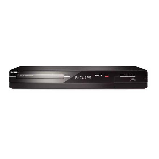
DVD Recorder
Service
Service
Service
Service
Service
Service Manual
c Copyright 2007 Philips Consumer Electronics B.V. Eindhoven, The Netherlands.
All rights reserved. No part of this publication may be reproduced, stored in a retrieval
system or transmitted, in any form or by any means, electronic, mechanical, photocopying,
or otherwise without the prior permission of Philips.
Published by FU-KC 0710 Service AV Systems
Version 1.1
All manuals and user guides at all-guides.com
3475
3475
Survey of versions:
/37
NTSC
Printed in The Netherlands
DVDR3475/
CLASS 1 LASER PRODUCT
KLASSE 1 LASER PRODUKT
KLASS 1 LASER APPARAT
CLASSE 1 PRODUIT LASER
Subject to modification
37
EN 3139 785 32511
Advertisement
Table of Contents

Related Manuals for Philips DVDR3475/37


Summary of Contents for Philips DVDR3475/37
- Page 1 KLASS 1 LASER APPARAT CLASSE 1 PRODUIT LASER c Copyright 2007 Philips Consumer Electronics B.V. Eindhoven, The Netherlands. All rights reserved. No part of this publication may be reproduced, stored in a retrieval system or transmitted, in any form or by any means, electronic, mechanical, photocopying, or otherwise without the prior permission of Philips.
-
Page 2: Table Of Contents
It also is important to understand that these CAUTIONS and NOTICES ARE NOT EXHAUSTIVE. Philips could not possibly know, evaluate and advice the service trade of all conceivable ways in which service might be done or of the possible hazardous consequences of each way. -
Page 3: Laser Beam Safety Precautions
All manuals and user guides at all-guides.com LASER BEAM SAFETY PRECAUTIONS This DVD player uses a pickup that emits a laser beam. Do not look directly at the laser beam coming from the pickup or allow it to strike against your skin. -
Page 4: Important Safety Precautions
All manuals and user guides at all-guides.com IMPORTANT SAFETY PRECAUTIONS Product Safety Notice K. When connecting or disconnecting the internal connectors, first, disconnect the AC plug from the Some electrical and mechanical parts have special AC outlet. safety-related characteristics which are often not evident from visual inspection, nor can the protection they give necessarily be obtained by replacing them with components rated for higher voltage, wattage,... - Page 5 All manuals and user guides at all-guides.com Safety Check after Servicing Examine the area surrounding the repaired location for damage or deterioration. Observe that screws, parts, and wires have been returned to their original positions. Afterwards, do the following tests and confirm the specified values to verify compliance with safety standards.
-
Page 6: Standard Notes For Servicing
Due to lead-free technology some rules have to be respected by the workshop during a repair: Pin 1 • Use only lead-free solder alloy Philips SAC305 with order code 0622 149 00106. If lead-free solder- paste is required, please contact the manufacturer Instructions for Connectors of your solder-equipment. - Page 7 For repair of such sets nothing changes. • On our website www.atyourservice.ce.Philips.com you find more Fig. S-1-1 information to: • BGA-de-/soldering (+ baking instructions) 2. Remove the flat pack-IC with tweezers while •...
- Page 8 All manuals and user guides at all-guides.com 3. The flat pack-IC on the CBA is affixed with glue, so With Iron Wire: be careful not to break or damage the foil of each 1. Using desoldering braid, remove the solder from pin or the solder lands under the IC when all pins of the flat pack-IC.
- Page 9 All manuals and user guides at all-guides.com 2. Installation Instructions for Handling Semi- conductors 1. Using desoldering braid, remove the solder from the foil of each pin of the flat pack-IC on the CBA Electrostatic breakdown of the semi-conductors may so you can install a replacement flat pack-IC more occur due to a potential difference caused by easily.
-
Page 10: Function Indicator Symbols
All manuals and user guides at all-guides.com FUNCTION INDICATOR SYMBOLS Note: If an error occurs, a message with the error number appears on the screen. Recording Error Error message You cannot record on this disc as Power Calibration Area is full. Error No. - Page 11 All manuals and user guides at all-guides.com Error Message Solution Error Description Priority You cannot record on this disc as Power Calibration Area is Insert a new disc. PCA is Full. (in REC start) full. Release the finalizing for this This disc is already finalized.
-
Page 12: Operating Controls And Functions
All manuals and user guides at all-guides.com OPERATING CONTROLS AND FUNCTIONS 1-5-1 E7E4AIB... - Page 13 All manuals and user guides at all-guides.com 1-5-2 E7E4AIB...
-
Page 14: Signal Name Abbreviations
All manuals and user guides at all-guides.com SIGNAL NAME ABBREVIATIONS Signal Name Function Signal Name Function PWSW Power on Signal Output +5V-L +5V Power Supply Ready/Busy communication FIP Drive Power Supply Control Signal 1V2CONT +1.2V Power Supply Control Signal REC-LED Recording LED Control Signal Tuner Voltage Input Signal REG-CONT... -
Page 15: Cabinet Disassembly Instructions
All manuals and user guides at all-guides.com CABINET DISASSEMBLY INSTRUCTIONS 1. Disassembly Flowchart Note: (1) Identification (location) No. of parts in the figures This flowchart indicates the disassembly steps to gain (2) Name of the part access to item(s) to be serviced. When reassembling, (3) Figure Number for reference follow the steps in reverse order. - Page 16 All manuals and user guides at all-guides.com (S-6) (S-6) [4] Power SW CBA (S-2) [6] Power Supply CBA (L-1) CN1061 CN1060 Shield A (L-1) CN1063 (L-1) [3] SW CBA (L-2) (L-3) Fig. D4 (L-2) [2] Front Assembly Fig. D2 (S-10) (S-4) M-PCB Plate Earth (S-3)
- Page 17 All manuals and user guides at all-guides.com 3. How to Eject Manually Note: When rotating the gear, be careful not to damage the gear. 1. Remove the Top Cover. 2. Rotate the gear in the direction of the arrow manually as shown below until the tray descends. 3.
-
Page 18: How To Initialize The Dvd Recorder
All manuals and user guides at all-guides.com HOW TO INITIALIZE THE DVD RECORDER To put the program back at the factory-default, initialize the DVD recorder as the following procedure. 1. Turn the DVD recorder on. 2. Confirm that no disc is loaded or that the disc tray is open. -
Page 19: Firmware Renewal Mode
All manuals and user guides at all-guides.com FIRMWARE RENEWAL MODE 1. Turn the power on and remove the disc on the tray. 4. Select the firmware version pressing arrow buttons, then press [OK]. 2. To put the DVD recorder into version up mode, Fig. -
Page 20: Block Diagrams
All manuals and user guides at all-guides.com BLOCK DIAGRAMS System Control Block Diagram E7E4ABLS 1-10-1... - Page 21 All manuals and user guides at all-guides.com Digital Signal Process Block Diagram E7E4ABLD 1-10-2...
- Page 22 All manuals and user guides at all-guides.com Video Block Diagram TMDS SERIALIZER TMDS ENCODER HDCP CIPHER/ ENCRYPTOR CONTROLLER AUDIO TO DIGITAL SIGNAL PROCESS BLOCK DIAGRAM E7E4ABLV 1-10-3...
- Page 23 All manuals and user guides at all-guides.com Audio Block Diagram E7E4ABLA 1-10-4...
- Page 24 All manuals and user guides at all-guides.com Power Supply Block Diagram E7E4ABLP 1-10-5...
-
Page 25: Schematic Diagrams / Cba's
All manuals and user guides at all-guides.com SCHEMATIC DIAGRAMS / CBA’S Standard Notes Notes: 1. Do not use the part number shown on these WARNING drawings for ordering. The correct part number is shown in the parts list, and may be slightly Many electrical and mechanical parts in this chassis different or amended since these drawings were have special characteristics. - Page 26 All manuals and user guides at all-guides.com AV 1/5 Schematic Diagram Parts Location Guide Ref No. Position Ref No. Position CAPACITORS RESISTORS C1501 R1515 C1502 R1516 C1503 R1518 C1506 R1519 C1507 R1520 C1508 R1524 C1509 R1527 C1511 R1528 C1512 R1531 C1513 R1532 C1520...
- Page 27 All manuals and user guides at all-guides.com AV 1/5 Schematic Diagram * NOTE These components (IC1502, C1509) can be used in any models. “ “ = SMD PLAY mode (Unit: Volt) However, you cannot mix components under (2.5) REC mode Group A with the ones under Group B.
- Page 28 All manuals and user guides at all-guides.com AV 2/5 Schematic Diagram “ “ = SMD PLAY mode (Unit: Volt) (2.5) REC mode The same voltage for Indicates that the voltage both PLAY & REC modes is not consistent here. E7E4ASCAV2 1-11-4...
- Page 29 All manuals and user guides at all-guides.com AV 2/5 Schematic Diagram Parts Location Guide Ref No. Position Ref No. Position Ref No. Position CAPACITORS CAPACITORS RESISTORS C1101 C1810 R1113 C1102 C1811 R1114 CONNECTOR C1121 R1117 C1122 CN1101 R1120 DIODES C1123 R1121 C1124 D1301...
- Page 30 All manuals and user guides at all-guides.com AV 3/5 Schematic Diagram Parts Location Guide Ref No. Position Ref No. Position CAPACITORS TRANSISTORS C1171 Q1601 RESISTORS C1172 C1201 R1173 C1202 R1174 C1203 R1201 C1204 R1202 C1205 R1203 C1206 R1204 C1211 R1205 C1212 R1206 C1221...
- Page 31 All manuals and user guides at all-guides.com AV 3/5 Schematic Diagram “ “ = SMD PLAY mode (Unit: Volt) (2.5) REC mode The same voltage for Indicates that the voltage both PLAY & REC modes is not consistent here. E7E4ASCAV3 1-11-7...
- Page 32 All manuals and user guides at all-guides.com AV 4/5 Schematic Diagram “ “ = SMD PLAY mode (Unit: Volt) (2.5) REC mode The same voltage for Indicates that the voltage both PLAY & REC modes is not consistent here. AV 4/5 Schematic Diagram Parts Location Guide Ref No.
- Page 33 All manuals and user guides at all-guides.com AV 5/5 Schematic Diagram FL2001 MATRIX CHART “ “ = SMD PLAY mode (Unit: Volt) (2.5) REC mode The same voltage for Indicates that the voltage both PLAY & REC modes is not consistent here. BS CS DR DTV BS CS AV 5/5 Schematic Diagram...
- Page 34 All manuals and user guides at all-guides.com AV CBA Top View 1-11-10 BE7E2AF01011A...
- Page 35 All manuals and user guides at all-guides.com AV CBA Bottom View C1231 PLUS LEAD PIN 3 OF CN1101 PIN 5 OF CN1101 PIN 7 OF CN1101 PIN 9 OF CN1101 PIN 17 OF CN1101 PIN 3 OF CN1051 1-11-11 BE7E2AF01011A...
- Page 36 All manuals and user guides at all-guides.com AV CBA Parts Location Guide Ref No. Position Ref No. Position Ref No. Position Ref No. Position Ref No. Position Ref No. Position Ref No. Position CAPACITORS CAPACITORS CAPACITORS RESISTORS RESISTORS RESISTORS COILS C1053 C1335 C2004...
- Page 37 All manuals and user guides at all-guides.com Power Supply Schematic Diagram “ “ = SMD PLAY mode (Unit: Volt) CAUTION ! CAUTION ! (2.5) REC mode Fixed voltage (or Auto voltage selectable) power supply circuit is used in this unit. For continued protection against fire hazard, The same voltage for Indicates that the voltage...
- Page 38 All manuals and user guides at all-guides.com Power Supply CBA Top/Bottom View CAUTION ! Because a hot chassis ground is present in the power CAUTION ! Fixed voltage (or Auto voltage selectable) power supply circuit is used in this unit. supply circut, an isolation transformer must be used.
- Page 39 All manuals and user guides at all-guides.com SW & Power SW Schematic Diagram “ “ = SMD PLAY mode (Unit: Volt) (2.5) REC mode The same voltage for Indicates that the voltage both PLAY & REC modes is not consistent here. SW Schematic Diagram Parts Location Guide Ref No.
- Page 40 All manuals and user guides at all-guides.com SW CBA Top View Power SW CBA Top View SW CBA Parts Location Guide Ref No. Position CONNECTORS CN1062 CN1063 DIODE D1200 RESISTORS R3001 R3002 R3003 R3004 R3005 R3008 R3009 R3010 R3020 SWITCHES SW3005 SW3008 SW3009...
- Page 41 All manuals and user guides at all-guides.com DVD Main 1/7 Schematic Diagram “ “ = SMD PLAY mode (Unit: Volt) 1 NOTE: (2.5) REC mode The order of pins shown in this diagram is different from that of actual IC101. The same voltage for Indicates that the voltage IC101 is divided into six and shown as IC101 (1/6) ~ IC101 (6/6) in this DVD Main Schematic Diagram Section.
- Page 42 All manuals and user guides at all-guides.com DVD Main 2/7 Schematic Diagram “ “ = SMD PLAY mode (Unit: Volt) 1 NOTE: (2.5) REC mode The order of pins shown in this diagram is different from that of actual IC101. The same voltage for Indicates that the voltage IC101 is divided into six and shown as IC101 (1/6) ~ IC101 (6/6) in this DVD Main Schematic Diagram Section.
- Page 43 All manuals and user guides at all-guides.com DVD Main 3/7 Schematic Diagram “ “ = SMD PLAY mode (Unit: Volt) 1 NOTE: (2.5) REC mode The order of pins shown in this diagram is different from that of actual IC101. The same voltage for Indicates that the voltage IC101 is divided into six and shown as IC101 (1/6) ~ IC101 (6/6) in this DVD Main Schematic Diagram Section.
- Page 44 All manuals and user guides at all-guides.com DVD Main 4/7 Schematic Diagram “ “ = SMD PLAY mode (Unit: Volt) 1 NOTE: (2.5) REC mode The order of pins shown in this diagram is different from that of actual IC101. The same voltage for Indicates that the voltage IC101 is divided into six and shown as IC101 (1/6) ~ IC101 (6/6) in this DVD Main Schematic Diagram Section.
- Page 45 All manuals and user guides at all-guides.com DVD Main 5/7 Schematic Diagram “ “ = SMD PLAY mode (Unit: Volt) 1 NOTE: (2.5) REC mode The order of pins shown in this diagram is different from that of actual IC101. The same voltage for Indicates that the voltage IC101 is divided into six and shown as IC101 (1/6) ~ IC101 (6/6) in this DVD Main Schematic Diagram Section.
- Page 46 All manuals and user guides at all-guides.com DVD Main 6/7 Schematic Diagram “ “ = SMD PLAY mode (Unit: Volt) (2.5) REC mode The same voltage for Indicates that the voltage both PLAY & REC modes is not consistent here. E7E4ASCD6 1-11-22...
- Page 47 All manuals and user guides at all-guides.com DVD Main 7/7 Schematic Diagram “ “ = SMD PLAY mode (Unit: Volt) 1 NOTE: (2.5) REC mode The order of pins shown in this diagram is different from that of actual IC101. The same voltage for Indicates that the voltage IC101 is divided into six and shown as IC101 (1/6) ~ IC101 (6/6) in this DVD Main Schematic Diagram Section.
- Page 48 All manuals and user guides at all-guides.com DVD Main CBA Top View 1-11-24 BE7H70G04021...
- Page 49 All manuals and user guides at all-guides.com DVD Main CBA Bottom View 1-11-25 BE7H70G04021...
-
Page 50: Waveforms
All manuals and user guides at all-guides.com WAVEFORMS Pin 7 of CN1101 Pin 5 of CN1101 VIDEO-Y 0.2V 20µsec VIDEO-Cr 0.2V 20µsec Pin 9 of CN1101 Pin 17 of CN1101 VIDEO-C 0.2V 20µsec AUDIO(L)-OUT 0.5ms C1231 PLUS LEAD Pin 3 of CN1051 VIDEO-CVBS 0.5V 20µsec... -
Page 51: Wiring Diagram
All manuals and user guides at all-guides.com WIRING DIAGRAM NTPA 1394 CABLE (W1) NTPB JW002 SUB-RXD FCS(+) FOCUS FCS(-) ACTUATOR SUB-TXD TRK(+) TRACKING TRK(-) SYS-RESET ACTUATOR SUB-SCLK TILT(+) TILT TILT(-) ACTUATOR LDD-IIN4 LDD-IIN3 VIDEO-C-IN LDD-IIN2 LDD-IINR VIDEO-Y/CVBS-IN 20 AUDIO+5V LDD-VDD DVD-LD DVD-AUDIO-MUTE 18 LDD-VDD... -
Page 52: System Control Timing Charts
All manuals and user guides at all-guides.com SYSTEM CONTROL TIMING CHARTS [ Tray Open ] Push Close Power on button is pressed. Tray insertion INNER-SW open? Tray insertion INNER-SW open? Tray ejection To disc distinction [ Tray Open ] button is pressed. INNER-SW open? SLED... - Page 53 All manuals and user guides at all-guides.com Parameter V*: Voltage T*: Event timer V0: 2.40 V T1: 0.050 s V1: 4.25 V T2: 2.000 s V2: 2.00 V T3: 0.008 s V3: 2.36 V T4: 0.006 s V4: 4.26 V T5: 0.066 s T6: 1.500 s T7: 0.800 s...
- Page 54 All manuals and user guides at all-guides.com Push close Threshold level 0.08 V 0.02 s Push Close detection 1-14-3 R4NTI...
-
Page 55: Ic Pin Function Descriptions
All manuals and user guides at all-guides.com IC PIN FUNCTION DESCRIPTIONS IC1501 (SUB MICRO CONTROLLER) Signal Function Name Signal Function FLASH- Name Serial Data Signal for Flash IN KEY-1 Key Data Input 1 FLASH- 36 OUT Serial Clock Signal for Flash IN KEY-2 Key Data Input 2 IN POW-SW... - Page 56 All manuals and user guides at all-guides.com IC2001 (VFD DRIVER) Signal Function Name IN CLK Serial Clock IN STB Serial Interface Strobe Not Used Not Used Power Supply Segment Output Pull Down Level 16 OUT i Segment Output Grid Output Power Supply IN OSC Oscillator Input...
-
Page 57: Lead Identifications
All manuals and user guides at all-guides.com LEAD IDENTIFICATIONS KRC103M-AT/P 2SA950-Y(TE2 F T) UTC4558 2SK3757(Q) KTA1267-(GR,Y)-AT/P 2SA1015-GR(TE2 F T) KIA4558P/P FQPF3N50C KTC3199-(BL,GR)-AT/P 2SC1815-(BL,GR)(TE2 F T) RN1203(TE4 F T) 2SC2120-Y(TE2 F T) KTA-1266-(GR,Y)-AT/P KTA1271-Y-AT/P KTC3203-Y-AT/P G D S E C B E C B MM1697AJBE MM1636XWRE... -
Page 58: Electrical Parts List
All manuals and user guides at all-guides.com ELECTRICAL PARTS LIST PRODUCT SAFETY NOTE: Products marked with a # have special characteristics important to safety. ELECTRICAL PARTS LIST Before replacing any of these components, read carefully the product safety notice in this service Pos.No. - Page 59 All manuals and user guides at all-guides.com ELECTRICAL PARTS LIST ELECTRICAL PARTS LIST Pos.No. # 12 NC Description Pos.No. # 12 NC Description CHIP CERAMIC CAP .(1608) F Z IC1502 9965 100 03070 SYSTEM RESET PST3619NR C1306 0.1UF/50V CHIP CERAMIC CAP .(1608) F Z C1511 CHIP CERAMIC CAP .(1608) B K 0.1UF/50V...
- Page 60 All manuals and user guides at all-guides.com ELECTRICAL PARTS LIST ELECTRICAL PARTS LIST Pos.No. # 12 NC Description Pos.No. # 12 NC Description D1065 PCB JUMPER D0.6-P10.0 IC1502 9965 100 03070 SYSTEM RESET PST3619NR D1070 SWITCHING DIODE 1SS133(T-77) CHIP CERAMIC CAP .(1608) B K C1509 0.1UF/25V D1070...
- Page 61 All manuals and user guides at all-guides.com ELECTRICAL PARTS LIST ELECTRICAL PARTS LIST Pos.No. # 12 NC Description Pos.No. # 12 NC Description Q1501 TRANSISTOR KTA1266-Y-AT/P R1104 RES CHIP 1608 1/10W F 68.0K OHM Q1501 TRANSISTOR 2SA1015-Y(TE2 F T) R1107 CHIP RES.
- Page 62 All manuals and user guides at all-guides.com ELECTRICAL PARTS LIST ELECTRICAL PARTS LIST Pos.No. # 12 NC Description Pos.No. # 12 NC Description R1226 RES CHIP 1608 1/10W J 1.0K OHM R1424 CARBON RES. 1/4W J 75 OHM R1232 CHIP RES. 1/10W J 100K OHM R1430 CARBON RES.
- Page 63 All manuals and user guides at all-guides.com ELECTRICAL PARTS LIST ELECTRICAL PARTS LIST Pos.No. # 12 NC Description Pos.No. # 12 NC Description R1565 CHIP RES. 1/10W J 47K OHM SW3011 TACT SWITCH SKQSAF001A R1565 RES CHIP 1608 1/10W J 47K OHM SW3011 TACT SWITCH KSM0614B R1571...
- Page 64 All manuals and user guides at all-guides.com ELECTRICAL PARTS LIST ELECTRICAL PARTS LIST Pos.No. # 12 NC Description Pos.No. # 12 NC Description D1002 DIODE 1N5397-B POWER INDUCTORS TWKBNP- L1052 180K D1002 DIODE 1N5397BD L1052 CHOKE COIL(18UH) LHL10NB180K D1003 DIODE 1N5397-B TRANSISTORS D1003 DIODE 1N5397BD...
- Page 65 All manuals and user guides at all-guides.com ELECTRICAL PARTS LIST Pos.No. # 12 NC Description DIODE D1200 LED(RED) 204HD/E RESISTORS R3001 CHIP RES. 1/10W J 300 OHM R3001 RES CHIP 1608 1/10W J 300 OHM R3002 CHIP RES. 1/10W J 620 OHM R3002 RES CHIP 1608 1/10W J 620 OHM R3003...
-
Page 66: Exploded Views
All manuals and user guides at all-guides.com EXPLODED VIEWS Cabinet 2L010 See Electrical Parts List for parts with this mark. Some Ref. Numbers are not in sequence. 2L010 2L030 2B49 2L050 2L041 2L050 2B10 2L010 ASSY 2b POWER SUPPLY CBA 2L040 ASSY 1 ASSY 2a... - Page 67 All manuals and user guides at all-guides.com Packing Lower Side Upper Side X20A X20B X20C X22A X22B X22C Unit Some Ref. Numbers are not in sequence. 1-18-2 E7E4APEX...
-
Page 68: Mechanical Parts List
All manuals and user guides at all-guides.com MECHANICAL PARTS LIST PRODUCT SAFETY NOTE: Products marked with a # have special characteristics important to safety. MECHANICAL PARTS LIST Before replacing any of these components, read carefully the product safety notice in this service manual. -
Page 69: Revision List
All manuals and user guides at all-guides.com REVISION LIST Version 1.0 * Initial release Version 1.1 * Addition of 12NC 1-20-1 E7E4AREV...
Need help?
Do you have a question about the DVDR3475/37 and is the answer not in the manual?
Questions and answers