Table of Contents
Advertisement
Quick Links
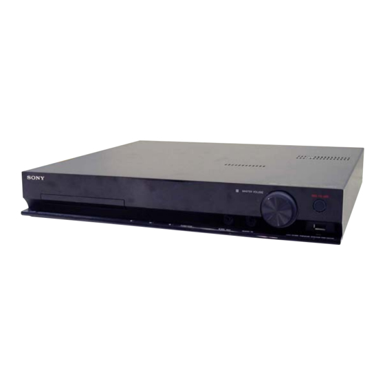
HBD-DZ330/DZ710/DZ730
SERVICE MANUAL
Ver. 1.0 2010.03
• HBD-DZ330/DZ710/DZ730 are the amplifi er, DVD/CD and
tuner section in DAV-DZ330/DZ710/DZ730.
This system incorporates with Dolby* Digital and Dolby Pro Logic (II)
adaptive matrix surround decoder and the DTS** Digital Surround System.
* Manufactured under license from Dolby Laboratories.
Dolby, Pro Logic, and the double-D symbol are trademarks of Dolby
Laboratories.
** Manufactured under license under U.S. Patent #'s:
5,451,942; 5,956,674; 5,974,380; 5,978,762; 6,487,535 & other U.S. and
worldwide patents issued & pending. DTS and DTS Digital Surround
are registered trademarks and the DTS logos and Symbol are trademarks
of DTS, Inc. © 1996-2008 DTS, Inc. All Rights Reserved.
Amplifi er Section
(DAV-DZ330/DAV-DZ730)
POWER OUTPUT (rated):
Front L + Front R
108 W + 108 W (at 3 ohms,
1 kHz, 1% THD)
POWER OUTPUT (reference):
Front L/Front R/Center/
Surround L/Surround R:
167 watts (per channel at 3
ohms, 1 kHz)
Subwoofer: 165 watts (at 3
ohms, 80 Hz)
Inputs (Analog)
TV (AUDIO IN)
Sensitivity: 450/250 mV
AUDIO IN
Sensitivity: 250/125 mV
Inputs (Digital)
TV (Audio Return Channel/OPTICAL IN)
Input Stream: Dolby
Digital 5.1ch/DTS 5.1ch/
Linear PCM 2ch
(Sampling Frequency: less
than 48 kHz)
Sony Corporation
9-889-805-01
2010C04-1
Audio&Video Business Group
©
2010.03
Published by Sony Techno Create Corporation
Model Name Using Similar Mechanism
Mechanism Type
Optical Pick-up Name
SPECIFICATIONS
Amplifi er Section
(DAV-DZ710)
POWER OUTPUT (rated):
Front L + Front R
108 W + 108 W (at 3 ohms,
1 kHz, 1% THD)
POWER OUTPUT (reference)
Front L/Front R/Center/
Surround L/Surround R:
167 watts (per channel at 3
ohms, 1 kHz)
Subwoofer: 165 watts (at 3
ohms, 80 Hz)
Inputs (Analog)
TV (AUDIO IN)
Sensitivity: 450/250 mV
MIC1
Sensitivity: 1 mV
MIC2
Sensitivity: 1 mV
Inputs (Digital)
TV (Audio Return Channel/OPTICAL IN)
Input Stream: Dolby
Digital 5.1ch/DTS 5.1ch/
Linear PCM 2ch
(Sampling Frequency: less
than 48 kHz)
AEP Model
HBD-DZ330/DZ730
UK Model
HBD-DZ330
Russian Model
HBD-DZ710
HBD-DZ170/DZ171/
DZ175/DZ310/DZ510/
DZ610/DZ810
CDM85MB-DVBU102
KHM-313CAA
Super Audio CD/DVD System
Laser Diode Properties
Emission Duration:
Continuous
Laser Output: Less than
44.6 μW
* This output is the value measurement at a distance
of 200 mm from the objective lens surface on the
Optical Pick-up Block with 7 mm aperture.
Signal format system
PAL/NTSC
USB Section
(USB) port:
Maximum current:
500 mA
Tuner Section
System
PLL quartz-locked digital
synthesizer
Tuning range
North American models: 87.5 MHz - 108.0 MHz
(100 kHz step)
Other models:
87.5 MHz - 108.0 MHz (50
kHz step)
Antenna (aerial)
FM wire antenna (aerial)
Antenna (aerial) terminals 75 ohms, unbalanced
Intermediate frequency
10.7 MHz
– Continued on next page –
DVD RECEIVER
Advertisement
Table of Contents


Need help?
Do you have a question about the HBD-DZ330 and is the answer not in the manual?
Questions and answers