Table of Contents
Advertisement
Quick Links
SERVICE MANUAL
Main Section
I Specifications
I Preparation for Servicing
I Adjustment Procedures
I Schematic Diagrams
I CBA's
I Exploded Views
I Parts List
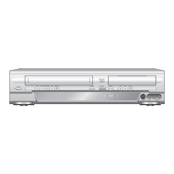
VIDEO CASSETTE RECORDER
POWER
DVD RECORDER &
EWR20V4
REW
F.FWD
STOP/EJECT
PLAY
RECORD
When servicing the deck
mechanism, refer to MK12.5 Deck
Mechanism Section.
Deck Mechanism Part No.:
N2260FL
OPEN/CLOSE
CHANNEL
DUBBING
SELECT
STOP
PLAY
RECORD
VCR
DVD
SELECT
S-VIDEO
VIDEO
L - AUDIO - R
Advertisement
Table of Contents

Related Manuals for Emerson EWR20V4


Summary of Contents for Emerson EWR20V4
- Page 1 I Preparation for Servicing Mechanism Section. I Adjustment Procedures I Schematic Diagrams I CBA’s Deck Mechanism Part No.: I Exploded Views N2260FL I Parts List DVD RECORDER & VIDEO CASSETTE RECORDER EWR20V4 OPEN/CLOSE F.FWD STOP/EJECT PLAY RECORD CHANNEL DUBBING SELECT STOP PLAY...
- Page 2 IMPORTANT SAFETY NOTICE Proper service and repair is important to the safe, reliable operation of all Funai Equipment. The service procedures recommended by Funai and described in this service manual are effective methods of performing service operations. Some of these service special tools should be used when and as recommended.
-
Page 3: Table Of Contents
MAIN SECTION DVD RECORDER & VIDEO CASSETTE RECORDER EWR20V4 Main Section I Specifications I Preparation for Servicing I Adjustment Procedures I Schematic Diagrams I CBA’s I Exploded Views I Parts List TABLE OF CONTENTS Specifications................1-1-1 Laser Beam Safety Precautions. -
Page 4: Specifications
SPECIFICATIONS < VCR Section > Description Unit Minimum Nominal Maximum Remark 1. Video 1-1. Video Output (PB) Vp-p SP Mode 1-2. Video Output (R/P) Vp-p SP Mode, 1-3. Video S/N Y (R/P) W/O Burst 1-4. Video Color S/N AM (R/P) SP Mode 1-5. - Page 5 < DVD Section > ITEM CONDITIONS UNIT NOMINAL LIMIT 1. VIDEO 1-1. Video Output 75 ohm load Vp-p 1-2. S-Video Output Y (Luminance) 75 ohm load Vp-p C (Chrominance) 75 ohm load Vp-p 0.286 1-3. Component Output Y (Luminance) 75 ohm load Vp-p Cb (Chrominance) 75 ohm load...
-
Page 6: Laser Beam Safety Precautions
LASER BEAM SAFETY PRECAUTIONS This DVD player uses a pickup that emits a laser beam. Do not look directly at the laser beam coming from the pickup or allow it to strike against your skin. The laser beam is emitted from the location shown in the figure. When checking the laser diode, be sure to keep your eyes at least 30cm away from the pickup lens when the diode is turned on. -
Page 7: Important Safety Precautions
IMPORTANT SAFETY PRECAUTIONS Product Safety Notice I. Also check areas surrounding repaired locations. J. Be careful that foreign objects (screws, solder Some electrical and mechanical parts have special droplets, etc.) do not remain inside the set. safety-related characteristics which are often not evi- K. - Page 8 Safety Check after Servicing Examine the area surrounding the repaired location for damage or deterioration. Observe that screws, parts, Chassis or Secondary Conductor and wires have been returned to their original posi- tions. Afterwards, do the following tests and confirm the specified values to verify compliance with safety Primary Circuit Terminals standards.
-
Page 9: Standard Notes For Servicing
STANDARD NOTES FOR SERVICING Circuit Board Indications Pb (Lead) Free Solder When soldering, be sure to use the Pb free solder. 1. The output pin of the 3 pin Regulator ICs is indi- cated as shown. How to Remove / Install Flat Pack-IC Top View Bottom View 1. - Page 10 3. The flat pack-IC on the CBA is affixed with glue, so With Soldering Iron: be careful not to break or damage the foil of each (1) Using desoldering braid, remove the solder from all pin or the solder lands under the IC when removing pins of the flat pack-IC.
- Page 11 2. Installation With Iron Wire: (1) Using desoldering braid, remove the solder from all (1) Using desoldering braid, remove the solder from pins of the flat pack-IC. When you use solder flux the foil of each pin of the flat pack-IC on the CBA so which is applied to all pins of the flat pack-IC, you you can install a replacement flat pack-IC more can remove it easily.
- Page 12 Instructions for Handling Semi-conductors Electrostatic breakdown of the semi-conductors may occur due to a potential difference caused by electro- static charge during unpacking or repair work. 1. Ground for Human Body Be sure to wear a grounding band (1MΩ) that is prop- erly grounded to remove any static electricity that may be charged on the body.
-
Page 13: Preparation For Servicing
PREPARATION FOR SERVICING How to Enter the Service Mode About Optical Sensors Caution: An optical sensor system is used for the Tape Start and End Sensors on this equipment. Carefully read and follow the instructions below. Otherwise the unit may operate erratically. What to do for preparation Insert a tape into the Deck Mechanism Assembly and press the PLAY button. -
Page 14: Operating Controls And Functions
OPERATING CONTROLS AND FUNCTIONS 1-6-1 E9400IB... - Page 15 1-6-2 E9400IB...
-
Page 16: Cabinet Disassembly Instructions
CABINET DISASSEMBLY INSTRUCTIONS 1. Disassembly Flowchart REMOVAL REMOVE/*UNHOOK/ This flowchart indicates the disassembly steps to gain LOC. PART Fig. UNLOCK/RELEASE/ Note access to item(s) to be serviced. When reassembling, UNPLUG/DESOLDER follow the steps in reverse order. Bend, route, and dress the cables as they were originally. DVD BE 4(S-6), *CN201, Main CBA... - Page 17 *=Unhook, Unlock, Release, Unplug, or Desolder e.g. 6(S-1) = six Screws (S-1), 5(L-1) = five Locking Tabs (L-1) (S-2) [4] Radiation Sheet (5): Refer to “Reference Notes.” (S-2) Reference Notes [3] Front (S-3) CAUTION 1: Locking Tabs (L-1) and (L-2) are fragile. Bracket Be careful not to break them.
- Page 18 (S-9) [9] FFC Friction Plate (S-5B) (S-5A) (S-10) (S-7) (S-8) (S-7) [10] Rear (S-9) Panel Unit [7] DVD (S-6) Mecha (S-6) & F/E (S-9) Assembly CN1606 [8] DVD BE CN1608 Main CBA Unit Fig. D5 [14] Rear Panel CN1604 (S-13) (S-12) CN201 CN202...
- Page 19 (S-17) (S-16) (S-17) (S-16) (S-16) (S-17) (S-18) [15] Bracket L (S-17) (S-14) (S-19) (S-15) [17] VCR (S-17) Chassis Unit [16] Bracket R Fig. D7 1-7-4 E9400DC...
- Page 20 Cylinder Assembly FE Head ACE Head Assembly SW512 LD-SW [18] Deck Assembly [19] Power SW CBA [20] Function [21] Main CBA [18] Deck Assembly (S-20) Cam Gear [21] Main Hole Lead Shaft with (S-21) blue Desolder stripe Hole LD-SW [21] Main CBA Desolder Lead with blue stripe...
- Page 21 (S-22) (S-22) [22] Deck Pedestal [23] Front Bracket R (S-23) Fig. D9 HOW TO EJECT MANUALLY 1. Remove the Top Cover. 2. Remove the Front Assembly. 3. Push the lever to the direction of the arrow as shown below. View for A Push the lever to the direction of the arrow Lever...
-
Page 22: How To Initialize The Dvd Recorder
HOW TO INITIALIZE THE DVD RECORDER To put the program back at the factory-default, initialize the DVD recorder as the following procedure. 1. Turn the DVD recorder on. 2. Confirm that no disc is loaded or that the disc tray is open. -
Page 23: Electrical Adjustment Instructions
ELECTRICAL ADJUSTMENT INSTRUCTIONS General Note: "CBA" is an abbreviation for "Circuit Board Assembly." NOTE: Figure 1 1.Electrical adjustments are required after replacing circuit components and certain mechanical parts. It is important to do these adjustments only after EXT. Syncronize Trigger Point all repairs and replacements have been com- pleted. -
Page 24: Firmware Renewal Mode
FIRMWARE RENEWAL MODE 1. Turn the power on and remove the disc on the tray. 4. Select the firmware version using arrow buttons, 2. To put the DVD recorder into version up mode, then press [ENTER] button on the remote control press [CM SKIP], [6], [5], and [4] buttons on the unit. -
Page 25: Block Diagrams
BLOCK DIAGRAMS Servo / System Control Block Diagram 1-10-1 E9400BLS... - Page 26 Sub System Control Block Diagram 1-10-2 E9400BLSUB...
- Page 27 Digital Signal Process Block Diagram 1-10-3 E9400BLD...
- Page 28 Video Block Diagram 1-10-4 E9400BLV...
- Page 29 Video Input Select Block Diagram 1-10-5 E9400BLVIS...
- Page 30 Video Output Select Block Diagram 1-10-6 E9400BLVOS...
- Page 31 Audio Block Diagram E9400BLA 1-10-7...
- Page 32 Audio Input/Output Select Block Diagram 1-10-8 E9400BLAS...
- Page 33 Hi-Fi Audio Block Diagram E9400BLH 1-10-9...
- Page 34 Power Supply Block Diagram 1-10-10 E9400BLP...
-
Page 35: Function Indicator Symbols
FUNCTION INDICATOR SYMBOLS < VCR Section > Note: The following symbols will appear on the indicator panel to indicate the current mode or operation of the VCR. On-screen modes will also be momentarily displayed on the tv screen when you press the operation buttons. Led Mode Indicator Active When reel and capstan mechanism is not... - Page 36 < DVD Section > Note: If an error occurs, a message with the error number appears on the screen. Recording Error Error message You cannot record on the disc as Power Calibration Area is full. Error No. Error Message Solution Error Description Priority An error occurs during data reading.
- Page 37 Error Message Solution Error Description Priority This program is not recordable Set "DVD-RW Recording During the CGMS picture (possible a in Video mode. Format" to "VR mode". record once) input. (Video Format Disc) During the CGMS picture (possible a This program is not allowed to Insert a ver.1.1 CPRM record once) input.
-
Page 38: Schematic Diagrams / Cba's And Test Points
SCHEMATIC DIAGRAMS / CBA’S AND TEST POINTS Standard Notes WARNING Many electrical and mechanical parts in this chassis have special characteristics. These characteristics often pass unnoticed and the protection afforded by them cannot necessarily be obtained by using replace- ment components rated for higher voltage, wattage, etc. - Page 39 LIST OF CAUTION, NOTES, AND SYMBOLS USED IN THE SCHEMATIC DIAGRAMS ON THE FOLLOWING PAGES: 1. CAUTION: FOR CONTINUED PROTECTION AGAINST FIRE HAZARD, REPLACE ONLY WITH THE SAME TYPE FUSE. ATTENTION: POUR UNE PROTECTION CONTINUE LES RISQES D'INCELE N'UTILISER QUE DES FUSIBLE DE MEMO TYPE.
- Page 40 Main 1/8 Schematic Diagram < VCR Section > REC VIDEO SIGNAL PB VIDEO SIGNAL REC AUDIO SIGNAL PB AUDIO SIGNAL MAIN 1/8 Ref No. Position IC501 TRANSISTORS Q501 Q502 Q506 CONNECTORS CN502 CN504 VARIABLE RESISTOR VR501 TEST POINTS TP505 TP513 1-11-3 1-11-4 E9400SCM1...
- Page 41 Main 2/8, Power SW & Sensor Schematic Diagram < VCR Section > FIP502 MATRIX CHART P.SCAN VCD VCR REPEAT VCD VCR XP SP LP EP P.SCAN REPEAT MAIN 2/8 Ref No. Position IC571 TRANSISTORS Q561 Q562 Q564 CONNECTORS CN1613 TEST POINTS TP502 TP506 TP507...
- Page 42 Main 3/8 Schematic Diagram < VCR Section > REC VIDEO SIGNAL PB VIDEO SIGNAL REC AUDIO SIGNAL PB AUDIO SIGNAL MAIN 3/8 Ref No. Position IC301 TRANSISTORS Q301 Q302 Q303 Q421 Q422 Q425 Q426 CONNECTOR CN253 TEST POINTS TP301 TP302 1-11-7 1-11-8 E9400SCM3...
- Page 43 Main 4/8 Schematic Diagram < VCR Section > PB Audio Signal REC Audio Signal 1-11-9 1-11-10 E9400SCM4...
- Page 44 Main 5/8 & Function Schematic Diagram < VCR Section > MAIN 5/8 Ref No. Position IC200 IC201 BB-2 TRANSISTORS Q202 BB-2 Q203 BB-1 CONNECTORS CN200 CC-2 CN1615 TEST POINTS TP200 TP201 TP202 TP203 1-11-11 1-11-12 E9400SCM5...
- Page 45 Main 6/8 Schematic Diagram < VCR Section > REC VIDEO SIGNAL PB VIDEO SIGNAL REC AUDIO SIGNAL PB AUDIO SIGNAL MAIN 6/8 Ref No. Position IC800 EE-2 IC801 GG-2 IC802 GG-1 IC803 HH-1 IC805 EE-3 IC900 FF-3 TRANSISTORS Q200 GG-1 Q201 GG-1 Q800...
- Page 46 Main 7/8 Schematic Diagram < VCR Section > REC VIDEO SIGNAL PB VIDEO SIGNAL REC AUDIO SIGNAL PB AUDIO SIGNAL REC Audio Signal (Digital) PB Audio Signal (Digital) MAIN 7/8 Ref No. Position IC804 KK-1 IC1405 LL-4 IC1406 LL-2 TRANSISTORS Q391 MM-2 Q802...
- Page 47 Main 8/8 Schematic Diagram < VCR Section > REC Audio Signal (Digital) PB Audio Signal (Digital) MAIN 8/8 Ref No. Position IC202 SS-4 IC203 SS-3 TRANSISTORS Q052 QQ-2 Q055 QQ-2 Q056 QQ-1 Q204 TT-2 Q1005 TT-2 Q1006 SS-2 Q1604 SS-3 CONNECTORS CN202 UU-4...
- Page 48 Power Supply Schematic Diagram < VCR Section > CAUTION FOR CONTINUED PROTECTION AGAINST FIRE HAZARD, REPLACE ONLY WITH THE SAME TYPE FUSE. NOTE : CAUTION ! ATTENTION : POUR UNE PROTECTION CONTINUE LES RISQES The voltage for parts in hot circuit is measured using Fixed voltage ( or Auto voltage selectable ) power supply circuit is used in this unit.
- Page 49 Jack Schematic Diagram < VCR Section > REC Video Signal (Analog) REC Audio Signal (Analog) 1-11-21 1-11-22 E9400SCJK...
- Page 50 DVD FE Main 1/4 Schematic Diagram < DVD Section > REC Video+Audio Signal (Digital) PB Video+Audio Signal (Digital) DVD FE MAIN 1/4 Ref No. Position IC5101 IC5103 IC5202 TRANSISTORS Q5101 Q5201 CONNECTOR CN5101 E9400SCFM1 1-11-23 1-11-24...
- Page 51 DVD FE Main 2/4 Schematic Diagram < DVD Section > REC Video+Audio Signal (Digital) PB Video+Audio Signal (Digital) DVD FE MAIN 2/4 Ref No. Position IC5301 IC5804 TRANSISTORS Q5301 Q5302 Q5802 CONNECTOR CN5301 1-11-25 1-11-26 E9400SCFM2...
- Page 52 DVD FE Main 3/4 Schematic Diagram < DVD Section > DVD FE MAIN 3/4 Ref No. Position IC5401 IC5501 IC5503 IC5601 IC5805 IC5806 CONNECTORS CN5501 CN5502B CN5603 CN5603B CN5801 1-11-27 1-11-28 E9400SCFM3...
- Page 53 DVD FE Main 4/4 Schematic Diagram < DVD Section > DVD FE MAIN 4/4 Ref No. Position IC5701 IC5703 IC5704 IC5705 IC5706 IC5707 CONNECTORS CN5701 CN5602B E9400SCFM4 1-11-29 1-11-30...
- Page 54 DVD BE Main 1/4 Schematic Diagram < DVD Section > REC Video+Audio Signal (Digital) PB Video+Audio Signal (Digital) *1 Note: REC Video Signal (Digital) REC Audio Signal (Digital) PB Video Signal (Digital) PB Audio Signal (Digital) 1. The order of pins shown are different from that of IC3 itself. 2.
- Page 55 DVD BE Main 2/4 Schematic Diagram < DVD Section > *1 Note: 1. The order of pins shown are different from that of IC3 itself. 2. IC3 is shown as IC3(1/6) through IC3(6/6) in DVD BE Main Schematic Diagram section. DVD BE MAIN 2/4 Ref No.
- Page 56 DVD BE Main 3/4 Schematic Diagram < DVD Section > *1 Note: 1. The order of pins shown are different from that of IC3 itself. 2. IC3 is shown as IC3(1/6) through IC3(6/6) in DVD BE Main Schematic Diagram section. DVD BE MAIN 3/4 Ref No.
- Page 57 DVD BE Main 4/4 Schematic Diagram < DVD Section > *1 Note: REC Video+Audio Signal (Digital) PB Video+Audio Signal (Digital) 1. The order of pins shown are different from that of IC3 itself. 2. IC3 is shown as IC3(1/6) through IC3(6/6) in DVD BE Main Schematic Diagram section. DVD BE MAIN 4/4 Ref No.
- Page 58 Main CBA Top View Sensor CBA Top View TP751 V-OUT TO SENSOR CBA BHB300F01014A (START-SENSOR) BHB300F01014B TO SENSOR CBA (END-SENSOR) TP301 C-PB TP302 RF-SW VR501 SW-P TP513 TP502 S-INH 1-11-39 1-11-40 BE9400F01011A...
- Page 59 Main CBA Bottom View R1402 WF11 PIN 2 OF TU900 WF12 PIN 10 OF PIN 6 OF CN201 TU900 WF13 PIN 12 OF PIN 11 OF CN201 TU900 WF14 PIN 14 OF PIN 12 OF CN201 TU900 WF15 PIN 18 OF TU900 PIN 27 OF CN201...
- Page 60 Power Supply CBA Top View CAUTION FOR CONTINUED PROTECTION AGAINST FIRE HAZARD, CAUTION ! REPLACE ONLY WITH THE SAME TYPE FUSE. Fixed voltage ( or Auto voltage selectable ) power supply circuit is used in this unit. ATTENTION : POUR UNE PROTECTION CONTINUE LES RISQES If Main Fuse (F1001) is blown, check to see that all components in the power supply D'INCELE N'UTILISER QUE DES FUSIBLE DE MÊME TYPE.
- Page 61 Power Supply CBA Bottom View CAUTION ! CAUTION BECAUSE A HOT CHASSIS GROUND IS PRESENT IN THE POWER Fixed voltage ( or Auto voltage selectable ) power supply circuit is used in this unit. FOR CONTINUED PROTECTION AGAINST FIRE HAZARD, SUPPLY CIRCUIT , AN ISOLATION TRANSFORMER MUST BE USED.
- Page 62 Jack CBA Top View Jack CBA Bottom View Function CBA Top View Function CBA Bottom View BE9400F01011D BE9400F01011C Power SW CBA Top View Power SW CBA Bottom View Junction CBA Top View Junction CBA Bottom View BE9400F01011B BE9400F01021B 1-11-47 1-11-48...
-
Page 63: Waveforms
WAVEFORMS NOTE: Input: COLOR BAR SIGNAL (WITH 1KHz AUDIO SIGNAL) TP751 R1402 WF11 Pin 2 of TU701 V-OUT E-E 10 µ s 50mV x 10 VIDEO-CVBS 0.5V 20µs MOD-A 20mV x 10 0.2ms TP751 UPPER Pin 12 of CN201 Pin 6 of TU701 TP302 WF12 LOWER... -
Page 64: Wiring Diagram < Vcr Section
WIRING DIAGRAM < VCR SECTION > 1-13-1 E9400WI... -
Page 65: Wiring Diagram < Dvd Section
WIRING DIAGRAM < DVD SECTION > 1-13-2 E9400WID... -
Page 66: System Control Timing Charts
SYSTEM CONTROL TIMING CHARTS [ VCR Section ] Mode SW : LD-SW LD-SW Position detection A/D Input voltage Limit Symbol (Calculated voltage) 3.76V~4.50V (4.12V) 4.51V~5.00V (5.00V) 0.00V~0.25V (0.00V) 1.06V~1.50V (1.21V) 0.66V~1.05V (0.91V) 1.99V~2.60V (2.17V) 1.51V~1.98V (1.80V) 3.20V~3.75V (3.40V) 0.26V~0.65V (0.44V) 4.51V~5.00V (5.00V) 2.61V~3.19V... - Page 67 Still/Slow Control Frame Advance Timing Chart 1) SP Mode 18 RF-SW The first rise of RF-SW after a rise in F-AD signal F-AD (Internal Signal) "H" "H" "Z" C-DRIVE "L" "L" Stop detection (T2) Acceleration Detection (T1) Slow Tracking Value PB CTL Reversal Limit Value 20ms...
- Page 68 2) LP/SLP Mode 18 RF-SW The first rise of RF-SW after a rise in F-AD signal F-AD (Internal Signal) "H" "H" "Z" C-DRIVE "L" "L" Stop detection (T2) Acceleration Detection (T1) Slow Tracking Value PB CTL Reversal Limit Value 20ms 27 C-F/R 79 H-A-SW 78 ROTA...
- Page 69 EJECT ST-S/ END-S "OFF" CASS.LOAD LD-FWD 0.2S LD-REV 0.7S LD-FWD 0.4S LD-FWD 0.2S LD-REV 0.2S LD-FWD 0.5S LD-REV STOP(A) PLAY LD-FWD PLAY LD-FWD LD-REV 0.2S LD-FWD PLAY PLAY PAUSE (SLOW) LD-FWD STILL(SLOW) PLAY LD-REV 0.2S LD-FWD PLAY STOP /EJECT LD-REV STOP(A) Fig.
- Page 70 STOP(A) STOP STOP(A) STOP LD-REV LD-REV 0.2S 0.2S LD-FWD LD-FWD STOP STOP /EJECT /EJECT 1.0S 1.0S LD-FWD LD-FWD 0.5S 0.5S LD-REV LD-REV STOP(A) STOP(A) LD-REV LD-REV 0.2S 0.2S LD-FWD LD-FWD STOP STOP /EJECT LD-REV /EJECT LD-REV 1.0S 1.0S LD-FWD LD-FWD 0.5S 0.5S LD-REV...
- Page 71 [ DVD Section ] Tray in 5.0V Tray in 5.0V Tray out Sled Drive 1.35V Disc Drive 1.35V 1.35V Focus Drive 1.35V Tracking Drive Tray out 5.0V Tray in 5.0V Tray out 1.35V Sled Drive 1.35V Disc Drive 1.35V Focus Drive 1.35V Tracking Drive 1-14-6...
- Page 72 Spin up 5.0V Tray in 5.0V Tray out Sled Drive 1.35V Disc Drive 1.35V 1.35V Focus Drive 1.35V Tracking Drive Playing 5.0V Tray in 5.0V Tray out Sled Drive 1.35V Disc Drive 1.35V 1.35V Focus Drive 1.35V Tracking Drive 1-14-7 E9400TI...
-
Page 73: Ic Pin Function Descriptions
IC PIN FUNCTION DESCRIPTIONS [ VCR Section ] Signal Active Function Name Level IC501 ( SYSTEM CONTROL MICROPROCESOR ) System Reset Signal IN RESET “H” ≥ 4.5V, “L” ≤ 1.0V (Reset=”L”) 21 OUT LM-FWD/ Loading Motor FWD/ H/Z/L Signal Active REV Output Function Name... - Page 74 Signal Active Signal Active Function Function Name Level Name Level OUTPUT- Output Select N.U. Not Used 46 OUT SELECT (DVD=”L”/VCR=”H”) N.U. Not Used Drum PG/FG Input IN D-PFG PULSE N.U. Not Used Signal N.U. Not Used N.U. Not Used Color Phase Rotary Capstan Motor 78 OUT C-ROTA Changeover Signal...
- Page 75 Signal Signal Name Function Name Function Name Name Transmission Data to Main XCIN Sub Clock Input OUT SUB-TXD Micro Controller OUT XCOUT Sub Clock Output Reception Data from Main SUB-RXD Main Clock Input Micro Controller OUT XOUT Main Clock Output OUT SUB-SCL Serial Clock Ground...
- Page 76 [ DVD Section ] IC571 [ PT6313-S-TP ] Signal In/Out Name Function Name Clock Input Serial Interface Strobe N.U. Not Used N.U. Not Used Power Supply OUT a OUT b OUT c OUT d Segment Output OUT e OUT h Pull Down Level OUT i Segment Output...
-
Page 77: Lead Identifications
LEAD IDENTIFICATIONS BU4053BCF 2SA1175(J,H,F) 2SA1015-GR(TPE2) KIA4558P CD4053BCSJX 2SC2785(J,H,F,K) 2SC1815-GR(TPE2) NJM2100D TC4052BF(EL) BA1F4M-T 2SC1815-Y(TPE2) NJM4558D TC4053BF(N) BN1F4M-T 2SC2120-O-TPE2 KRA103M 2SC2120-Y(TPE2) KRC103M KTC3198(GR,Y) KRC108M KTC3203(O,Y) KTA1266(GR) KTA1267(GR,Y) KTC3193(Y) KTC3199(GR,Y) E C B E C B 2SA933AS(S) EL817A PQ070XF01SZ 2SK3563 S2Y52 2SC536NF-NPA-AT EL817B PT6313-S-TP 2SC536NG-NPA-AT EL817C... -
Page 78: Exploded Views
EXPLODED VIEWS Cabinet 2L011 2L011 2L071 See Electrical Parts List 2L071 2L071 for parts with this mark. AC1001 2L071 2L081 Some Ref. Numbers are 2L011 2L082 not in sequence. 2L062 2L044 2L100 FM1001 2L081 W005 2L044 2B10 2L018 2L044 Sensor CBA 2L033 2L011 2L045... - Page 79 Packing Some Ref. Numbers are not in sequence. Unit 1-17-3 E9400PEX...
-
Page 80: Mechanical Parts List
DRY BATTERY R6P/2S or XB0M451T0001 LABEL, BAR CODE E9400UD ---------- DRY BATTERY ES-GR6M-C XB0M571GLP01 LABEL, TELEPHONE NUMBER ---------- RF CABLE 2.5C-2V WPZ0901TM002 H7931UD(EMERSON) ACCESSORY BAG E5700UD 0VM415576 FOOT K7010UA 0VM403657 AV CORD TSCKA-Y/RW100 or WPZ0102TM015 DECK ASSEMBLY CZD013/VM2260 N2260FL AV CORD RCA(M*2)TO RCA(M*2) WPZ0102LTE01 DVD MECHA &... -
Page 81: Electrical Parts List
ELECTRICAL PARTS LIST PRODUCT SAFETY NOTE: Products marked with a Ref. No. Description Part No. # have special characteristics important to safety. C302 CHIP CERAMIC CAP . CH J 390pF/50V CHD1JJ3CH391 Before replacing any of these components, read care- C303 PCB JUMPER D0.6-P5.0 JW5.0T fully the product safety notice in this service manual. - Page 82 Ref. No. Description Part No. Ref. No. Description Part No. C438 ELECTROLYTIC CAP . 4.7µF/25V M H7 CE1EMAVSL4R7 C752 CHIP CERAMIC CAP . B K 1000pF/50V CHD1JK30B102 C439 ELECTROLYTIC CAP . 4.7µF/25V M H7 CE1EMAVSL4R7 C762 ELECTROLYTIC CAP . 4.7µF/50V M H7 CE1JMAVSL4R7 C440 ELECTROLYTIC CAP .
- Page 83 Ref. No. Description Part No. Ref. No. Description Part No. C917 CHIP CERAMIC CAP . B K 0.1µF/50V CHD1JK30B104 SWITCHING DIODE 1SS133(T-77) QDTZ001SS133 C918 CHIP CERAMIC CAP . B K 0.1µF/50V CHD1JK30B104 D205 SWITCHING DIODE 1N4148M or NDTZ01N4148M C919 ELECTROLYTIC CAP . 0.33µF/50V M H7 CE1JMAVSLR33 SWITCHING DIODE 1SS133(T-77) QDTZ001SS133...
- Page 84 Ref. No. Description Part No. Ref. No. Description Part No. L202 PCB JUMPER D0.6-P5.0 JW5.0T TRANSISTOR KTC3198(GR) or NQS40KTC3198 L251 PCB JUMPER D0.6-P5.0 JW5.0T TRANSISTOR 2SC536NF-NPA-AT or QQSFC536NNPA L303 INDUCTOR(100µH K) LAP02TA101K LLAXKATTU101 TRANSISTOR 2SC536NG-NPA-AT QQSGC536NNPA L304 CHOKE COIL 47µH-K or LLBD00PKV007 Q301 TRANSISTOR KTA1266(GR) or...
- Page 85 Ref. No. Description Part No. Ref. No. Description Part No. CHIP RES.(1608) 1/10W J 4.7k Ω TRANSISTOR KTC3198(GR) or NQS40KTC3198 R231 RRXAJR5Z0472 CHIP RES.(1608) 1/10W 0 Ω TRANSISTOR 2SC536NF-NPA-AT or QQSFC536NNPA R232 RRXAJR5Z0000 CHIP RES.(1608) 1/10W J 10M Ω TRANSISTOR 2SC536NG-NPA-AT QQSGC536NNPA R233 RRXAJR5Z0106...
- Page 86 Ref. No. Description Part No. Ref. No. Description Part No. CHIP RES.(1608) 1/10W J 39k Ω CHIP RES.(1608) 1/10W J 470 Ω R301 RRXAJR5Z0393 R470 RRXAJR5Z0471 CHIP RES.(1608) 1/10W J 3.3k Ω CHIP RES.(1608) 1/10W J 1k Ω R302 RRXAJR5Z0332 R471 RRXAJR5Z0102 CHIP RES.(1608) 1/10W J 1.2k Ω...
- Page 87 Ref. No. Description Part No. Ref. No. Description Part No. CHIP RES.(1608) 1/10W J 10k Ω CHIP RES.(1608) 1/10W 0 Ω R615 RRXAJR5Z0103 R900 RRXAJR5Z0000 CHIP RES.(1608) 1/10W J 10k Ω CHIP RES.(1608) 1/10W J 180k Ω R618 RRXAJR5Z0103 R902 RRXAJR5Z0184 CHIP RES.(1608) 1/10W J 10k Ω...
- Page 88 Ref. No. Description Part No. Ref. No. Description Part No. CARBON RES. 1/4W J 22 Ω R2092 RCX4JATZ0220 JK805 RCA JACK MSP-382V-12 PBSN JXRL020LY063 CARBON RES. 1/4W J 180 Ω R2098 RCX4JATZ0181 JK1202 RCA JACK(BLACK) MSP-281V2-B JXRL010LY062 CARBON RES. 1/4W J 82 Ω R2099 RCX4JATZ0820 JK1401...
- Page 89 Ref. No. Description Part No. Ref. No. Description Part No. FFC CABLE 8P FFC/P1.25/120 WX1E9400-013 ELECTROLYTIC CAP . 1000µF/6.3V M CE0KMASTL102 C021 ELECTROLYTIC CAP . 470µF/6.3V M or CE0KMASDL471 FUNCTION CBA ELECTROLYTIC CAP . 470µF/6.3V M CE0KMASTL471 C023 CERAMIC CAP . B K 470pF/100V CCD2AKS0B471 Ref.
- Page 90 Ref. No. Description Part No. Ref. No. Description Part No. CARBON RES. 1/4W J 680k Ω SWITCHING DIODE 1N4148M NDTZ01N4148M R1034 RCX4JATZ0684 CARBON RES. 1/6W J 1k Ω or D1025 SWITCHING DIODE 1SS133(T-77) or QDTZ001SS133 R1035 RCX6JATZ0102 CARBON RES. 1/4W J 1k Ω SWITCHING DIODE 1N4148M NDTZ01N4148M RCX4JATZ0102...
- Page 91 EWR20V4 E9400UD 2004-04-19...
Need help?
Do you have a question about the EWR20V4 and is the answer not in the manual?
Questions and answers