Advertisement
Quick Links
ASM-2 Construction Guide
ASM-2 Construction Notes
For PCB Rev 2.3
February 5, 2020
Please note that this document is still currently under revision and we apologise for any errors or omissions.
Readers should feel free to email any comments to me at the address given below.
ELBY Designs - Laurie Biddulph
9 Follan Close, Kariong, NSW 2250, Australia
elby-designs@bigpond.com
http://www.elby-designs.com
1 of 19
Advertisement

Related Manuals for Elby Designs ASM-2


Summary of Contents for Elby Designs ASM-2
- Page 1 Please note that this document is still currently under revision and we apologise for any errors or omissions. Readers should feel free to email any comments to me at the address given below. ELBY Designs - Laurie Biddulph 9 Follan Close, Kariong, NSW 2250, Australia elby-designs@bigpond.com...
- Page 2 We recommend you read our General Construction Notes for general assembly guidance and other useful information. ELBY Designs - Laurie Biddulph 9 Follan Close, Kariong, NSW 2250, Australia elby-designs@bigpond.com http://www.elby-designs.com 2 of 19...
- Page 3 ASM-2 Construction Guide General notes on the assembly of the ASM-2 PCB: All resistors on the PCB are on a 0.4” pitch whilst most diodes are on a 0.3” pitch and so these components can be generally preformed before insertion in to the pcb. Capacitors in the range 1nF to 1uF are normally on a 0.2”...
- Page 4 This is totally optional and only for those who are after perfect performance. ELBY Designs - Laurie Biddulph 9 Follan Close, Kariong, NSW 2250, Australia elby-designs@bigpond.com http://www.elby-designs.com...
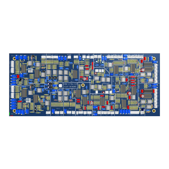
- Page 5 These components are NOT included in ASM2 Component Kit. A hard-copy of the component overlay can be printed using this ASM-2 PCB Overlay PDF file. It is sized for A3. 3D Model...
-
Page 6: Vco - Voltage Controlled Oscillator
3 and the shortened pin 4 - see image at right 3. Install the socket on to the pcb ensuring that there is a small gap between pin 4 of the socket and the pcb ELBY Designs - Laurie Biddulph 9 Follan Close, Kariong, NSW 2250, Australia elby-designs@bigpond.com http://www.elby-designs.com... - Page 7 3. Finally, using P106 (P156) adjust the output until is centered around 0V. Sine Waveform Adjustment 1. Monitor the Sine output on J102 (J152) and using P102 (P152) adjust the output for a peak-peak output of 10V. ELBY Designs - Laurie Biddulph 9 Follan Close, Kariong, NSW 2250, Australia elby-designs@bigpond.com http://www.elby-designs.com...
- Page 8 Now measure the voltage at the LP output. Set OFFSET 1 so that this voltage is as close to zero as you can get it. Again aim for +/-5mV or less. ELBY Designs - Laurie Biddulph 9 Follan Close, Kariong, NSW 2250, Australia elby-designs@bigpond.com...
- Page 9 Press a lower key and tune the filter manually to the VCO frequency again with P801 (Frequency). Press higher again adjust P802 zero beatings. Repeat this process a few times. ELBY Designs - Laurie Biddulph 9 Follan Close, Kariong, NSW 2250, Australia elby-designs@bigpond.com http://www.elby-designs.com 9 of 19...
- Page 10 P804 minimum resistance and P803 to the mid position. P807 should be set to its center position. ELBY Designs - Laurie Biddulph 9 Follan Close, Kariong, NSW 2250, Australia elby-designs@bigpond.com http://www.elby-designs.com 10 of 19...
- Page 11 5. Adjust P456 so that the rising edge of the envelope peaks at 5V0 and that there is no overshoot or undershoot. This completes the setting up for the ADSR 2 module. ATTACK PEAK Adjustment ELBY Designs - Laurie Biddulph 9 Follan Close, Kariong, NSW 2250, Australia elby-designs@bigpond.com http://www.elby-designs.com...
- Page 12 VCA (1)(2) - Voltage Controlled Amplifier Apply xV Monitor TP13 and adjust P301 for minimum output Monitor TP14 and adjust P351 for minimum output ELBY Designs - Laurie Biddulph 9 Follan Close, Kariong, NSW 2250, Australia elby-designs@bigpond.com http://www.elby-designs.com 12 of 19...
- Page 13 The white noise output should be between 2.0 and 2.8V peak-to-peak. Different transistors should be tested along with varying the value of P601. ELBY Designs - Laurie Biddulph 9 Follan Close, Kariong, NSW 2250, Australia elby-designs@bigpond.com http://www.elby-designs.com...
- Page 14 LED brightness should be at minimum brightness when the triangle is at its most negative, and at maximum brightness when the triangle is at its most positive. ELBY Designs - Laurie Biddulph 9 Follan Close, Kariong, NSW 2250, Australia elby-designs@bigpond.com...
- Page 15 ASM-2 Construction Guide Glide Buffer Power up, Testing and Calibration Procedures There is no calibration required for the GLIDE circuit ELBY Designs - Laurie Biddulph 9 Follan Close, Kariong, NSW 2250, Australia elby-designs@bigpond.com http://www.elby-designs.com 15 of 19...
-
Page 16: Ring Modulator
[CARRIER] input may be trimmed to between 10mV (-60dB) and 20mV (-54dB). For the [SIGNAL] input this will, typically, be between 40mV (-48dB) and 80mV (-42dB). ELBY Designs - Laurie Biddulph 9 Follan Close, Kariong, NSW 2250, Australia elby-designs@bigpond.com http://www.elby-designs.com... -
Page 17: Sample & Hold
The Sample & Hold circuit has a small pcb footprint error. C901 should be replaced with a resistor which can be simply stood on end to fit the board. Power up, Testing and Calibration Procedures ELBY Designs - Laurie Biddulph 9 Follan Close, Kariong, NSW 2250, Australia elby-designs@bigpond.com http://www.elby-designs.com... - Page 18 12V) Power up, Testing and Calibration Procedures 1. Monitor TP2 and adjust P1 (+7V) for +9.0V 2. Monitor TP3 and adjust P2 (-7V) for -9.0V ELBY Designs - Laurie Biddulph 9 Follan Close, Kariong, NSW 2250, Australia elby-designs@bigpond.com http://www.elby-designs.com 18 of 19...
- Page 19 ASM-2 Construction Guide MULTIPLES These are simple 1-in -to- 2-out passive multiples. ELBY Designs - Laurie Biddulph 9 Follan Close, Kariong, NSW 2250, Australia elby-designs@bigpond.com http://www.elby-designs.com 19 of 19...
Need help?
Do you have a question about the ASM-2 and is the answer not in the manual?
Questions and answers