Table of Contents
Advertisement
Quick Links
Advertisement
Table of Contents

Related Manuals for Tektronix 511A-AD


Summary of Contents for Tektronix 511A-AD
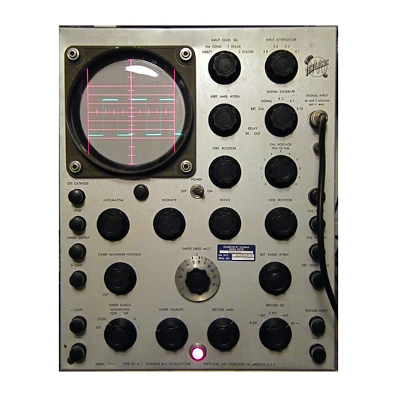
- Page 3 ATHODE-RAY OS ILLOS OPE TYPE 511A-AD SERIAL NUMBER _________________________ NSTRUCT ON MANUAL ANUFACTURERS OF CATHODE-RAY AND VIDEO TEST INSTRU ENTS Sunset Highway and Barnes Road • P.O.Box 831 • Portland 7, Oregon, U. S. A. Phone: Ypress 2-2611 • ables: Tektronix...
-
Page 5: Eneral Description
1 Stage, 2.7 V per cm maximum, 40 V per cm mini mum. The Tektronix Type 511-A Cathode Ray Oscillo 2 Stages, .27 V per cm maximum, 4 V per cm mini scope is a wide range, portable instrument, making mum. - Page 6 Potentiometer controlling the average PANEL MARKINGS EXPLANATION NTENS TY grid voltage of the CRT and thereby the brightness of the image. NPUT CHAN. Gang switch permitting the input SEL. signal to be connected to the vertical deflection plates either directly, via a POWER On-off switch in the AC line voltage .1 mfd capacitor, 1 stage amplifier, or...
- Page 7 - GATE Binding post for connection via .1 ca TR GGER SEL. Switch determining source and polari pacitor to the plate of (V8). This fur ty of trigger voltage. nishes a 40 V negative pulse of the same duration as the sweep.
- Page 9 AUTION — DO NOT ALLOW TH S SPOT SECT ON TO BE EXCESS VELY BR GHT OR RE MA N FOR LONG N ONE POS T ON. OPERATIN INSTRUCTIONS 6. Advance the SWEEP STAB L TY control until a sweep appears, then turn it back just under this point.
- Page 10 NOTE — When using the internal trigger im- Recurrent Sweep pulses to view fundamental frequencies n case it is desirable to have a sweep without using any sort of trigger, merely advance the SWEEP STAB L above about 2mc it will be necessary to TY control until a stable sweep is obtained.
- Page 11 creasing L6, and readjusting L7, L8, L9, and L 10 , but With the EXT. SWEEP ATTEN. fully clockwise the de overshoot will occur on steep wave fronts. With opti flection sensitivity is approximately 1.5 volts per cm DC mum transient response, the rise time (10% to 90% of or peak to peak AC.
-
Page 12: Sweep Output
ALIBRATION AUTION- DO NOT OVERLOAD THE AMPL F ERS WHEN MAK NG AMPL While the cathode ray oscilloscope is usually em TUDE MEASUREMENTS. ployed only as a qualitative rather than a quantitative device, it is the only instrument capable of making many types of voltage and current measurements on non sinusoidal wave shapes. - Page 13 FREQUEN Y TEKTRONIX JN . 12-28-50...
-
Page 15: Circuit Description
trigger amplifier V2 requires a positive impulse on its SECT ON grid to provide the correct trigger to the multivibrator. When the TR GGER SEL. switch is in the — NT. or +EXT. positions, signals are taken off the cathode of CIRCUIT DESCRIPTION V and do not change in polarity. - Page 16 GATE voltages available at the front panel binding period the 6AG7 tube V9 is held fully conducting since posts. The duration of the time V5 is cut off is deter it has no bias and therefore its plate is about at ground mined by the time constant of C7, R20C, R20C1 thru potential.
- Page 17 is turned to the OUT position which operates a SPDT VERTI AL DEFLE TION SYSTEM switch connecting the sweep amplifier directly to the The vertical deflection system provides the means of plate of the sweep generator. attenuating or amplifying input signal amplitudes so that they may present a convenient image on the cath ...
-
Page 18: Power Supply
The chassis of the Type 511 A is drilled to permit the insertion of a Tektronix Type 1AD25 Delay Network. This delays the signals .25 microseconds with POWER SUPPLY out appreciable distortion. - Page 19 the regulated +225 as reference voltage. Thus, if the put of the regulator, the reverse action takes place. +225 is not set ats its correct value, the +450 volt output Thus an equilibrium is reached where the regulated will also be in error. output voltage is held constant within very narrow limits.
-
Page 21: Maintenance And Adjustment
lar capacitors may drip if the instrument has been over SECT ON V heated by operating in a restricted space. This condition usually does not indicate replacement. Composition re sistors should be checked for serious discoloration, MAINTENANCE AND ADJUSTMENT which would indicate excessive dissipation and there ... - Page 22 may be used if available. This method is explained in measure the voltage between each CRT deflection plate detail under servicing instructions for each chassis. and ground, which should be within ±60 volts. The Since a large percentage of troubles experienced will average potential of both horizontal (X) plates, or both likely be caused by defective tubes, it is advisable to vertical (Y) plates, should be within ±40 volts of ground...
- Page 23 Sweep ircuits sweep speed), V9 is known to be good, and circuit volt ages appear normal, remove V9 and measure the volt Trouble in the sweep circuits is indicated when a spot age at terminal 4 of V9 socket, which should be between on the CRT screen can be obtained, but advancing the + 5 and +30 volts.
- Page 24 Connect a short wire between the CAL. OUTPUT and 2. C39, C51. These electrolytic capacitors are em the TR GGER NPUT binding posts, set the sweep speed ployed in the low frequency compensating circuits, and at 10,000 microseconds, the S GNAL CAL BRATE switch should be replaced if the range of R99 and R116 be ...
- Page 25 Voltage and Continuity Tables NPUT CHAN. SEL ......2 Stages NPUT ATTENUATOR ....X VERT. AMPL. ATTEN ....Clockwise S GNAL CAL BRATE ....Signal VERT. POS T ON ......Centered AUTION — THE POTENT ALS AND RE CAL. VOLTAGE ......0 S STANCES L STED N THESE TABLES AST GMAT SM ......
- Page 26 Tube Voltage ..10 volt scale Gnd. 1, 5 + . 5 2,3,7 Gnd. 6.5AC Gnd. V7.1- Gnd. +220 SWEEP STAB L TY clockwise 1, 7 Gnd. SWEEP STAB L TY counter clockwise A, B SWEEP STAB L TY clockwise ....50 volt scale Gnd.
- Page 27 Tube Voltage Gnd. 1,4,5 +450 V 15 pin 4 6.5AC Gnd. +230 to +390 depending on setting of R42 Gnd. 450 V S2C 2 in 1 microsec. pos. Gnd. +260 to +400 depending on setting of R42 Gnd. 440 V S2C 2 in 1 microsec.
- Page 28 Tube Voltage Pin 14 NTENS TY counter clockwise Gnd. -750 FOCUS clockwise Gnd. -1100 FOCUS counter clockwise Gnd. 0 (±40v) SWEEP STAB L TY counter clockwise — spot centered Gnd. 0 (±40v) Gnd. -140 AST GMAT SM clockwise Gnd. +225 AST GMAT SM counter clockwise Gnd.
- Page 29 POINT TO POINT TUBE SO KET ONTINUITY (Tubes in Sockets) NOTE: Readings less than .1 ohm are listed 0. Tube Pin No. Resistan c e Gnd. Gnd. Gnd. 1830 Gnd. 470K Gnd. 1830 +225 4.7K Gnd. +225 6.2K Gnd. Gnd. Gnd.
- Page 30 Tube Pin No. Resistance Gnd. Gnd. 250K Gnd. Gnd. Gnd. Gnd. -140 4-225 Gnd. +225 Gnd. Gnd. infinite Gnd. Gnd. +225 V9 pin 8 Gnd. V 11 +225 +225 14.7K Gnd. Gnd. Gnd. 8.2K SWEEP MAGN F ER POS T ON out Gnd.
- Page 31 Tube Pin No. Resistance V16.1 1 2, 6, 7 T 1 term. 16 Gnd. 20.55K S GNAL-CAL BRATE switch in S GNAL position Gnd. S GNAL-CAL BRATE switch in 100 v. position 4, 5 Gnd. Gnd. Gnd. 1,3,5 Gnd. Gnd. Gnd.
- Page 32 Resistance Tube Pin No. Gnd. 550K +225 T 1 , term. 22 T 1 , term. 23 V25 pin 1 +225 +450 130K V22 pin 8 470K +225 +225 Gnd. Gnd. Gnd. 630K with R-159 set at midpoint +225 Gnd. Gnd.
- Page 33 Waveform Photographs The following photographs are provided to facilitate 1. Loading effect of the test oscilloscope. servicing of the Type 511-A and will prove especially 2. Non-linearity of the test oscilloscope. useful if another oscilloscope is available to observe the waveforms of the circuits being tested.
- Page 34 POWER SUPPLY WAVEFORMS Fig. 5. 60 cycle ripple of — 140 volt rectifier output at Fig. 6. 120 cycle ripple of -225 volt rectifier output at V24 plate. Amplitude 12 volts. V22 cathode and +450 volt rectifier output at V21 cathode. Amplitude 15 volts. Fig.
- Page 35 Fig. 11. Multivibrator waveform at V5 grid, controls set Fig. 12. Multivibrator waveform at V5 plate, controls set for 10 µsec. recurrent sweep. Amplitude 85 volts. for 10 µsec. recurrent sweep. Amplitude 160 volts. Fig. 13. Waveform at + GATE, controls set for 1000 µsec. Fig.
- Page 36 Fig. 22. Magnified sweep waveform at V 1 1 plate, show Fig. 21. Sweep sawtooth at V9 plate, 10 µsec . recurrent ing the 10 µsec . recurrent sweep of Fig. 20 mag sweep. Amplitude 35 volts. This waveform also nified 5X.
- Page 37 VIDEO AMPLIFIER WAVEFORMS These photographs should be used in conjunction with the Adjustment section of this manual during ad justment of the video amplifier. Fig. 30. Response to 50 cycle square wave when low frequency compensation is excessive, indicat ing need for adjustment of R99 and/or R116.
- Page 38 Fig. 37. Response to 1 kilocycle square wave with the Fig. 37.1. Positively clipped sine wave at pins 2, 6 and input attenuator or probe under compensated. 7 of Calibrator Limiter, V 1 6.1. Amplitude ap proximately 300 volts depending upon line voltage.
- Page 39 1 to 50 volts (peak ADJUSTMENT OF HIGH VOLTAGE SUPPLY to peak). The Tektronix Type 104-A and Type 105 Square Wave The — 1500 volt supply should be set to within 10% of Generators are suitable for this purpose. f a Tektronix this value.
- Page 40 For a standard of comparison, observe the square ciencies. wave reproduction with the NPUT CHAN. SEL. in the The Tektronix Type 104A and Type 105 Square Wave D RECT position. The Tektro n ix Type 104 A and Type Generators provide a suitable signal.
- Page 41 Fig. 41. nput Probe disassembled. SE TION 4, PAGE 21 TYPE 511-A, 51 1-AD...
- Page 42 Fig. 42. nterior view, right front side. SE TION 4, PAGE 22 TYPE 511-A, 511-AD...
- Page 43 Fig. 43. nterior view, left side. TYPE 511-A, 511-AD SE TION 4, PAGE 23...
- Page 46 TYPE 511-A, 511-AD SE TION 4, PAGE 25...
- Page 47 Fig. 47. Video Amplifier, bottom. Fig. 46. Video Amplifier, top. TYPE 511-A, 511-AD SE TION 4, PAGE 26...
- Page 48 SE TION 4, PAGE 27 TYPE 511-A, 511-AD...
-
Page 49: Top View
RI23 RI2O.2 RI20.I RI2O R1 19.1 VIEW BOTTOM VIEW RII9 Fig. 51. Vertical Attenuator, bottom. Fig. 50. Vertical Attenuator, top. Fig. 52. Deflection Polarity Switch and Terminal Board... - Page 52 SECT ON V. PARTS LIST ABBREVIATIONS PM — ■ Paper, Metal ased er. — eramic omp. — omposition PT — Paper, Tubular EBT — Electrolytic, Bathtub Prec. — Precision Var. — Variable EM — Electrolytic, Metal ased , GMV — Guaranteed Minimum Value WW —...
- Page 53 Var. 5-20 µµf 500 WVD Var. 5-20 µµf 500 WVD 32.1 Fixed 6.25 µf -20%+ 50% 300 WVD Fixed 47 µµf 400 WVD Var. 5-20 µµf 500 WVD Var. 5-20 µµf 500 WVD Fixed 22 µµf 400 WVD Var. 7-45 µµf 500 WVD Var.
- Page 54 Var. 10-20 microhenries V 113 1.00 Fixed microhenries F 182 Var. 7-12 microhenries V 652 1.00 Var. 18-32 microhenries 1.00 V 193 Var. 7-12 microhenries V 652 1.00 L 10 Var. 10-20 microhenries V 113 1.00 RESISTORS Fixed omp. 1/2 watt 470 K R 1.1 Fixed...
- Page 55 omp, 1/2 watt Fixed 120 K omp. 1/2 watt 100 K Fixed 200 K Fixed Dep. arb. 2 watt R39. 11 1/2 watt 10 meg. Fixed omp. Fixed omp. 1/2 watt 22 meg. R39.12 omp. 1/2 watt 470 ohm Fixed R41A Fixed omp.
- Page 56 R76.4 Fixed Prec. 1/2 watt 1.582 K R76.5 Fixed Prec. 1/2 watt 416 ohm R76.6 Fixed Prec. 1/2 watt 142 ohm R76.7 Fixed Prec. 1/2 watt 60 ohm Fixed Prec. 1 watt 9 meg. Fixed Prec. 1 watt 875 K Fixed Prec.
- Page 57 R119 Fixed omp. 2 watt 2.2 K R119.1 Fixed omp. 2 watt 2.2 K R120 Fixed omp. 1/2 watt 470 K R120.1 Fixed omp. 1/2 watt 10 K R120.2 Fixed omp. 1/2 watt 10 K •10% R120.3 Fixed omp. 1/2 watt 56 K 0-+10% R121...
- Page 58 SWIT HES Trigger Selector Rotary 1 Section 1 Pole 5 Position 1.30 Sweep Range Rotary 5 Section 6 Pole 6 Position Front Sections 2.43 Rear Sections 1.72 Signal alibrate Rotary 3 Section 3 Pole 8 Position S3.1 2.20 Input Attenuator Rotary 2 Section 2 Pole...
- Page 59 Video athode Follower ........................ 6AG7 V 1 7 Output Video Amplifier ........................6AG7 V 1 8 V 1 9 Output Video Amplifier ........................6AG7 athode Ray Tube ............v ............5 P1A Sweep Supply Rectifier ........................ Low Voltage Rectifier ......................5V4G Low Voltage Rectifier ...................
- Page 60 SECT ON V DIA RAMS (See also additional informations and enlarged dia grams inside back cover.) TYPE 511-A, 511-AD...
- Page 62 7-13-51 BLO K DIAGRAM OF TYPE 5IIA ATHODE RAY OS ILLOS OPE...
- Page 64 SWEEP MAGNIFIER SWEEP AMPLIFIER...
- Page 66 ♦225V S3.I SIGNAL CALIBRATE 54 INPUT ATTENUATOR 55 INPUT CHAN. SEL. S9 DEFLECTION POLARITY jCSIA VIA COM) TO Tl POSITION TERMINA 16 I STAGE ♦225V 280V ♦450V ►R75.H IN POWER S4s: V16.I 1C39B I2AT7 ►R75.5 220K S¾ 9 6AG7 6AG7 ;R98 6AG7 ’...
- Page 68 .0068 RI6&2 ►RI7I ’ 820K RI72 82OK ■0+I800V fr>6 6.3V -0-I500V TO 24,25-TI ^6JV CRT FH_. « 3V O-600V ” °6.3V “ O+450V 260V -0+2 25V -O-I40V 470K ■O6.3V l°9 260V -0X10 CAL. AVERAGE CURRENT AT TERMINAL STRIP! ♦225V SUPPLY I90MA. 140 V SUPPLY 28 MA.
-
Page 70: General Des Ription
R108 are replaced, it may be necessary to change the delay network shunt resistance so that the for use in the video amplifier of the Tektronix Type 51 1-A correct termination is maintained. To check for proper Oscilloscope. - Page 71 Tektronix Type l-AD-25 Delay Network — Parts List ONDENSERS Fixed C 1 a to C23a, Ceramic ±10% 500 WVDC C 1 to C4 Variable Ceramic 3-12 ±10% 500 WVDC Variable Ceramic 1.5-7 C5 to C23 ±10% 500 WVDC INDU TORS...
-
Page 72: Warranty
IMPORTANT When writing the factory regarding any Tektronix instrument, be sure to MENT ON SER AL NUMBER. All price revision and design modification privileges reserved.
Need help?
Do you have a question about the 511A-AD and is the answer not in the manual?
Questions and answers