Table of Contents
Advertisement
Quick Links
Advertisement
Table of Contents

Related Manuals for Global American 330827

Summary of Contents for Global American 330827
- Page 1 330827 User’s Manual Full Size PICMG 1.0 SBC Version 1.0...
- Page 2 Copyrights This document is copyrighted and all rights are reserved. It does not allow any non authorization in copied, photocopied, translated or reproduced to any electronic or machine readable form in whole or in part without prior written consent from the manufacturer.
-
Page 3: Table Of Contents
Table of Contents Chapter 1 General Descripton ........1 1.1 Major Features ............... 2 1.2 Specifications ................ 3 1.3 Board Dimensions..............4 Chapter 2 Unpacking ..........5 2.1 Opening the Delivery Package..........5 2.2 Inspection................5 Chapter 3 Hardware Installation ......7 3.1 Before Installation ..............7 3.2 Board Layout ................. - Page 4 Safety Instructions Integrated circuits on computer boards are sensitive to static electricity. To avoid damaging chips from electrostatic discharge, observe the following precautions: Do not remove boards or integrated circuits from their anti-static packaging until you are ready to install them. Before handling a board or integrated circuit, touch an unpainted portion of the system unit chassis for a few seconds.
-
Page 6: General Descripton
Chapter 1 General Description The 3308270 is an Intel® 915GV GMCH chipset-based board designed. The 3308270 is an ideal all-in-one PICMG Bus SBC. Additional features include an enhanced I/O with CF, CRT/LVDS, dual GB LAN, audio, SATA, COM, and USB2.0 interfaces. Designed with the Intel®... -
Page 7: Major Features
To ensure the reliability in an unmanned or standalone system , the watchdog timer (WDT) onboard 3308270 is designed with software that does not need the arithmetical functions of a real-time clock chip. If any program causes unexpected halts to the system, the onboard WDT will automatically reset the CPU or generate an interrupt to resolve such condition. -
Page 8: Specifications
Specifications CPU: Intel® Pentium® 4 processor 2.8~3.4GHz Bus Interface: PICMG1.0 Bus, 8-bit ISA Bus Front Side Bus: Supports 533/800MHz FSB Memory: Two DDRII sockets supporting up to 2GB Chipset: Intel® 915GV GMCH/ICH6 I/O Chipset: Winbond W83627HG CompactFlash: One, Type I/II IDE interface adapter VGA: Intel®... -
Page 9: Board Dimensions
Board Dimensions... -
Page 10: Chapter 2 Unpacking
Chapter 2 Unpacking 2.1 Opening the Delivery Package The 3308270 is packed in an anti-static bag. The board has components that are easily damaged by static electricity. Do not remove the anti-static wrapping until proper precautions have been taken. Safety Instructions in front of this manual describe anti-static precautions and procedures. - Page 11 Cables Package Description SATA cable x 1 SATA power cable x 1 Audio cable with bracket x 1 Floppy flat cable x 1 IDE flat cable x 1 Parallel port cable with bracket x 1 Two USB flat cable with bracket x 1 COM flat cable with bracket x 1 It is recommended that you keep all the parts of the delivery package intact and store them in a safe/dry place for any unforeseen event...
-
Page 12: Chapter 3 Hardware Installation
Chapter 3 Hardware Installation This chapter provides the information on how to install the hardware using the 3308270. This chapter also contains information related to jumper settings of switch, and watchdog timer selection etc. Before Installation After confirming your package contents, you are now ready to install your hardware. -
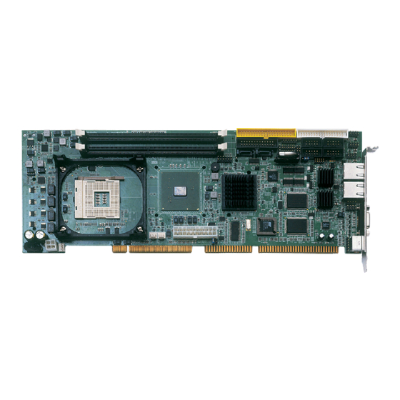
Page 13: Board Layout
Board Layout Top Side Solder Side Jumper List Jumper Default Setting Setting Page CF Use Master/Slave Select: Slave Open Panel Voltage Select: +3.3V Short 1-2 COM 4 Use RS-232 or RS-422/485 Select: Open RS-232 Open FSB Frequency Select: 533MHz Short CN11 Clear CMOS: Normal Operation Short 2-3... -
Page 14: Connector List
Connector List Connector Definition Page CN1/CN2 DDRII Socket System Front Panel Control IDE Connector Parallel Port CN6/CN7 Serial ATA Connector CN8/CN9 LVDS Panel Connector CN10 Floppy Connector CN12 COM 4 Connector (5x2 header) CN13 COM 3 Connector (5x2 header) CN14 COM 2 Connector (5x2 header) CN15 COM 1 Connector (5x2 header) -
Page 15: Configuring The Cpu
Configuring the CPU The 3308270 provides with Intel® Pentium® 4 processor 2.8~3.4GHz. User can select Front Side Bus by JP8/JP9. JP8/JP9: FSB Frequency Select Settings Option 533MHz (default) Open Short 800MHz Short Open System Memory The 3308270 provides two DDRII sockets at locations CN1/CN2. The maximum capacity of the onboard memory is 2GB. - Page 16 CN8/CN9: LVDS Interface Connector PIN Description PIN Description Y0-/Z0- Y0+/Z0+ Y1-/Z1- Y1+/Z1+ Y2-/Z2- Y2+/Z2+ CLK- CLK+ Y3-/Z3- Y3+/Z3+ NOTE: LVDS cable should be produced very carefully. Y0- & Y0+ have to be fabricated in twister pair (Y1- & Y1+, Y2- & Y2+ and so on) otherwise the signal won’t be stable.
-
Page 17: Pci E-Ide Drive Connector
PCI E-IDE Drive Connector CN4 is a standard 40-pin 2.54-pitch connector daisy-chain driver connector serves the PCI E-IDE drive provisions onboard the 3308270. A maximum of two ATA/33/66/100 IDE drives can be connected to the 3308270 via CN4. CN4: IDE Connector Description Description IDERST... -
Page 18: Serial Ata Connector
Serial ATA Connector You can connect the Serial ATA device that provides you high speeds transfer rates (150MB/sec.). If you wish to use RAID function, please note that these two serial ATA connectors just support RAID0 and only compatible with WINXP. CN6/CN7: Serial ATA Connector Description SATATXP... -
Page 19: Floppy Disk Drive Connector
3.10 Floppy Disk Drive Connector The 3308270 uses a standard 34-pin header connector, CN10, for floppy disk drive connection. A total of two FDD drives may be connected to CN10 at any given time. CN10: Floppy Connector Description Description -RWC INDEX# MOA- DSB-... -
Page 20: Parallel Connector
3.11 Parallel Connector CN5 is a standard 26-pin flat cable connector deigned to accommodate parallel port connection on the 3308270. CN5: Parallel Connector Description Description Strobe Auto Form Feed DATA 0 ERROR# DATA 1 Initialize DATA 2 Printer Select LN# DATA 3 DATA 4 DATA 5... - Page 21 JP5: RS-422/485 Connector (3x2 Header) PIN Description PIN Description NOTE: The terminal resistance of RX & TX is set at 180 Ω JP6: COM 4 use RS-232 or RS-422/485 Select Options Settings RS-232 (default) Open RS-485 by Auto (*1) Short 1-2, 3-4, 5-7, 8-10 RS-485 by –RTS (*-1) Short 1-2, 3-4, 7-9, 8-10 RS-422/485 Full Duplex (*2)
-
Page 22: Ethernet Connector
3.13 Ethernet Connector The 3308270 provides two external RJ-45 interface connectors. Please refer to the following for its pin information. CN16/CN17: RJ-45 Connector PIN Description R/C GND R/C GND R/C GND R/C GND JP7: Wake On LAN Description Wake On LAN 3.14 USB Connector The 3308270 provides three 8-pin connectors, at location CN18/CN22/ CN23, for six USB2.0 ports. -
Page 23: Cmos Data Clear
3.15 CMOS Data Clear The 3308270 has a Clear CMOS jumper on CN11. CN11: Clear CMOS Options Settings Normal Operation (default) Short 2-3 Clear CMOS Short 1-2 IMPORTANT: Before you turn on the power of your system, please set CN11 to Open for normal operation. 3.16 Power and Fan Connectors 3308270 provides one 20-pin ATX power in at PW2, and one 4-pin +12V power in at PW1. -
Page 24: Keyboard/Mouse Connectors
R/C GND R/C GND R/C GND JP7: Wake On LAN Description Wake On LAN 3.14 USB Connector The 330827 provides three 8-pin connectors, at location CN18/CN22/ CN23, for six USB2.0 ports. CN18/CN22/CN23: Internal USB2.0 Connector Description Description USBD0-/USBD2-/USBD4- USBD1-/USBD3-/USBD5- USBD0+/USBD2+/USBD4+... -
Page 25: System Front Panel Control
3.18 System Front Panel Control The 3308270 has front panel control at location CN3 that indicates the power-on status. CN3: System Front Panel Control PIN Description Description Speaker HDD LED PWR Button Reset Switch PWR LED Connector CN3 Orientation HDD LED Speaker Button Reset... -
Page 26: Watchdog Timer
3.19 Watchdog Timer Once the Enable cycle is active a Refresh cycle is requested before the time-out period. This restarts counting of the WDT period. When the time counting goes over the period preset of WDT, it will assume that the program operation is abnormal. -
Page 27: Audio Connectors
dx,port ; set CRF5 al,0f5H dx,al dx,datao ; set CRF5 to secend al,00H dx,al dx,port ; set CRF6 time al,0f6H dx,al dx,datao ; set CRF6 time to 5 s' al,05H dx,al print print copyright print ah,4ch ;go back to dos .stack begin endp... -
Page 28: Compactflash Connector
3.21 CompactFlash Connector The 3308270 also offers a Type I/II CompactFlash connector which is IDE interface located at the solder side of the board. The designated CN26 connector, once soldered with an adapter, can hold CompactFlash cards of various sizes. Please turn off the power before inserting the CF card. - Page 29 Inserting a CompactFlash card into the adapter is not a difficult task. The socket and card are both keyed and there is only one direction for the card to be completely inserted. Refer to the diagram on the following page for the traditional way of inserting the card. JP2: CF Use Master/Slave Select Options Setting...
- Page 30 We will do our best to support your products, projects and business. Address: Global American, Inc. 17 Hampshire Drive Hudson, NH 03051 Telephone: Toll Free U.S. Only (800) 833-8999 (603) 886-3900 FAX: (603) 886-4545 Website: http://www.globalamericaninc.com Support: Technical Support at Global American...
Need help?
Do you have a question about the 330827 and is the answer not in the manual?
Questions and answers