
Related Manuals for SIGNALCORE SC5309A


Summary of Contents for SIGNALCORE SC5309A
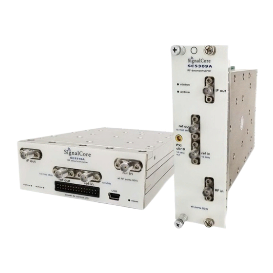
- Page 1 Hardware Manual SC5309A & SC5310A 2.5 GHz RF Downconverter www.signalcore.com © 2018 SignalCore, Inc. All Rights Reserved...
-
Page 2: Table Of Contents
Copyright & Trademarks ........................4 International Materials Declarations ....................5 CE European Union EMC & Safety Compliance Declaration ............. 5 Warnings Regarding Use of SignalCore Products ................6 Physical Description ..........................7 Unpacking ............................7 Setting Up the Device ........................7 Front Interface Indicators and Connectors .................. - Page 3 Device Information Parameters and Format ............... 37 Communication Interfaces ........................1 Communication Data Format ......................1 USB Interface ............................ 1 Control Transfer ........................1 Bulk Transfer ......................... 1 SPI Interface ............................. 2 Rev 2.0 | SC5309A & SC5310A Hardware Manual SignalCore, Inc.
- Page 4 General Information Writing the SPI Bus ........................ 3 Reading the SPI Bus ....................... 3 RS232 Interface ..........................4 Writing to the Device Via RS232 .................... 4 Reading from the Device Via RS232 ..................5 PXI Express ............................5 Setting Up the PCI to Serial Bridge ..................5 Writing to the Device......................
-
Page 5: General Information
SignalCore reserves the right to make changes to subsequent editions of this document without prior notice to possessors of this edition. Please contact SignalCore if errors are suspected. In no event shall SignalCore be liable for any damages arising out of or related to this document or the information contained in it. -
Page 6: International Materials Declarations
General Information products. Use of SignalCore products is restricted to applications that do not infringe on the intellectual property rights of others. “SignalCore”, “signalcore.com”, and the phrase “preserving signal integrity” are registered trademarks of SignalCore, Incorporated. Other product and company names mentioned herein are trademarks or trade names of their respective companies. -
Page 7: Warnings Regarding Use Of Signalcore Products
BECAUSE EACH END-USER SYSTEM IS CUSTOMIZED AND DIFFERS FROM SIGNALCORE'S TESTING PLATFORMS, AND BECAUSE A USER OR APPLICATION DESIGNER MAY USE SIGNALCORE PRODUCTS IN COMBINATION WITH OTHER PRODUCTS IN A MANNER NOT EVALUATED OR CONTEMPLATED BY SIGNALCORE, THE USER OR... -
Page 8: Physical Description
As each device’s integrated system configuration is unique, detailed cooling options cannot be provided. A cooling plan is sufficient when the SC5309A and SC5310A on-board temperature sensors indicate a rise of no more than 20°C above ambient temperature under normal operating conditions. -
Page 9: Front Interface Indicators And Connectors
SC5309A & SC5310A Hardware Manual Front Interface Indicators and Connectors The SC5309A is a PXIe-based RF downconverter with all user I/O located on the front face of the module. Rev 2.0 | SC5309A & SC5310A Hardware Manual SignalCore, Inc. -
Page 10: Signal Connections
Physical Description The SC5310A is a serial controlled core module with all user connections on the front face of the module. Signal Connections All signal connections (ports) on the device are female SMA-type. Exercise caution when fastening cables to the signal connections. Over-tightening any connection can cause permanent damage to the device. -
Page 11: Device Led Indicators
51110-3051 or ribbon type 87568-3093 from Molex. The pin definitions of this I/O connector are listed in Table 3. Pinouts are different for different SignalCore products with the same connector type. Please ensure that mating connectors and cables are wired correctly before connection. -
Page 12: Mini-Usb Connection
Physical Description 2,4,6,8,10,12,16,20,24,28 GND 9,11,13,14,15 Reserved, Do Not Connect 17,18 Reserved, pull high to 3.3V or DNC , System reset, logic 0 to reset device Reset 21 Device Active, accessed 22 PLL status 23 RS232 Baud Rate / SPI Mode Select 25 CS Device select for SPI 26 SPI Clock 27 TX/MOSI. -
Page 13: Reset Button (Pin Hole)
All user settings will be lost. System reset capability can also be accessed through the communication header connector. Rev 2.0 | SC5309A & SC5310A Hardware Manual SignalCore, Inc. -
Page 14: Functional Description
Functional Description 3 Functional Description Overview The SC5310A uses USB as its primary interface with an optional SPI or RS232 interface. The SC5309A is a PXIe version of the product. The downconverter assembly consists of three module parts: • The Signal Conversion Module contains the mixers, filters, signal amplifiers, and attenuators. This module is referred to as the “signal chain”. -
Page 15: The Signal Chain
IF3 Freq = ~10-100 MHz BW= Option option for a From LO Module bandpass 420 MHz – 220 MHz – Figure 4. Block diagram of the signal conversion module of the downconverter assembly Rev 2.0 | SC5309A & SC5310A Hardware Manual SignalCore, Inc. -
Page 16: The Input Path Switch
Functional Description The Input Path Switch Immediately following the capacitor is an RF switch to selectively direct the RF signal down two paths: 1. The default is the conversion path where the RF signal is converted to a final IF. 2. - Page 17 RF and IF1 sections to achieve: 1. Superior image rejection without the use of multiple RF bandpass filters. 2. Great RF suppression and isolation in the IF2 passband without multiple IF and LO frequency bands. Rev 2.0 | SC5309A & SC5310A Hardware Manual SignalCore, Inc.
-
Page 18: The Second Mixer And If2 Path
Functional Description The disadvantage of this approach is the requirement of high IF1 and LO1 frequencies which places demanding phase noise requirements on the LO1 synthesizer. The Second Mixer and IF2 Path The second IF (IF2) is typically centered at 305 MHz and has settable range with 5 MHz steps. The relationship between LO2, IF1, and IF2 is: ����2 = ����1 −... - Page 19 -160 dBm/Hz. The flexible use of these attenuators allows the downconverter to achieve better than 190 dB of measurement dynamic range. Rev 2.0 | SC5309A & SC5310A Hardware Manual SignalCore, Inc.
-
Page 20: The Lo Module
Functional Description The LO Module The local oscillator (LO) module contains three local oscillators, the reference clocks, and the calibration EEPROM as shown in Figure 5. LO Section To Signalchain Module ENABLE CAL EEPROM REF DETECT 100M PLL Reference Section TCXO PLL Programmable component... -
Page 21: The First Local Oscillator (Lo1)
LO3 is set to IF2 - 100 MHz in the inverted case, the IF3 low-pass filters may not sufficiently provide the suppression needed to keep the leakage to an acceptable level at the IF output port. In this case, an external low-pass filter may be needed. Rev 2.0 | SC5309A & SC5310A Hardware Manual SignalCore, Inc. -
Page 22: The Interface Module
Functional Description The Interface Module Figure 6 shows the power and control interface block for both the SC5309A and SC5310A. All supply rails are produced on board; their voltages are regulated and actively filtered to keep noise to a minimum. Thus, these downconverters are tolerant to “dirty” external power supplies. -
Page 23: Hardware Registers
[23:16] Set to zeros [23:16] Bypass Ext. IF2 Bypass [7:0] fil#2 If3 fil#1 select filter select convert SIGNAL_PATH 0x14 select select conv [15:8] Set to zeros [15:10] Rf amp invert Rev 2.0 | SC5309A & SC5310A Hardware Manual SignalCore, Inc. -
Page 24: Register 0X01 Initialize
Hardware Registers Serial Register Name Reg Add Bit 7 Bit 6 Bit 5 Bit 4 Bit 3 Bit 2 Bit 1 Bit 0 Range [23:16] Set to zeros [23:16] Auto Load Auto [7:0] Set to zeros [7:5] Linear mode ctrl params Enable [15:8]... -
Page 25: Register 0X02 System_Active
[7:0] Read back byte Read 1 byte back is required for PXIe and RS232 Register 0x11 IF_FREQUENCY This register sets the final IF value. Bytes written 8 Bytes read 1 Rev 2.0 | SC5309A & SC5310A Hardware Manual SignalCore, Inc. -
Page 26: Register 0X12 Rf_Amp
Hardware Registers Bits Type Name Width Description Frequency word in milli-Hz (mHz); mHz used for [47:0] Frequency word future compatibility [55:48] Used Set to zeros [7:0] Read back byte Read 1 byte back is required for PXIe and RS232 Register 0x12 RF_AMP This register enables and disables the RF amplifier. -
Page 27: Register 0X14 Signal_Path
RF frequency, as computed from its input parameters such as RF input level, mixer level, and IF out level. Bytes written 6 Bytes read 1 Rev 2.0 | SC5309A & SC5310A Hardware Manual SignalCore, Inc. - Page 28 Hardware Registers Bits Type Name Width Description 0 = Attenuator and RF amplifier states are not manipulated when RF values are changed autoGainEnable 1 = Computes and applies new sets of attenuator and amplifier states to the device as frequency is changed 0 = Not to load new input parameter such as RF level, etc.
- Page 29 [7:0] Read back byte Read 1 byte back is required for PXIe and RS232 Register 0x18 REFERENCE_CLOCK This register configures the reference clock behavior. Bytes written 2 Bytes read 1 Rev 2.0 | SC5309A & SC5310A Hardware Manual SignalCore, Inc.
-
Page 30: Register 0X19 Reference_Dac
1 = Enables frequency locking to external 10 MHz reference source RefOutEnable Reference out port enabled 0 = 10 MHz output Clk10Enable 1 = 100 MHz output Only on SC5309A to enable export of the 10 MHz PXI10Enable backplane clock [7:2] Unused Set to zeros [7:0]... -
Page 31: Register 0X1B Synth_Mode (2 Bytes)
This register will start the YIG synthesizer calibration. Note that although the calibration procedure takes about 6-8 seconds to complete, the register returns a byte almost immediately. Bytes written 2 Bytes read 1 Bits Type Name Width Description [7:0] Unused Set to zeros Rev 2.0 | SC5309A & SC5310A Hardware Manual SignalCore, Inc. -
Page 32: Register 0X1D User_Eeprom_Write
Hardware Registers Bits Type Name Width Description [7:0] Read back byte Read 1 byte back is required for PXIe and RS232 Register 0x1D USER_EEPROM_WRITE This register writes a byte to the onboard EEPROM. Bytes written 4 Bytes read 1 Bits Type Name Width Description... -
Page 33: Register 0X20 Get_Device_Param
Returned Data (See Device Parameter Data section [63:0] Read back bytes for more info) Register 0x21 GET_TEMPERATURE Write to this register to query the device temperature. Bytes written 2 Bytes read 8 Rev 2.0 | SC5309A & SC5310A Hardware Manual SignalCore, Inc. -
Page 34: Register 0X22 Get_Device_Status
Hardware Registers Bits Type Name Width Description [7:0] Unused Set to zeros These 32 bits of data need to be type casted back to float. i.e. var_float = *(float*)&var_u32 where [31:0] Temperature Data var_u32 is some unsigned integer that holds the 32 bits of read data. -
Page 35: Register 0X23 Get_Device_Info
Ignore [63:0] Data Information data (see Device Info data) Register 0x24 CAL_EEPROM_READ Write to this register to query 8 bytes of data from the user EEPROM at the starting address. Rev 2.0 | SC5309A & SC5310A Hardware Manual SignalCore, Inc. - Page 36 Hardware Registers Bytes written 4 Bytes read 8 Bits Type Name Width Description [15:0] Address Starting EEPROM address [23:16] Unused Zeros [63:0] Data 8 bytes of data, LSB is the byte at the start address Register 0x25 USER_EEPROM_READ Write to this register to query 8 bytes of data from the user EEPROM at the starting address. Bytes written 4 Bytes read 8 Bits Type...
-
Page 37: Device Parameters Data And Format
The first order computed gain (device approx.) of the device is returned in bytes 3 and 4. Data bits [14:0] represent the absolute value in 1/100 of a dB, while bit [15] is the sign bit. Rev 2.0 | SC5309A & SC5310A Hardware Manual... -
Page 38: Device Information Parameters And Format
Hardware Registers Device Information Parameters and Format Not all the 8 bytes read back contain valid data. The following table shows the valid bytes of data for each of the parameters. Device Param Data Byte 7 Byte 6 Byte 5 Byte 4 Byte 3 Byte 2... - Page 39 Section 2 Communication Interfaces and Calibration © 2018 SignalCore, Inc. All Rights Reserved...
-
Page 40: Communication Interfaces
Communication Interfaces 5 Communication Interfaces The SC5309A has a PXI express interface, while the SC5310A has 2 communication interfaces: 1. USB and SPI 2. USB and RS232 This section will examine the communication aspects of the product, focusing on data transfer to and from the device on each interface. -
Page 41: Spi Interface
The clock rate may be as high as 5.0 MHz (�� �� SPI signals do not have sufficient integrity due to trace issues, the rate should be lowered. Rev 2.0 | SC5309A & SC5310A Hardware Manual SignalCore, Inc. -
Page 42: Writing The Spi Bus
Communication Interfaces Byte N (MSB) DATA 8 Bit Command/ Reg. Address Byte N-1 (LSB) Figure 8. SPI timing. As mentioned above, the SPI architecture limits the byte rate since after every byte transfer the input and output SPI buffers need to be cleared and loaded respectively by the device SPI engine. Data is transferred between the input buffer and internal register buffers. -
Page 43: Rs232 Interface
Failure to complete the register transmission will cause the device to behave erratically or hang. Information for writing to the configuration registers is provided in Table 4. Configuration Registers. Upon the Rev 2.0 | SC5309A & SC5310A Hardware Manual SignalCore, Inc. -
Page 44: Reading From The Device Via Rs232
A simple driver using IO controls should be sufficient to read and write byte data to this block of addresses. Although SignalCore provides the driver and API for these products, information is provided here for users who may need to write drivers for a different operating system or a different driver. -
Page 45: Writing To The Device
8. All 8 bytes must be read to fully clear the transfer buffer; the first byte read is the most significant byte. Rev 2.0 | SC5309A & SC5310A Hardware Manual SignalCore, Inc. -
Page 46: Calibration
Calibration 6 Calibration Calibration EEPROM Map Table 10 represents the EEPROM map of the device calibration values. All values are stored as little- endian 4-byte floating point numbers. Every point is 4-bytes long. Access to the data is possible through the CAL_EEPROM_READ register, which reads 8 bytes starting at the address pointed to by the register input. -
Page 47: Absolute Conversion Gain
Let us call this value ����_����������1. 2. The IF3 Atten#1 attenuation value is read directly from memory: the 15 index of the attenuator array ATTEN3#1[15]. Let us call this correct attenuation value ����3_����������1. Rev 2.0 | SC5309A & SC5310A Hardware Manual SignalCore, Inc. - Page 48 Calibration 3. The IF response can also be read directly from memory, the 3 index (15 MHz/5 MHz) of the IF response array. Let us call this the ����3_����������������. 4. The IF2 filter gain is read directly from memory, which we shall call ����2_������������. 5.
-
Page 49: Revision Table
Revision Date Description 8/10/18 Initial Release 2/26/19 Added feature to signal path register 16. Changed figure 6 to reflect latest conversion path implementation. 4/14/20 Updated tunable IF3 range. 8/13/20 Updated formatting. Rev 2.0 | SC5309A & SC5310A Hardware Manual SignalCore, Inc.
Need help?
Do you have a question about the SC5309A and is the answer not in the manual?
Questions and answers