Table of Contents

Related Manuals for Wiznet WizFi630S


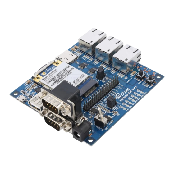
Summary of Contents for Wiznet WizFi630S
- Page 1 WizFi630S Guide WizFi630S Hardware Design Guide (Version 1.0.0) © 2019 WIZnet Co., Ltd. All Rights Reserved. For more information, please visit our website at http://www.wiznet.io/ © Copyright 2019 WIZnet Co., Ltd. All rights reserved.
- Page 2 WizFi630S Guide Document Revision History Date Revision Changes 2019-11-14 Release © Copyright 2019 WIZnet Co., Ltd. All rights reserved.
-
Page 3: Table Of Contents
3. Pin Description ....................... 5 Pin map ......................5 Pin layout......................8 4. Recommended Circuit Diagram................8 Basic schematic Design of the WizFi630S ..........8 USB Host Schematic Design ............... 9 LED Schematic Design ................10 Ethernet Schematic Design ............... 10 Switch Schematic Design ................ - Page 4 WIZnet assumes no responsibilities or liabilities for the use of any of its products, conveys no license or title under any patent, copyright or mask work rights to these products, and makes no representations or warranties that these products are free from patent, copyright or mask work infringement, unless otherwise specified.
-
Page 5: Introduction
This document has been prepared to better help the design-in process of WizFi630S. Please utilize our forum and website for in depth technical support. We greatly welcome and value your feedback and thank you for your interest in WizFi630S. WIZnetForum... - Page 6 10/100 PHY Port #4 RXN TXOP4 GPIO#29 10/100 PHY Port #4 TXP LINK0_LED GPIO#43 LAN port 0 Link LED LINK4_LED GPIO#39 LAN port 4 Link LED LINK3_LED GPIO#40 LAN port 3 Link LED © Copyright 2019 WIZnet Co., Ltd. All rights reserved.
- Page 7 GPIO#0 General Purpose Output LED I/O, IPD LINK1 GPIO#42 WPS LED I2S_DO GPIO#1 GPIO I/O, IPD I2C_SCLK GPIO#4 General Purpose Input Switch SW1-2 I/O, IPD I2C_SD GPIO#5 RUN LED 3.3V 3.3V © Copyright 2019 WIZnet Co., Ltd. All rights reserved.
-
Page 8: Pin Layout
When designing the schematic, the USB HOST line (PADP & PADM) should be paired with the Ethernet line P & M (ex: TXOP0, TXOM0). C37 must be close to the 3.3V and connecting C38 to the Mini PCI Express port will decrease noise. © Copyright 2019 WIZnet Co., Ltd. All rights reserved. -
Page 9: Usb Host Schematic Design
WizFi630S Guide 4.2 USB Host Schematic Design We recommend pairing the USB HOST P and N line, and also place the diode as shown below for ESD protection © Copyright 2019 WIZnet Co., Ltd. All rights reserved. -
Page 10: Led Schematic Design
We also recommend paring the P and N line for Ethernet schematic, and do not place R, L, C, other sign lines below the RJ-45 schematic (especially not below the pair line). The Center-Tap of WizFi630S connects to GND whereas the Center-Tap of WizFi630A operates in 1.8V ~ 3.3V. -
Page 11: Switch Schematic Design
4.5 Switch Schematic Design 4.6 UART0 Micro USB Schematic Design Micro USB P should be paired with N line, and we recommend placing the diode as shown below for ESD protection. © Copyright 2019 WIZnet Co., Ltd. All rights reserved. -
Page 12: Power Supply
WizFi630S Guide 5. Power Supply Power supply is one of the critical parts in the design stage that will affect the performance so please refer to the guidelines below. © Copyright 2019 WIZnet Co., Ltd. All rights reserved. -
Page 13: Power Supply Requirements
Current Rating Caution You must not exceed the voltage rating of DC 3.3V, otherwise WizFi630S will not operate as designed and could cause damage to the device. Also, please design with at least 1.5 or 2 times more current rating (1.5A) ~ (2A) for similar reasons specified ahead. -
Page 14: Dimensions
WizFi630S Guide 6.1 Dimensions Hole HOLE HOLE Length Width Height Width Height Φ Thickness Dimensions (mm) 24.2 Tolerance +/- 0.1mm © Copyright 2019 WIZnet Co., Ltd. All rights reserved.
Need help?
Do you have a question about the WizFi630S and is the answer not in the manual?
Questions and answers