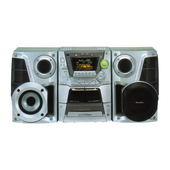
Panasonic SA-AK52 Service Manual
Hide thumbs
Also See for SA-AK52:
- Operating instructions manual (32 pages) ,
- Service manual (80 pages)
Table of Contents
Advertisement
Quick Links
Specifications
AMPLIFIER SECTION
PMPO
RMS power output
THD 10%, both channels driven
80 Hz, both channel driven
(Low channel)
1 kHz, both channel driven
(High channel)
Total Bi-Amp power
Input sensitivity
AUX
MIC
Input Impedance
AUX
MIC
FM TUNER SECTION
Frequency range
Sensitivity
S/N 26 dB
Antenna terminal(s)
AM TUNER SECTION
Frequency range
MW
2300 W
100 W per channel (6 Ω)
40 W per channel (6 Ω)
140 W per channel
250 mV
0.7 mV
13 kΩ
680 Ω
87.5 - 108 MHz (50 kHz steps)
2.5 µV (IHF)
2.2 µV
75 Ω (unbalanced)
522 - 1629 kHz (9 kHz steps)
520 - 1630 kHz (10 kHz steps)
CD Stereo System
Colour
(S)... Silver Type
Area
(GC)...Asia, Latin America, Africa and Middle Near East
TAPE SECTION :
AR2 MECHANISM SERIES
CD SECTION :
RAE0152Z-3 TRAVERSE DECK SERIES
SW
Sensitivity
MW
S/N 20 dB (at 999 kHz)
SW
S/N 20 dB (at 5.3 MHz)
Track system
Heads
Record/playback
Erasure
Motor
Recording system
Erasing system
Tape speed
Frequency response (+3 dB, -6 dB at DECK OUT)
NORMAL (TYPE I)
HIGH (TYPE II)
S/N
Wow and flutter
Fast forward and rewind time
© 2001 Matsushita Electronics (S) Pte Ltd. All rights
reserved. Unauthorized copying and distribution is a
violation of law.
ORDER NO. MD0101010C3
3.200 - 7.350 MHz (0.005 MHz
steps)
9.400 - 21.750 MHz (0.005 MHz
steps)
560 µV/m
35.5 µV/m
4 track, 2 channel
Solid permalloy head
Double gap ferrite head
DC servo motor
AC bias 100 kHz
AC erase 100 kHz
4.8 cm/s
35 Hz - 14 kHz
35 Hz - 14 kHz
50 dB (A weighted)
0.18% (WRMS)
Approx. 120 seconds with
Advertisement
Table of Contents
Troubleshooting

Related Manuals for Panasonic SA-AK52


Summary of Contents for Panasonic SA-AK52
- Page 1 ORDER NO. MD0101010C3 CD Stereo System SA-AK52 Colour (S)... Silver Type Area (GC)...Asia, Latin America, Africa and Middle Near East TAPE SECTION : AR2 MECHANISM SERIES CD SECTION : RAE0152Z-3 TRAVERSE DECK SERIES Specifications AMPLIFIER SECTION 3.200 - 7.350 MHz (0.005 MHz...
- Page 2 Mass 9.0 kg Beam source/wave length Semiconductor laser/780 nm SYSTEM Number of channels Stereo SC-AK52(GC) Music Center: SA-AK52(GC) Frequency response 20 Hz - 20 kHz (+1, -2 dB) Speaker: SB-AK52(GC) Wow and flutter Below measurable limit Notes: Digital filter 8 fs 1.
- Page 3 SA-AK52 1 Before Use Be sure to disconnect the mains cord before adjusting the voltage selector. Use a minus(-) screwdriver to set the voltage selector (on the rear panel) to the voltage setting for the area in which the unit will be used.
- Page 4 SA-AK52 5 Handling Precautions For Traverse Deck The laser diode in the traverse deck (optical pickup) may break down due to potential difference caused by static electricity of clothes or human body. So, be careful of electrostatic breakdown during repair of the traverse deck (optical pickup).
- Page 5 SA-AK52 6 Precaution of Laser Diode Caution : This product utilizes a laser diode with the unit turned "ON", invisible laser radiation is emitted from the pick up lens. Wavelength : 780 nm Maximum output radiation power from pick up : 100 µW/VDE Laser radiation from pick up unit is safety level, but be sure the followings: 1.
- Page 6 SA-AK52 7 Operation Procedures...
- Page 7 SA-AK52...
- Page 8 SA-AK52 8 Operation Checks and Main Component Replacement Procedures “ATTENTION SERVICER” Some chassis components may have sharp edges. Be careful when disassembling and servicing. 1. This section describes procedures for checking the operation of the major printed circuit boards and replacing the main components.
- Page 9 SA-AK52 8.1. Disassembly and assembly main unit Step 1 Remove 3 screws each side and 5 screws at rear panel. Step 2 Remove the Top Cabinet Step 3 Remove T-bracket. Step 4 Remove 2 screws each side of the inner chassis and a screw at the rear panel.
- Page 10 SA-AK52 Step 4 : Remove the CD lid in the direction of the arrow. Step 5 : Release the two catches shown above to remove the Step 1 : Use a hexagonal wrench and turn clockwise to release front cabinet from the CD Traverse Unit.
- Page 11 SA-AK52 Step 7 Remove 2 screws from bottom and 2 screw beside Step 8 To release inner bracket, remove 4 screws. inner bracket to push forward to release the front panel. 8.1.1. Checking for Panel, Main and Deck P.C.B. Step 1 Remove 2 screws each side.
- Page 12 SA-AK52 8.1.2. Checking for Power P.C.B. 8.1.3. For Live Troubleshooting Procedure Step 6 : Reconnect all connectors. Step 7 : Use extension 14pin FFC wire for CN309. Step 8 : Supply power for troubleshooting.
- Page 13 SA-AK52 8.2. Main Component Replacement Procedures 8.2.1. Replacement of the Traverse Deck Step 1 Follow the procedures in ‘Disassembly of the Traverse Unit’ ( Step 1 - Step 4 ). Step 5 Remove the flexible cable CN701. Step 3 Desolder the 4 legs of the 2 motors and pull out the •...
- Page 14 SA-AK52 Note: Before installing the CD servo P.C.B., move the optical pickup towards the outer edge from the marking (black triangle). [Otherwise, the reset detect switch (S701) mounted on the CD servo P.C.B. may be damaged.] 8.2.2. Replacement of the Power Amplifier IC Step 1 Follow the procedures in ‘Checking Procedure for each...
- Page 15 SA-AK52 8.3. Disassembly and assembly of the Traverse Unit Step 1 Push the lever from position A to B. Step 2 Pull the stopper (black) in the direction of arrow 1 and push the lever in the direction of arrow 2.
- Page 16 SA-AK52 8.4. Disassembly and assembly of the Disc Tray (clockwise), and then open the disc tray fully. Step 2 With lifting the claw in the direction of arrow 1, draw the Step 6 Upset the CD changer unit again. clamp SW P.C.B. in the direction of arrow 2.
- Page 17 SA-AK52 Step 1 Slide the drive rack fully in the direction of the arrow. Step 4 Holding the disc tray manually, rotate the pulley gear in the direction of arrow. Step 5 Rotate the gear 5 or 6 times manually, and then push the disc tray.
- Page 18 SA-AK52 9 Self-Diagnostic Function 9.1. Self-diagnostic display This unit is equipped with a self-diagnostic display function which, if a problem occurs, will display an error code corresponding to the problem. Use this function when performing maintenance on the unit. 9.2.
- Page 19 SA-AK52 7. Press “ /TUNE MODE” to indicate Error Code. • If several problem exist, error code will change each time when “ /TUNE MODE” is pressed. (e.g. F15 → F26 → F16 ..etc). 9.5. To clear all Error code 1.
- Page 20 SA-AK52 11 CD Test Mode Function This CD test mode is provided to check CD unit without 11.2. CD Automatically Adjustment connecting to changer loading mechanism. This mode shall result indication operate CD PLAY with CD unit being connected only and CD Automatic Alignment result is shown on FL display.
- Page 21 SA-AK52 12.1.3. Bias and Erase Voltage Check 1. Set the unit “AUX” position. 2. Insert the Normal blank tape (QZZCRA) into DECK 2 and the unit to “REC” mode (use “ REC/STOP” key). 3. Measure and make sure that the output is within the standard value.
- Page 22 SA-AK52 12.2.2. AM-RF Alignment SIGNAL GENERATOR OR SWEEP RADIO DIAL SETTING INDICATOR ADJUSTMENT REMARKS GENERATOR (ELECTRONIC (Shown in Fig.3) VOLTMETER CONNECTIONS FREQUENCY OSCILLOSCOPE) Fashion a loop of 522 kHz Tuning capacitor fully closed Headphones Jack (32Ω) Z152 (GC), Adjust for maximum output.
- Page 23 SA-AK52 12.3. Alignment Points Cassette Deck section Tuner section...
- Page 24 SA-AK52 13 Illustration of IC’s, Transistors and Diodes M38B79MFA053(100P) RSN309W44B TA7291P M5218AP BU2090AF-E2 (16P) BH3874AKS2 (64P) 93LC46B LA1833NMNTLM (24P) MN662790RSC (80P) LC72131MDTRM (20P) AN7348STA-E1 (24P) BA4558FE2 (8P) AN8885SBE1 (28P) TC4052BFNELM (16P) 2SC2058SPTA 0N2180RLC1 AN8739SBE2 KIA4558FEL BA7755A KTC2026 2SA1309ARTA KTA1046 KBP152G4R5...
- Page 25 SA-AK52 14 Terminal Function of ICs 14.1. IC701 (AN8885SBE1) Servo Amplifier Pin No. Mark Function Pin No. Mark Function Tracking signal input 1 /RFDET NRFDET output (“L” : detection) Tracking signal input 2 PDOWN Power-down input Power supply OFTR OFTR output Focus signal input terminal 1 N.C.
- Page 26 SA-AK52 Mark Function Mark Function EFM signal output CLVS Spindle servo phase synchronizing signal output PLL extraction clock output ("H" : CLV, "L" : rough servo) (fPCK = 4.321 MHz during normal playback) Sub-code checked output (“H” :OK, “L” :NG) VCOF2 VCO Loop filter for 33.8688...
- Page 27 SA-AK52 Pin No. Mark Function CNVSS Flash mode terminal (connect to ground) /RESET RESET input XCOUT 32.768 kHz sub clock XCIN 32.768 kHz sub clock Ground (0V) 4.19 MHz main clock XOUT 4.19 MHz main clock Power supply (+5V) MBP1...
- Page 28 SA-AK52 15 Block Diagram OPTICAL PICKUP IC701 AN8885SBE1 SERVO AMP SEMICONDUCTOR LASER OFTR TENV DET. Q701 LASER POWER DRIVE OFTR OFTR DET. LDON /RFDET /RFDET DET. PHOTO DETECTOR FEOUT Subtracter VCBA VREF Subtracter VCBA N.C. TRACKING FOCUS COIL COIL TX 6...
- Page 29 SA-AK52 FM ANT CF201 CF202 Z120 Q101 MIXER IF AMP RF AMP BUFFER IC101 LA1833NMNTLM FM/AM IF AMP, DET/AM OSC, MIX/FM MPX (FM) Q152 Q151 SWITCH SWITCH Z151 COIL COIL DECODER RF AMP AM ANT BUFFER PILOT PHASE CANCEL Q158...
- Page 30 SA-AK52 TA7291P MOTOR DRIVE Vs 8 OUT1 OUT2 POWER SUPPLY CONTROL Q604 STATUS SWITCH Q605 SUBQ SWITCH D614 ST/DO Q350 Q606 SWITCH BLKCK (PLUNGER SWITCH SUPPLY) /CDRST Q351 RESTSW SWITCH (PLUNGER SUPPLY) D619 D615 CE/MLD MLD/PLLCE D616 DI/MDATA MDATA/PLLDA D617...
- Page 31 SA-AK52 IC1001 AN7348STA-E1 P.B. EQ /TPS AMP Q1012(Q1013) REC AMP/ALC (DECK 1) IC1003 P.B. HEAD LCH MUTING 24(23) BA4558FE2 1(2) 20(5) BUFFER 22(3) Q1014 (Q1015) (DECK 2) 21(4) Q1024 R/P HEAD LCH BUFFER 17(8) DRIVE 18(7) LOGIC L/H NOR/CrO &...
- Page 32 SA-AK52 FILTER FILTER 23~27 (10) (13) (14) IC302 M5218AP Q400(Q200) (31) BUFFER MUTING OUTL(R) 45(46) INLC(R) Q300 MUTING IC301 SWITCH BH3874AKS2 ASP IC Q309,Q310 51(52) RECL(R) MUTING SWITCH 43(44) INLB(R) 47(48) IC304 INLD(R) JK305 KIA4558FEL D572,D573 DUAL 41(42) CD SIGNAL...
- Page 33 SA-AK52 SIGNAL LINES MAIN SIGNAL LINE CD SIGNAL LINE AM SIGNAL LINE PLAYBACK SIGNAL LINE H_OUT_L(R) FM OSC SIGNAL LINE AM OSC SIGNAL LINE FM & AM SIGNALS LINE RECORDING SIGNAL LINE FM SIGNAL LINE AUX SIGNAL LINE HP_L(R) IC500...
- Page 34 SA-AK52 16 Schematic Diagram (All schematic diagrams may be modified at any time with the S944 3D AI EQ switch development of the new technology) S945 Super sound EQ switch S950 Disc 2 switch Note: S951 Sub woofer switch S952...
- Page 35 SA-AK52 SCHEMATIC DIAGRAM -1 : CD SIGNAL LINE : +B SIGNAL LINE : +B SIGNAL LINE CD SERVO CIRCUIT R701 OPTICAL PICKUP CIRCUIT Q701 C701 2SA1037AKSTX 6.3V33 3.2V C703 LASER POWER DRIVE LASER DIODE 6.3V100 Q701 CN701 2.7V ((2.3V)) 0.9V...
- Page 36 SA-AK52 SCHEMATIC DIAGRAM - 2 : CD SIGNAL LINE : +B SIGNAL LINE : +B SIGNAL LINE R717 C727 50V1 C725 1000P R721 C726 1000P R718 C728 50V1 C731 6.3V220 CN702 Lch OUT C730 C733 C732 A.GND 6.3V220 C754 Rch OUT 470P +3.3V...
- Page 37 SA-AK52 SCHEMATIC DIAGRAM - 3 : AM SIGNAL LINE : FM SIGNAL LINE : +B SIGNAL LINE : FM OSC SIGNAL LINE : AM OSC SIGNAL LINE MAIN/TUNER CIRCUIT Z120 (RAL0029) C103 0.01 2SC2786M R107 2SK544 FM MIXER C104 R106...
- Page 38 SA-AK52 SCHEMATIC DIAGRAM - 4 : AM SIGNAL LINE : FM SIGNAL LINE : +B SIGNAL LINE : FM OSC SIGNAL LINE : AM OSC SIGNAL LINE : FM/AM SIGNAL LINE R104 CF202 R121 C120 16V10 C116 C138 0.033 0.01 13.6V...
- Page 39 SA-AK52 SCHEMATIC DIAGRAM - 5 : +B SIGNAL LINE : MAIN SIGNAL LINE : FM/AM SIGNAL LINE : -B SIGNAL LINE : RECORD SIGNAL LINE : CD SIGNAL LINE PANEL CIRCUIT (CP605) ON SCHEMATIC DIAGRAM-9 MAIN CIRCUIT CN303 20 19 18 17 16 15 14 13 12 11 10...
- Page 40 SA-AK52 SCHEMATIC DIAGRAM - 6 : -B SIGNAL LINE : MAIN SIGNAL LINE : +B SIGNAL LINE PANEL CIRCUIT (CP607) ON SCHEMATIC DIAGRAM-9 CN302 24 23 22 21 20 19 18 17 16 15 14 13 12 11 10 C375...
- Page 41 SA-AK52 SCHEMATIC DIAGRAM - 7 : +B SIGNAL LINE : -B SIGNAL LINE : MAIN SIGNAL LINE (-29.86V)<-29.85V> (-44.1V)<-43.8V> -29.89V((-29.84V)) -43.9V((-42.9V)) RL1N4003S-P [-29.94V] [-44.2V] R332 D313 C359 R331 (-30.45V) 0.01 4.7K <-30.48V> Q308 -30.5V C360 ((-30.44V)) 63V100 CN301 [-30.55V] 2SB621ARSTA...
- Page 42 SA-AK52 SCHEMATIC DIAGRAM - 7 : +B SIGNAL LINE : CD SIGNAL LINE : MAIN SIGNAL LINE PANEL CIRCUIT FL600 RSL0310-F C600 35V22 TACT SWITCH (1) CIRCUIT IC602 BU2090AF-E2 Z940 RCD37142TC5 IO EXP 2 REMOTE CONTROL SENSOR <0.45V> <0.13V> C941 (0.13V)
- Page 43 SA-AK52 SCHEMATIC DIAGRAM - 8 DECK CIRCUIT : +B SIGNAL LINE : MAIN SIGNAL LINE (CN1001) ON SCHEMATIC DIAGRAM-10 : -B SIGNAL LINE : CD SIGNAL LINE H600 Q603 2SA933SSTA SWITCH C634 DECK +6V SUPPLY R651 R652 35V22 D613 L605...
- Page 44 SA-AK52 SCHEMATIC DIAGRAM - 9 : +B SIGNAL LINE : PLAYBACK SIGNAL LINE : -B SIGNAL LINE : RECORD SIGNAL LINE DECK CIRCUIT R1055 2.2K R1098 C1038 220P R1017 8.2K CS1001 R1095 100K R1032 R1015 HEAD C1015 C1012 C1034 1000P...
- Page 45 SA-AK52 SCHEMATIC DIAGRAM - 10 : +B SIGNAL LINE : PLAYBACK SIGNAL LINE : -B SIGNAL LINE : RECORD SIGNAL LINE MAIN CIRCUIT (CN304) ON SCHEMATIC DIAGRAM-4 H1001/W1001 10 9 R1072 R1077 R1074 C1057 C1058 C1060 50V3.3 R1069 4700P 6.8K...
- Page 46 SA-AK52 SCHEMATIC DIAGRAM - 12 : +B SIGNAL LINE : -B SIGNAL LINE : MAIN SIGNAL LINE POWER CIRCUIT IC500 IC500 RSN309W44B POWER IC DISP -VCC +VCC -VCC +VCC L IN R IN -CIN +CIN RELAY HMUT +COUT -COUT AC IN...
- Page 47 SA-AK52 SCHEMATIC DIAGRAM -13 AC TRANSFORMER CIRCUIT (9.74V) <9.74V> Q573 (15.04V) <15.04V> 10.04V ((9.60V)) 15.05V ((14.94V)) D570 R570 R571 R572 2SD2144STA [10.23V] [15.02V] Q573 REGULATOR (8.73V) <8.73V> 9.07V ((8.62V)) (5.92V) <5.96V> [9.15V] 5.96V ((5.94V))[5.97V] R581 820K Q570 (9.19V) <9.06V> D581 8.86V ((8.22V))
- Page 48 SA-AK52 17 Printed Circuit Board Note: Circuit board diagrams may be modified at any time with the development of new technology. CD SERVO P.C.B (REPX0192D) (RF) TP20 X701 TJ701 TP23 C717 R714 TP19 TP21 TP29 C716 C721 R709 C744 TP24...
- Page 49 SA-AK52 MAIN / TUNER P.C.B. (REPX0250A) FM LOOP ANTENNA MW ANT SW ANT 75OHMS JK101 R402 R171 C374 C402 L104 C202 R401 C159 J260 R202 C376 Z120 (TUNER PACK) JK305 R156 R168 R165 Q311 Z152 J259 D151 J151 R164 J258...
- Page 50 SA-AK52 PANEL P.C.B. (REPX0231B) S951 D611 S.WOOFER Q601 Q699 R997 R651 J983 D697 J695 R996 D694 R614 D699 D695 R613 R615 J985 J999 D693 D696 D690 R612 R955 R616 J997 R611 J612 J996 L605 J611 J900 J670 J671 R603 J613...
- Page 51 SA-AK52 HEADPHONE P.C.B. (REPX0231B) HEADPHONES H920B/W920 1 2 3 4 5 6 D605 J600 J955 J602 FL600 R620 C921 J604 R621 H940A/W940 R920 R622 C920 S956 1 2 3 4 5 6 7 8 9 J610 R647 J690 R693 IC602...
- Page 52 SA-AK52 TACT SWITCH (2) P.C.B. TACT SWITCH (1) P.C.B. (REPX0231B) (REPX0231B) VOLUME CP900 R949 R948 R918 R917 R947 R942 R912 R916 R946 R915 R914 J956 C941 C940...
- Page 53 SA-AK52 MECHANISM (DECK1) P.C.B (REPX0108) S953 CR02 CS951 S952 HALF S951 MODE D951 IC951 SOLENOID MECHANISM (DECK2) P.C.B (REPX0108A) S973 CR02 Z971 CS971 1 2 3 4 5 6 7 8 9 S972 S971 HALF MODE S974 S975 D971 IC971 SOLENOID TUNER PACK P.C.B (REP1999B)
- Page 54 SA-AK52 CD LOADING P.C.B (REP2578A-N) 1 2 3 4 5 6 7 8 9 10 2 3 4 CD DETACT P.C.B SPINDLE POSITION P.C.B (REP2578A-N) (REP2578A-N) 1 2 3 4...
- Page 55 SA-AK52 DECK P.C.B. (REPX0198B) J1046 C1062 R1096 J1072 C1059 H1001/W1001 R1092 C1061 R1091 R1095 R1094 R1093 J1062 J1051 W1002 R1062 J1015 J1071 J1028 J1059 J1080 J1016 J1060 J1069 R1064 R1063 R1024 R1020 R1027 J1017 J1075 J1068 J1067 J1052 J1047 J1021...
- Page 56 SA-AK52 POWER P.C.B. (REPX0233B) HIGH-CHANNEL LOW-CHANNEL SPEAKERS SPEAKERS J508 J513 C526 C530 J524 J529 R535 R537 J541 C524 C528 R534 C500 J534 J540 J520 R502 CP501 J547 R516 C505 E500 D508 D503 C508 Q502 R510 R519 R512 C512 Q504 R523...
- Page 57 SA-AK52 AC TRANSFORMER P.C.B. (REPX0251A) CAUTION RISK OF ELECTRIC SHOCK AC VOLTAGE LINE. PLEASE DO NOT TOUCH THIS P.C.B RL502 T501 (POWER TRANSFORMER) D574 R582 Q572 D580 R580 R574 W500 C578 R577 D576 R576 R583 D578 Q570 J578 CN502 R570...
- Page 58 SA-AK52 18 Wiring Connection Diagram H-CHANNEL L-CHANNEL FM ANT AM ANT SPEAKERS SPEAKERS OPTICAL L- R- L+ R+ L- R- L+ R+ SOLDER SIDE JK501 JK500 JK101 TUNER PACK P.C.B CN300 CD LOADING P.C.B Z101 MIC P.C.B SOLDER SIDE CP501...
- Page 59 SA-AK52 19 Troubleshooting Guide...
- Page 60 SA-AK52 20 Parts Location and Replacement Parts List Notes: • Important safety notice: Components identified by mark have special characteristics important for safety. Furthermore, special parts which have purposes of fire-retardent (resistors), high-quality sound (capacitors), low noise (resistors), etc are used.
- Page 61 SA-AK52 20.1. Deck Mechanism (RAA3408) 20.1.1. Deck Mechanism Parts Location...
- Page 62 SA-AK52...
- Page 63 SA-AK52 20.1.2. Deck Mechanism Parts List Ref. No. Part No. Part Name & Description Remarks CASSETTE DECK RED0050 R/P HEAD BLOCK UNIT 101-1 RHE5152ZB SCREW RED0051 P/B HEAD BLOCK UNIT 102-1 RHE5152ZB SCREW RDG0300 REEL BASE GEAR RDG0301 WINDING RELAY GEAR...
- Page 64 SA-AK52 20.2. CD Loading Mechanism (RD-DAC026-S) 20.2.1. CD Loading Mechanism Parts Location...
- Page 65 SA-AK52...
- Page 66 SA-AK52 20.2.2. CD Loading Mechanism Parts List Ref. No. Part No. Part Name & Description Remarks Ref. No. Part No. Part Name & Description Remarks TRAVERSE DECK XTN2+6G SCREW RMX0141 PUSH SPACER RML0517 TIMING LEVER RMQ0749 UPPER SPINDLE RML0516 PLUNGER LEVER...
- Page 67 SA-AK52 20.3. Cabinet 20.3.1. Cabinet Parts Location...
- Page 68 SA-AK52...
- Page 69 SA-AK52...
- Page 70 SA-AK52 20.3.2. Cabinet Parts List Ref. No. Part No. Part Name & Description Remarks Ref. No. Part No. Part Name & Description Remarks CABINET AND CHASSIS RKWX0156A-1 FL FILTER RMBX0016-1 CASS. OPEN SPRING REEX0129 14P FFC RMKX0043 BOTTOM CHASSIS REEX0101-1...
- Page 71 SA-AK52 Ref. No. Part No. Part Name & Description Remarks Ref. No. Part No. Part Name & Description Remarks Q307 KRC111STA TRANSISTOR D316 RL1N4003S-P DIODE Q308 2SB621ARSTA TRANSISTOR D318 UDZSTE177R5B DIODE Q309 KTA1504GRTA TRANSISTOR D319 MA728TX DIODE Q310 KTC3875GRTA TRANSISTOR...
- Page 72 SA-AK52 Ref. No. Part No. Part Name & Description Remarks Ref. No. Part No. Part Name & Description Remarks D1003 1SS355TE17 DIODE CN900 RJT066H12F 12P BTB CONNECTOR D1004 UDZTE173R6B DIODE CN1001 RJS8T7ZA 8P MOLEX VARIABLE RESISTORS CP500 RJT057G12 12P P2 MQ CONNECTOR...
- Page 73 SA-AK52 Ref. No. Part No. Part Name & Description Remarks Ref. No. Part No. Part Name & Description Remarks EYF52BC FUSE HOLDER R104 ERJ3GEYJ102V 1K 1/16W EYF52BC FUSE HOLDER R105 ERJ3GEYJ471V 470 1/16W EYF52BC FUSE HOLDER R106 ERJ3GEYJ474V 470K 1/16W...
- Page 74 SA-AK52 Ref. No. Part No. Part Name & Description Remarks Ref. No. Part No. Part Name & Description Remarks R225 ERJ3GEYJ392V 3.9K 1/16W R401 ERJ3GEYJ272V 2.7K 1/16W R226 ERJ3GEYJ121V 120 1/16W R402 ERJ3GEYJ103V 10K 1/16W R227 ERJ3GEY0R00V 0 1/16W R407 ERJ3GEYJ152V 1.5K 1/16W...
- Page 75 SA-AK52 Ref. No. Part No. Part Name & Description Remarks Ref. No. Part No. Part Name & Description Remarks R583 RSFMB40KT-L FUSE PROTECTOR R676 ERDS2TJ472T 4.7K 1/4W R600 ERDS2TJ472T 4.7K 1/4W R677 ERDS2TJ681T 680 1/4W R601 ERDS2TJ472T 4.7K 1/4W R678...
- Page 76 SA-AK52 Ref. No. Part No. Part Name & Description Remarks Ref. No. Part No. Part Name & Description Remarks R931 ERDS2TJ334T 330K 1/4W R1047 ERJ3GEYJ102V 1K 1/16W R932 ERDS2TJ822T 8.2K 1/4W R1048 ERJ3GEYJ102V 1K 1/16W R933 ERDS2TJ334T 330K 1/4W R1049...
- Page 77 SA-AK52 Ref. No. Part No. Part Name & Description Remarks Ref. No. Part No. Part Name & Description Remarks C107 ECUV1H472KBV 4700P 50V C310 ECUV1C473KBV 0.047 16V C109 ECUV1H102KBV 1000P 50V C311 ECEA1HKAR33B 0.33 50V C110 ECUV1H103KBV 0.01 50V C312 ECEA1HKAR15B 0.15 50V...
- Page 78 SA-AK52 Ref. No. Part No. Part Name & Description Remarks Ref. No. Part No. Part Name & Description Remarks C434 ECEA1HKA4R7B 4.7 50V C629 ECBT1H561KB5 560P 50V C435 ECEA1HKA2R2B 2.2 50V C630 ECBT1H561KB5 560P 50V C436 ECEA1HKA2R2B 2.2 50V C631 ECBT1E103ZF5 0.01 25V...
- Page 79 SA-AK52 Ref. No. Part No. Part Name & Description Remarks Ref. No. Part No. Part Name & Description Remarks C919 ECBT1H101KB5 100P 50V C920 ECBT1E223ZF5 0.022 25V CHIP JUMPER C921 ECBT1E223ZF5 0.022 25V C930 ECBT1E223ZF5 0.022 25V RJ701 ERJ6GEY0R00V 0 1/10W...
- Page 80 SA-AK52 20.5. Packing Materials & Accessories Parts List Ref. No. Part No. Part Name & Description Remarks Ref. No. Part No. Part Name & Description Remarks PACKING MATERIALS N2QAGB000004 REMOTE CONTROLLER A1-1 RKK-HTR0280 R/C BATTERY COVER RPGX0706 PACKING CASE RJA0019-2K...
Need help?
Do you have a question about the SA-AK52 and is the answer not in the manual?
Questions and answers