Sony VPL-FH31 Service Manual
Rm-pj19
Hide thumbs
Also See for VPL-FH31:
- Quick reference manual (148 pages) ,
- Manual (116 pages) ,
- Operating instructions manual (69 pages)

Related Manuals for Sony VPL-FH31


Summary of Contents for Sony VPL-FH31
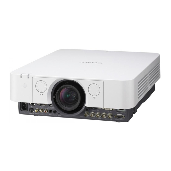
- Page 1 DATA PROJECTOR VPL-FH31 VPL-F401H REMOTE COMMANDER RM-PJ19 SERVICE MANUAL 1st Edition...
- Page 2 WARNUNG VPL-FH31 Beim Einbau des Geräts ist daher im Festkabel ein leicht zugänglicher Unterbrecher einzufügen, oder das Netzkabel muß mit einer in der Nähe For kundene i Norge des Geräts befi...
- Page 3 Batterien nur durch den vom Hersteller empfohlenen Kasser batteriet i henhold til gjeldende avfallsregler. oder einen gleichwertigen Typ ersetzen. Wenn Sie die Batterie entsorgen, müssen Sie die Gesetze der jeweiligen Region und des jeweiligen Landes befolgen. 注意 注意 如果更换的电池不正确,就会有爆炸的危险。 只更换同一类型或制造商推荐的电池型号。 处理电池时,必须遵守相关地区或国家的法律。 1 (P) VPL-FH31/F401H...
-
Page 5: Table Of Contents
Main (Scan Converter)........2-8 (E) 1-3-23. Out-polarizer (R)/(G)/(B) Assembly and 2-6-3. Sub ..............2-9 (E) Out-pre-polarizer (R)/(G)/(B) Assembly ..1-28 (E) 2-6-4. Ext (Network) ..........2-10 (E) 1-3-24. PS Assembly (P/S Converter) ......1-29 (E) 2-6-5. Ext (Network) Reset ........2-10 (E) 1-3-25. Shift ..............1-29 (E) 1 (E) VPL-FH31/F401H... - Page 6 4. Block Diagrams Overall ................4-2 5. Schematic Diagrams C ..................5-2 GB ................. 5-24 H ..................5-26 NF .................. 5-27 QA ................. 5-28 QB ................. 5-33 QC ................. 5-34 U ..................5-35 V ..................5-35 Frame Wiring..............5-36 2 (E) VPL-FH31/F401H...
-
Page 7: Manual Structure
Manual Structure Purpose of this manual This manual is the Service Manual of the Data Projector VPL-FH31/F401H. This manual contains the service overview, adjustments, spare parts, block diagrams, schematic diagrams and board layouts. Related manuals In addition to this Service Manual, the following manuals are provided. -
Page 9: Service Overview
Section 1 Service Overview 1-1. Appearance Figure/Board Locations Appearance Board Locations C board Power supply unit U board (Main) GB board H board NF board QB board QC board Power supply unit (Lamp) QA board V board 1-1 (E) VPL-FH31/F401H... -
Page 10: Tighten Torque
0.80 ?0.12 N.m (8.16 ?1.22 kgf.cm) . Lens fixing screw (with stopper): 0.70 ?0.10 N.m (7.14 ?1.02 kgf.cm) . Screw (with stopper): 0.70 ?0.10 N.m (7.14 ?1.02 kgf.cm) . Connector screw: 0.53 N.m (5.40 kgf.cm) +0.07 +0.71 _0.06 _0.61 1-2 (E) VPL-FH31/F401H... -
Page 11: Disassembly
Remove parts in the order of numbers shown in the figure, in this section. 1-3-1. Lens Cover Assembly 1-3-20. Lens 1-3-1. Lens Cover Assembly 1-3-3. Top Panel Assembly and H Board 1-3-4. GB board 1-3-5. C Board 1-3-18. NF Board 1-3-4. GB board 1-3 (E) VPL-FH31/F401H... - Page 12 1-3-6. Power Supply Unit (Main) 1-3-13. Gear Block 1-3-7. DC Fan (For Power Supply Unit (Main)) 1-3-24. PS Assembly (P/S Converter) 1-3-10. DC Fan (For lamp) and 1-3-11. DC Fan Fuse Connector Assembly (For Power Supply Unit (Lamp)) 1-4 (E) VPL-FH31/F401H...
- Page 13 1-3-15. QB Board and QC Board 1-3-12. Power Supply Unit (Lamp) 1-3-16. DC Fan 1-3-22. Prism Assembly 1-3-21. In-polarizer (R)/(G)/(B) Assembly (Panel R/B and Panel G (For Intake)) 1-3-17. V Board 1-3-23. Out-polarizer (R)/(G)/(B) Assembly 1-3-25. Shift and Out-pre-polarizer (R)/(G)/(B) Assembly 1-5 (E) VPL-FH31/F401H...
-
Page 14: Lens Cover Assembly
Three grooves of the top panel assembly Three convex portions of the lens cover assembly 2 Lens cover assembly 1 Loosen the two screws (M3) (with stoppers). 1-6 (E) VPL-FH31/F401H... -
Page 15: Rear Panel Assembly
5 Rear panel assembly 2 Four hooks Four holes of the top panel assembly 2 Four hooks 5 Rear panel assembly 1 Loosen the three screws (M3) (with stoppers). 4 Sheet (RP) 3 Nylon rivet 1-7 (E) VPL-FH31/F401H... -
Page 16: Top Panel Assembly And H Board
!= Button (H) connector (CN11) on the H board. !- H board !/ Holder (H) 9 Nylon rivet 2 Seven screws (BVTP3 x 12) 1 Two screws (PSW M3 x 70) 1-8 (E) VPL-FH31/F401H... -
Page 17: Board
1-3-4. GB board 5 Four screws (BVTP3 x 12) 1 Harness CN2601 CN2603 CN2602 3 Harness 2 Harness 6 GB board CN2501 4 Harness Rear side of this unit 1-9 (E) VPL-FH31/F401H... -
Page 18: C Board
CN1701 Power supply unit (Lamp) CN303 H board CN202 CN201 NF board CN1601 CN1801 Prism assembly (B) Prism assembly (R) Prism assembly (G) V board CN301 QC board CN106 CN102 CN101 QA board QA board C board 1-10 (E) VPL-FH31/F401H... - Page 19 (IC) facing the shield (CT) side. 9 C board 3 Three harnesses 0 Screw (PSW3 x 8) 8 Two connectors (B to B) 7 Three flexible flat cables !- WU shield (CB) 1-11 (E) VPL-FH31/F401H...
-
Page 20: Power Supply Unit (Main)
1 Open the wire saddle. 6 Seven screws (BVTP3 x 12) 7 Sleeve (GA) 8 Shield (GA) 0 Power supply unit (Main) 9 Two harnesses 5 Two harnesses !- Two mini card spacers != Sheet (GA) 1-12 (E) VPL-FH31/F401H... -
Page 21: Dc Fan (For Power Supply Unit (Main))
Harness 2 Nylon rivet 4 Two screws (BVTP3 x 12) 5 DC fan (for power supply unit) When attaching, place with the label side facing down. 6 Two kapton tapes Label side 3 Fan holder (GA) 1-13 (E) VPL-FH31/F401H... -
Page 22: Dc Fan (Lamp Out (For Exhaust))
9 DC fan (LAMP OUT (for exhaust)) When attaching, place with the label side facing left side of this unit. 7 Three hooks 8 Lamp house (Bottom) Left side of this unit Front side of this unit 1-14 (E) VPL-FH31/F401H... -
Page 23: Optical Block Assembly
0 Four screws View from arrow A (BVTP3 x 12) !- Optical block assembly 8 Loosen the three screws (with stoppers). When removing the optical Portions B block assembly, hold at the three portions B. !- Optical block assembly 1-15 (E) VPL-FH31/F401H... -
Page 24: Dc Fan (For Lamp) And Fuse Connector Assembly
8 Lamp duct (Top) 3 DC fan (for lamp) Label side !- Fuse connector When attaching, place with assembly the label side facing down. 4 Four cushions 9 Hook (Fan) 6 Damper (Fan) 0 Lamp duct (Bottom) 1-16 (E) VPL-FH31/F401H... -
Page 25: Dc Fan (For Power Supply Unit (Lamp))
5 DC fan (for power supply unit (Lamp)) 8 Two kapton tapes When attaching, place with the label side facing down. Label side 3 Open the wire saddle, then remove the two 9 Damper (Fan) harnesses. Harnesses 1-17 (E) VPL-FH31/F401H... -
Page 26: Power Supply Unit (Lamp)
1-3-12. Power Supply Unit (Lamp) 1 Two harnesses 3 Power supply unit (Lamp275) 4 Sheet (Ballast275) 5 Harness 6 Shield (Ballast) 7 Four board supports 2 Three dowels 1-18 (E) VPL-FH31/F401H... -
Page 27: Gear Block
1-3-13. Gear Block 2 Gear block 1 Three screws (BVTP3 x 12) 1-19 (E) VPL-FH31/F401H... -
Page 28: Qa Board
5 Open the wire saddle, then remove the harness. 0 Two screws Harness (PSW3 x 8) 6 Two harnesses !- QA board != Sheet (BNC) 8 Two screws (BVTP3 x 8) 9 Screw (B3 x 6) 7 Six connector screws 1-20 (E) VPL-FH31/F401H... -
Page 29: Qb Board And Qc Board
8 Screw (PSW3 x 8) 6 Harness 9 QC board != Two screws 0 Two harnesses (PSW3 x 8) ![ QB board !- Screw (BVTP3 x 8) 7 Two connector screws 5 Open the wire saddle, then remove the harness. Harness 1-21 (E) VPL-FH31/F401H... -
Page 30: Dc Fan
7 Four screws (BVTP3 x 12) 8 Prism duct (Bottom) 9 Two DC fans (PANEL R/B and Panel G (for intake)) When attaching, place with the label side facing down. Label sides 5 Open the wire saddle, then remove the harness. 1-22 (E) VPL-FH31/F401H... -
Page 31: Board
1-3-17. V Board Prism duct (Bottom) 2 V Board 3 Harness 1 Screw (BVTP3 x 12) 1-3-18. NF Board 4 Harness 1 Nylon rivet 2 Holder (LED) 3 NF Board 1-23 (E) VPL-FH31/F401H... -
Page 32: U Board
1-3-19. U Board 1 Screw (BVTP3 x 12) 2 Cover (U) 4 Harness 3 U Board Rear side of this unit 1-24 (E) VPL-FH31/F401H... -
Page 33: Lens
2 Turn the lens shift dial (vertical direction) in the direction of the arrow fully Lens (clockwise direction (2) fully). Delta mark Lens fixing screws (with stoppers) Delta mark 3 Loosen the four lens fixing screws (with stoppers). 4 Lens 1-25 (E) VPL-FH31/F401H... -
Page 34: In-Polarizer (R)/(G)/(B) Assembly
When the in-polarizer (R)/(G)/(B) assembly is removed from unit assembly, perform the adjustment after installing. (Refer to Section 2-2.) 1 Screw (B2 x 5) 5 Screw (B2 x 5) 2 In-polarizer (G) assembly 6 In-polarizer (B) assembly 3 Screw (B2 x 5) 4 In-polarizer (R) assembly Unit assembly 1-26 (E) VPL-FH31/F401H... -
Page 35: Prism Assembly
1-3-22. Prism Assembly When the prism assembly is replaced, perform the procedure after replacement. (Refer to Section 2-1-1.) 1 Three screws (B2 x 5) 2 Prism assembly 1-27 (E) VPL-FH31/F401H... -
Page 36: Out-Polarizer (R)/(G)/(B) Assembly And
Prism assembly top view 4 Out-pre-polarizer (G) assembly Marking 7 Out-polarizer (G) assembly 6 Out-pre-polarizer Marking (B) assembly 9 Out-polarizer 5 Out-pre-polarizer (B) assembly (R) assembly Marking 8 Out-polarizer (R) assembly Front side 1-28 (E) VPL-FH31/F401H... -
Page 37: Ps Assembly (P/S Converter)
1 Two screws (PWH3 x 10) 1-3-25. Shift 4 Three screws (PWH3 x 10) 5 Prism mount Remove the prism mount only when replacing the shift alone. 6 Shift 2 Two screws (PWH3 x 10) 3 Unit assembly 1-29 (E) VPL-FH31/F401H... -
Page 38: Optional Fixtures
D Cable 3P (C board-XC board) x1 H Cable 15P (C board-XC board) x1 E Cable 5P (C board-XC board) x2 I Cable 12P (C board-XC board) x1 (2 mm pitch) F Cable 7P (C board-XC board) x1 1-30 (E) VPL-FH31/F401H... -
Page 39: Connection
4. Apply the insulation tapes (commercially supplied) on the A-side of the X70 boards. 5. Connect the two X70 boards to the connectors (CN2403 and CN2404) on the QA board. B-side Insulation tape X70 board (A-side) X70 board CN2404 QA board CN2403 1-31 (E) VPL-FH31/F401H... - Page 40 CN104 CN103 CN103 CN105 CN105 CN5103 CN5104 CN5105 CN5302 CN104 CN5303 CN303 CN303 CN1701 CN202 CN201 CN1801 CN1601 CN5301 CN301 For * marked connectors, CN301 CN106 CN5106 connect the harnesses CN106 which were disconnected from c board. 1-32 (E) VPL-FH31/F401H...
-
Page 41: Precaution For Transporting
4. Attach the packing cap with placing the notch at the zoom lever. To removing the packing cap, reverse the procedure. Lens shift dial Lens shift dial Lens (horizontal direction) (vertical direction) Zoom lever Delta mark Lens fixing screws Delta mark Zoom lever Notch Packing cap 1-33 (E) VPL-FH31/F401H... -
Page 42: Service Mode (Network Volume)
You are prompted to enter a user name and password. Enter them as follows: User name: service Password: (Lower-case model name) Example: vpl-fh31 or vpl-f401h When moving from the service mode to other pages and entering the service mode again, close a Web browser once and start the Web browser again. - Page 43 . Network Update Bridge: Used for serial-to-network conversion. . Null-modem emulator: Used for virtual port creation. For obtaining each application, please contact your local Sony Sales Office/Service Center. (1) Install Network Update Bridge. 1) Copy Network Update Bridge.exe below C:\Projector\Network Update Bridge.
- Page 44 When Main/Sub is updated; Pull out and insert the AC cord of a projector after Network Update Bridge is closed every time each updating is completed. Return to step 1 for updating when continuing updating. 1-36 (E) VPL-FH31/F401H...
-
Page 45: Event Trace Function
Serial number . Location: Installation site (Blanked when Location is not set.) ROM Ver. . Main ROM Version: Version of Main ROM . Sub ROM Version: Version of Sub ROM . Ext ROM Version: Version of Ext ROM 1-37 (E) VPL-FH31/F401H... - Page 46 LAMP/FILTER REPLACE 50H: 50 hours before lamp/filter replacement LAMP REPLACE: Lamp replacement SIGNAL WARNING FREQUENCY OVER: Input signal frequency warning SIGNAL WARNING SIGNAL SETTING MISTAKE: Input signal type warning FILTER CLEANING: Filter cleaning FILTER REPLACE: Filter replacement 1-38 (E) VPL-FH31/F401H...
- Page 47 Requested action not taken: mailbox name not The name of a mailbox is improper, so data allowed was not delivered. Transaction failed Processing failed. (Continue) 1-39 (E) VPL-FH31/F401H...
-
Page 48: Setup Function
Reception failed. 1-6-4. Setup Function When a user forgot a Web password, click the [Setup] tab and then [Password] button from the Web page of service and set the Web password on the password setting screen again. 1-40 (E) VPL-FH31/F401H... -
Page 49: Web Password Change
Details of the error status blinking Cover error The lamp cover or filter holder is removed. The connectors to temperature sensor boards (U and V boards) are not connected properly. Lamp error The lamp does not light normally. 1-41 (E) VPL-FH31/F401H... -
Page 50: Lead-Free Solder
. The ordinary soldering iron can be used but the iron tip has to be applied to the solder joint for a slightly longer time. The printed pattern (copper foil) may peel away if the heated tip is applied for too long, so be careful. 1-42 (E) VPL-FH31/F401H... -
Page 51: Adjustments
7. Perform the V COM adjustment. (Refer to Section 2-4.) 8. Check the white balance, then perform the white balance adjustment as needed. (Refer to Section 2-5.) 9. Perform the Ext (Network) reset. (Refer to Section 2-6-5.) 2-1 (E) VPL-FH31/F401H... -
Page 52: Polarizer Adjustment
H board NF board Screw (B2 x 5) Screw (B2 x 5) In-polarizer (G) assembly In-polarizer (B) assembly In-polarizer (R) assembly Screw (B2 x 5) 13. Assemble the unit in the reverse order of steps 1 to 3. 2-2 (E) VPL-FH31/F401H... -
Page 53: Preparation For Electrical Adjustment
6. Select the menus in the following order: Installation → Image Flip and set it to either “V” or “HV”. 7. Perform the steps 2 to 5. 8. Select the menus in the following order: Installation → Image Flip and set back to “Off”. 2-3 (E) VPL-FH31/F401H... -
Page 54: White Balance Adjustment
Target chromaticity (x, y): 0.292, 0.310 6. Repeat steps 2 to 5 until the chromaticity (x ?0.002, y ?0.002) with reference to the target chromaticity (x, y). 7. Select the menus: Device → Save To Memory, then select [Yes] and press [ENTER]. 2-4 (E) VPL-FH31/F401H... -
Page 55: Input A Color Temperature: Low
Target chromaticity (x, y): 0.292, 0.310 9. Repeat steps 5 to 8 until the chromaticity (x ?0.002, y ?0.002) with reference to the target chromaticity (x, y). 10. Select the menus: Device → Save To Memory, then select [Yes] and press [ENTER]. 2-5 (E) VPL-FH31/F401H... -
Page 56: Video In Color Temperature: Low
. Anem Updater: Updater for Ext (Network) . For obtaining the each application and version upgrade fi le, contact your local Sony Sales Offi ce/ Service Center. . For Ext (Network) updating PC, the installation of the softwares below is required. - Page 57 Then, set the value to “0”. 4. Install each application to PC. 5. Disconnect the power cord of this unit. 6. Connect this unit with PC by RS-232C or USB-RS-232C dual, referring to the connection fi gure. 2-7 (E) VPL-FH31/F401H...
-
Page 58: Main (Scan Converter)
2-6-2. Main (Scan Converter) 1. Copy the fi les to be written into the same folder of application fi le FlashUpgrader.exe. For fi les to be written, please contact your local Sony Sales Offi ce/Service Center. 2. Double-click FlashUpgrader.exe to start the application. -
Page 59: Sub
1. Copy the three fi les rx3vXXXXX.dli, 5212.inf, and rx3vXXXXX.mot into the same folder of applica- tion fi le Flash.exe. XXXXX means version number. 2. Double-click Flash.exe to start the application. Application name: Sub Flash Upgrader for Sony Projector File name: Flash.exe 3. Check ru3vXXXXX.dli, 5212.inf, ru3vXXXXX.mot are selected in download information fi le, MCU Type setting, and ROM File Name respectively. -
Page 60: Ext (Network)
For COM*, enter the serial port number used for connecting PC. 5. Check that “Completed!!” is displayed. When “Failed” is displayed, disconnect the power cord of this unit, then perform from step 1 again. 6. Disconnect the power cord. Example screen of Ext reset via COM1 2-10 (E) VPL-FH31/F401H... -
Page 61: Quick Access2
13. Click the [OK] button. The saving starts. Completed is displayed after completed. 14. Press the I/O button and set this unit to standby state. 15. Disconnect the power cord. 16. Click the [Complete] button. 2-11 (E) VPL-FH31/F401H... -
Page 62: Saving Of Ddc Data
The window displaying the model name of this unit, serial number, and the fi le path of the destination of the obtained data to save is displayed. 12. Click the [OK] button. The saving starts. Completed is displayed after completed. 13. Disconnect the power cord. 14. Click the [Complete] button. 2-12 (E) VPL-FH31/F401H... -
Page 63: Saving Of Nvm Data
After completed, The massage “Verify Success! Reading Model Name, Serial Number, NVM Map Version and NVM Data Version is successful.” is displayed. 14. Click the [OK] button. Completed is displayed. 15. Disconnect the power cord. 16. Click the [Complete] button. 2-13 (E) VPL-FH31/F401H... -
Page 64: Writing Of C Board/Opt Unit/3Dgamma/Lookuptable/Chiral/Gcfb Data
13. Click the [OK] button. The writing starts. Completed is displayed after completed. 14. Press the I/O button and set this unit to standby state. 15. Disconnect the power cord. 16. Click the [Complete] button. 2-14 (E) VPL-FH31/F401H... -
Page 65: Writing Of Ddc Data
The window displaying the fi le path, model name written in fi le, unit serial, serial number, and DDC ID is displayed. 12. Click the [OK] button. The writing starts. Completed is displayed after completed. 13. Disconnect the power cord. 14. Click the [Complete] button. 2-15 (E) VPL-FH31/F401H... -
Page 66: Writing Of Nvm Data
After completed, The massage “Turn Off and On the AC, and then Power On to enable the new settings.” is displayed. 14. Click the [OK] button. Completed is displayed. 15. Disconnect the power cord. 16. Click the [Complete] button. 2-16 (E) VPL-FH31/F401H... -
Page 67: Adjustment Item Initialize Data
Wide Mode(HD) 16_9 Wide Mode(PC) FULL_1 Over Scan Adjust Signal Dot Phase Pitch Shift Function Audio Output Vol. Smart APA CC Display Lamp Mode STANDARD Lamp timer setting Background BLUE Start Up Image (Continue to Next page) 2-17 (E) VPL-FH31/F401H... - Page 68 Power Saving Mode Direct Power On Installation Edge Blending Blending Range Bottom Left Right Zone Black Level Adj. Zone Zone1 R Zone2 R Zone3 R Zone4 R Zone5 R Zone6 R Zone7 R Zone8 R (Continue to Next page) 2-18 (E) VPL-FH31/F401H...
- Page 69 Display only Prev. Lamp Timer Display only *1: “Phase, Pitch, Shift H/V, Over Scan” in the “Adjust Signal” menu have the initial value respectively in accordance with the input signal (PRESET MEMORY No.). *2: CN model: “50” 2-19 (E) VPL-FH31/F401H...
- Page 70 B Offset (Component HD) SonG Threshold SonG Hysterisis Disable SonG Filter Enable HS0 Treshold HS1 Treshold HS Filter Disable Sub ADC/ R Gain G Gain B Gain R Offset G Offset B Offset (Continue to Next page) 2-20 (E) VPL-FH31/F401H...
- Page 71 HPC R RGT1 Read Data HPC G RGT1 Read Data HPC B RGT1 Read Data HPC R DATA0 HPC G DATA0 HPC B DATA0 HPC R DATA1 HPC G DATA1 HPC B DATA1 (Continue to Next page) 2-21 (E) VPL-FH31/F401H...
- Page 72 High Gain R Bias R Middle Gain R Bias R Gain R Bias R Presentation Gain R Bias R Custom 1 Gain R Bias R Custom 2 Gain R Bias R Custom 3 Gain R Bias R 2-22 (E) VPL-FH31/F401H...
- Page 73 B Offset (Component HD) SonG Threshold SonG Hysterisis Disable SonG Filter Enable HS0 Treshold HS1 Treshold HS Filter Disable Sub ADC/ R Gain G Gain B Gain R Offset G Offset B Offset (Continue to Next page) 2-23 (E) VPL-FH31/F401H...
- Page 74 HPC G RGT0 HPC B RGT0 HPC R RGT1 HPC G RGT1 HPC B RGT1 HPC R DATA0 HPC G DATA0 HPC B DATA0 HPC R DATA1 HPC G DATA1 HPC B DATA1 (Continue to Next page) 2-24 (E) VPL-FH31/F401H...
- Page 75 High Gain R Bias R Middle Gain R Bias R Gain R Bias R Presentation Gain R Bias R Custom 1 Gain R Bias R Custom 2 Gain R Bias R Custom 3 Gain R Bias R 2-25 (E) VPL-FH31/F401H...
- Page 76 B Offset (Component HD) SonG Threshold SonG Hysterisis Disable SonG Filter Enable HS0 Treshold HS1 Treshold HS Filter Disable Sub ADC/ R Gain G Gain B Gain R Offset G Offset B Offset (Continue to Next page) 2-26 (E) VPL-FH31/F401H...
- Page 77 HPC G RGT0 HPC B RGT0 HPC R RGT1 HPC G RGT1 HPC B RGT1 HPC R DATA0 HPC G DATA0 HPC B DATA0 HPC R DATA1 HPC G DATA1 HPC B DATA1 (Continue to Next page) 2-27 (E) VPL-FH31/F401H...
- Page 78 High Gain R Bias R Middle Gain R Bias R Gain R Bias R Presentation Gain R Bias R Custom 1 Gain R Bias R Custom 2 Gain R Bias R Custom 3 Gain R Bias R 2-28 (E) VPL-FH31/F401H...
- Page 79 B Offset (Component HD) SonG Threshold SonG Hysterisis Disable SonG Filter Enable HS0 Treshold HS1 Treshold HS Filter Disable Sub ADC/ R Gain G Gain B Gain R Offset G Offset B Offset (Continue to Next page) 2-29 (E) VPL-FH31/F401H...
- Page 80 HPC G RGT0 HPC B RGT0 HPC R RGT1 HPC G RGT1 HPC B RGT1 HPC R DATA0 HPC G DATA0 HPC B DATA0 HPC R DATA1 HPC G DATA1 HPC B DATA1 (Continue to Next page) 2-30 (E) VPL-FH31/F401H...
- Page 81 Gain R Bias R Middle Gain R Bias R Gain R Bias R Presenta- Gain R tion Bias R Custom 1 Gain R Bias R Custom 2 Gain R Bias R Custom 3 Gain R Bias R 2-31 (E) VPL-FH31/F401H...
-
Page 83: Spare Parts
Therefore, specified parts should be used in the case of な部品です。したがって,交換する時は必ず指定 replacement. の部品を使ってください。 2. Standardization of Parts 2. 部品の共通化 Some repair parts supplied by Sony differ from those ソニーから供給する補修用部品は,セットに使われて used for the unit. These are because of parts common- いるものと異なることがあります。 ality and improvement. -
Page 84: Exploded Views
Panel Block 3-2. Exploded Views To C board BVTP 3 x 12 VPL-FH31/F401H... - Page 85 4-172-391-01 s LABEL (PANTHER), CAUTION (For White Model) 4-441-613-01 s LABEL (PNB), CAUTION (For Black Model) 4-172-393-01 s SCREW (M3), STOPPER 4-441-618-01 s EMBLEM (HM) (For VPL-FH31 Black Model) 4-446-247-01 s EMBLEM (HMW) (For VPL-FH31 White Model) 4-457-591-01 EMBLEM (HMWCH) (For VPL-F401H White Model)
- Page 86 Board Block Part No. SP Description A-1900-449-A s MOUNTED CIRCUIT BOARD, C (For VPL-FH31) 3 x 8 A-1925-017-A s MOUNTED CIRCUIT BOARD, C (For VPL-F401H) A-1900-450-A s MOUNTED CIRCUIT BOARD, GB 4-110-685-01 s SHEET (IC) 4-261-061-01 s SHEET (PD) 7-682-948-01 s SCREW +PSW 3X8...
- Page 87 To GB board 7-685-648-79 s SCREW +BVTP 3X12 TYPE2 IT-3 BVTP 3 x 12 BVTP 3 x 12 BVTP 3 x 12 To C board To GB board BVTP 3 x 12 BVTP 3 x 12 Optics block assembly VPL-FH31/F401H...
- Page 88 3 x 12 BVTP 3 x 12 BVTP 3 x 12 BVTP 3 x 12 To GB board BVTP 3 x 12 To C board To C board To GB board To AC inlet To C board BVTP 3 x 12 VPL-FH31/F401H...
- Page 89 4-172-340-11 s DIAL, SHIFT (For Black Model) 4-172-360-01 s DIAL, GEAR 4-172-379-01 s SHEET (BALLAST 275) 4-172-380-01 s SHEET (GA) 4-195-278-02 s DAMPER (FAN) 4-264-738-01 s CUSHION (FAN) 4-264-739-01 s SCREW, STEP 7-685-648-79 s SCREW +BVTP 3X12 TYPE2 IT-3 VPL-FH31/F401H...
- Page 90 QA, QB and QC Board Block BVTP 3 x 12 4 x 8 BLACK To power unit (main) WHITE K3 x 6 To C board 3 x 8 3 x 8 3 x 8 BVTP3 x 8 BVTP3 x 8 B3 x 6 VPL-FH31/F401H...
- Page 91 QA, QB and QC Board Block Part No. SP Description A-1900-451-A s MOUNTED CIRCUIT BOARD, QA (For VPL-FH31) A-1925-018-A s MOUNTED CIRCUIT BOARD, QA (For VPL-F401H) A-1900-740-A s MOUNTED CIRCUIT BOARD, QB A-1900-741-A s MOUNTED CIRCUIT BOARD, QC 1-815-480-11 s INLET, AC (WITH NOISEFILTER)
- Page 92 3 x 12 BVTP 3 x 12 BVTP 3 x 12 To C board BVTP 3 x 12 To GB board BVTP 3 x 12 C board BVTP 3 x 12 BVTP 3 x 12 BVTP 3 x 12 3-10 VPL-FH31/F401H...
- Page 93 4-172-374-01 s PLATE (SW) 4-172-386-01 s FILTER (TOP) 4-172-387-01 s FILTER (BOTTOM) 4-184-728-01 s CUSHION (FILTER) 4-263-141-01 s SHEET (Q), WU (For White Model) 4-441-612-01 s SHEET (Q), WUB (For Black Model) 7-685-648-79 s SCREW +BVTP 3X12 TYPE2 IT-3 3-11 VPL-FH31/F401H...
- Page 94 B2 x 5 Marking side Marking Marking side BVTP side 3 x 10 To C board To C board Marking B2 x 5 side To C board B2 x 5 3 x 10 3 x 10 3 x 10 3-12 VPL-FH31/F401H...
- Page 95 A-1808-199-B s PRISM BLOCK ASSY, S A-1808-200-B s PRISM ASSY, S 3-093-573-01 s CUSHION (W) 9-885-145-33 s S-SHIFT 9-885-155-81 s S-LENS (H) 7-621-771-06 s SCREW +B 2X5 7-685-647-79 s SCREW +BVTP 3X10 TYPE2 IT-3 7-685-903-31 s TAPPING +PWH 3X10 TYPE2 N-S 3-13 VPL-FH31/F401H...
-
Page 96: Electrical Parts List
Ref. No. or Q'ty Part No. SP Description or Q'ty Part No. SP Description A-1900-449-A s MOUNTED CIRCUIT BOARD, C (VPL-FH31) C409 1-100-916-11 s CAP, CERAMIC 0.1MF X7R 1005 A-1925-017-A s MOUNTED CIRCUIT BOARD, C (VPL-F401H) C410 1-100-916-11 s CAP, CERAMIC 0.1MF X7R 1005... - Page 97 1-100-916-11 s CAP, CERAMIC 0.1MF X7R 1005 C610 1-100-916-11 s CAP, CERAMIC 0.1MF X7R 1005 C697 1-100-916-11 s CAP, CERAMIC 0.1MF X7R 1005 C612 1-100-916-11 s CAP, CERAMIC 0.1MF X7R 1005 C698 1-100-916-11 s CAP, CERAMIC 0.1MF X7R 1005 3-15 VPL-FH31/F401H...
- Page 98 1-100-916-11 s CAP, CERAMIC 0.1MF X7R 1005 C761 1-100-916-11 s CAP, CERAMIC 0.1MF X7R 1005 C831 1-100-916-11 s CAP, CERAMIC 0.1MF X7R 1005 C762 1-100-916-11 s CAP, CERAMIC 0.1MF X7R 1005 C832 1-100-916-11 s CAP, CERAMIC 0.1MF X7R 1005 3-16 VPL-FH31/F401H...
- Page 99 1-100-916-11 s CAP, CERAMIC 0.1MF X7R 1005 C1039 1-114-334-11 s CAP, CERAMIC 10MF X7R 3225 C1350 1-100-916-11 s CAP, CERAMIC 0.1MF X7R 1005 C1040 1-100-916-11 s CAP, CERAMIC 0.1MF X7R 1005 C1351 1-100-916-11 s CAP, CERAMIC 0.1MF X7R 1005 3-17 VPL-FH31/F401H...
- Page 100 1-100-916-11 s CAP, CERAMIC 0.1MF X7R 1005 C1470 1-100-916-11 s CAP, CERAMIC 0.1MF X7R 1005 C1541 1-100-916-11 s CAP, CERAMIC 0.1MF X7R 1005 C1471 1-100-916-11 s CAP, CERAMIC 0.1MF X7R 1005 C1542 1-100-916-11 s CAP, CERAMIC 0.1MF X7R 1005 3-18 VPL-FH31/F401H...
- Page 101 1-114-325-11 s CAP, CERAMIC 0.1MF X7R 1608 C1605 1-100-909-11 s CAP, CERAMIC 10MF X6S 2012 C1735 1-100-916-11 s CAP, CERAMIC 0.1MF X7R 1005 C1607 1-100-916-11 s CAP, CERAMIC 0.1MF X7R 1005 C1736 1-100-911-11 s CAP, CERAMIC 4.7MF X7R (3216) 3-19 VPL-FH31/F401H...
- Page 102 C2002 1-114-333-11 s CAP, CERAMIC 47MF X6S 3216 C1915 1-100-916-11 s CAP, CERAMIC 0.1MF X7R 1005 C2003 1-100-905-11 s CAP, CERAMIC1000PF X7R 1005 C1916 1-100-916-11 s CAP, CERAMIC 0.1MF X7R 1005 C2004 1-100-905-11 s CAP, CERAMIC1000PF X7R 1005 3-20 VPL-FH31/F401H...
- Page 103 1-100-916-11 s CAP, CERAMIC 0.1MF X7R 1005 C2069 1-112-781-11 s CAP, CERAMIC 1MF X7R 1608 C2243 1-100-916-11 s CAP, CERAMIC 0.1MF X7R 1005 C2070 1-100-916-11 s CAP, CERAMIC 0.1MF X7R 1005 C2244 1-100-916-11 s CAP, CERAMIC 0.1MF X7R 1005 3-21 VPL-FH31/F401H...
- Page 104 1-100-916-11 s CAP, CERAMIC 0.1MF X7R 1005 C4401 1-100-916-11 s CAP, CERAMIC 0.1MF X7R 1005 C4519 1-100-916-11 s CAP, CERAMIC 0.1MF X7R 1005 C4403 1-100-916-11 s CAP, CERAMIC 0.1MF X7R 1005 C4520 1-100-916-11 s CAP, CERAMIC 0.1MF X7R 1005 3-22 VPL-FH31/F401H...
- Page 105 1-821-510-11 s HEADER ASSEMBLY FOR PWB 12P FB306 1-400-331-21 s FERRITE, EMI (SMD) (1005) CN105 1-820-291-11 o HEADER ASSEMBLY (PRINT PWB)12P FB307 1-400-331-21 s FERRITE, EMI (SMD) (1005) FB308 1-400-331-21 s FERRITE, EMI (SMD) (1005) CN106 1-820-294-11 o HEADER ASSEMBLY (PRINT PWB)15P 3-23 VPL-FH31/F401H...
- Page 106 1-400-180-21 s INDUCTOR, EMI FERRITE (1608) FB2004 1-400-331-21 s FERRITE, EMI (SMD) (1005) FB1308 1-400-180-21 s INDUCTOR, EMI FERRITE (1608) FB2005 1-400-331-21 s FERRITE, EMI (SMD) (1005) FB1309 1-400-180-21 s INDUCTOR, EMI FERRITE (1608) FB2006 1-400-180-21 s INDUCTOR, EMI FERRITE (1608) 3-24 VPL-FH31/F401H...
- Page 107 IC506 6-715-445-01 s IC AIC1189AH-18GE5TR L1001 1-457-455-11 s CHOKE COIL 10UH IC507 6-714-911-01 s IC TPS54325PWPR IC508 6-715-445-01 s IC AIC1189AH-18GE5TR L1002 1-457-455-11 s CHOKE COIL 10UH IC510 6-715-659-01 s IC PST8428UL L1003 1-457-455-11 s CHOKE COIL 10UH 3-25 VPL-FH31/F401H...
- Page 108 1-218-957-81 s RES, CHIP 2.2K R304 1-218-959-81 s RES, CHIP 3.3K R206 1-218-965-81 s RES, CHIP 10K 1005 R305 1-218-965-81 s RES, CHIP 10K 1005 R207 1-218-965-81 s RES, CHIP 10K 1005 R306 1-218-990-81 s CONDUCTOR, CHIP (1005) 3-26 VPL-FH31/F401H...
- Page 109 1-218-933-81 s RES, CHIP 22 R389 1-218-941-81 s RES, CHIP 100 R455 1-218-933-81 s RES, CHIP 22 R390 1-218-941-81 s RES, CHIP 100 R456 1-218-933-81 s RES, CHIP 22 R391 1-218-965-81 s RES, CHIP 10K 1005 R457 1-218-933-81 s RES, CHIP 22 3-27 VPL-FH31/F401H...
- Page 110 1-208-935-81 s RES, CHIP 100K (1005) R601 1-218-953-81 s RES, CHIP 1.0K R522 1-218-970-11 s RES, CHIP 27K (1005) R611 1-218-937-81 s RES, CHIP 47 R523 1-208-715-11 s RES, CHIP 22K (1005) R613 1-218-937-81 s RES, CHIP 47 3-28 VPL-FH31/F401H...
- Page 111 1-211-985-91 s RES, CHIP 47 (1608) R1002 1-218-990-81 s CONDUCTOR, CHIP (1005) R810 1-211-990-91 s RES, CHIP 75 (1608) R1003 1-218-965-81 s RES, CHIP 10K 1005 R813 1-218-990-81 s CONDUCTOR, CHIP (1005) R1006 1-218-990-81 s CONDUCTOR, CHIP (1005) 3-29 VPL-FH31/F401H...
- Page 112 1-208-863-81 s RES, CHIP 100 (1005) R1211 1-218-965-81 s RES, CHIP 10K 1005 R1116 1-208-863-81 s RES, CHIP 100 (1005) R1213 1-218-941-81 s RES, CHIP 100 R1117 1-208-863-81 s RES, CHIP 100 (1005) R1215 1-218-941-81 s RES, CHIP 100 3-30 VPL-FH31/F401H...
- Page 113 1-218-929-81 s RES, CHIP 10 R1292 1-218-933-81 s RES, CHIP 22 R1643 1-218-957-81 s RES, CHIP 2.2K R1294 1-218-933-81 s RES, CHIP 22 R1645 1-218-957-81 s RES, CHIP 2.2K R1295 1-218-933-81 s RES, CHIP 22 R1647 1-220-230-91 s RES,SQUARE TYPE CHIP 2.2(3225) 3-31 VPL-FH31/F401H...
- Page 114 1-218-990-81 s CONDUCTOR, CHIP (1005) R1753 1-218-990-81 s CONDUCTOR, CHIP (1005) R1903 1-218-943-81 s RES, CHIP 150 R1754 1-216-864-91 s CONDUCTOR, CHIP (1608) R1904 1-218-943-81 s RES, CHIP 150 R1755 1-216-864-91 s CONDUCTOR, CHIP (1608) R1905 1-218-943-81 s RES, CHIP 150 3-32 VPL-FH31/F401H...
- Page 115 R2005 1-218-990-81 s CONDUCTOR, CHIP (1005) R2206 1-220-169-81 s RES, CHIP 75 R2006 1-218-990-81 s CONDUCTOR, CHIP (1005) R2207 1-208-869-81 s RES, CHIP 180 (1005) R2007 1-218-990-81 s CONDUCTOR, CHIP (1005) R2208 1-208-869-81 s RES, CHIP 180 (1005) 3-33 VPL-FH31/F401H...
- Page 116 1-218-990-81 s CONDUCTOR, CHIP (1005) TH302 1-805-726-11 s THERMISTOR, POSITIVE R4204 1-218-990-81 s CONDUCTOR, CHIP (1005) TH303 1-805-726-11 s THERMISTOR, POSITIVE R4205 1-218-957-81 s RES, CHIP 2.2K TH304 1-804-949-11 s THERMISTOR, NTC (SMD) R4206 1-218-957-81 s RES, CHIP 2.2K 3-34 VPL-FH31/F401H...
- Page 117 1-114-334-11 s CAP, CERAMIC 10MF X7R 3225 C2657 1-114-334-11 s CAP, CERAMIC 10MF X7R 3225 C2658 1-114-334-11 s CAP, CERAMIC 10MF X7R 3225 C2660 1-114-334-11 s CAP, CERAMIC 10MF X7R 3225 C2661 1-114-334-11 s CAP, CERAMIC 10MF X7R 3225 3-35 VPL-FH31/F401H...
- Page 118 R2531 1-218-973-81 s RES, CHIP 47K R2532 1-218-965-81 s RES, CHIP 10K 1005 FB2625 1-469-379-21 s FERRITE, EMI (SMD) (2012) R2533 1-218-965-81 s RES, CHIP 10K 1005 IC2501 8-759-338-95 s IC NJM2903V(TE2) R2534 1-218-977-81 s RES, CHIP 100K 3-36 VPL-FH31/F401H...
- Page 119 1-218-953-81 s RES, CHIP 1.0K R2659 1-208-935-81 s RES, CHIP 100K (1005) R2660 1-218-965-81 s RES, CHIP 10K 1005 R2661 1-208-935-81 s RES, CHIP 100K (1005) R2662 1-208-935-81 s RES, CHIP 100K (1005) R2663 1-218-965-81 s RES, CHIP 10K 1005 3-37 VPL-FH31/F401H...
- Page 120 1-802-090-21 s VARISTOR, CHIP 1-218-960-81 s RES, CHIP 3.9K 1-218-945-81 s RES, CHIP 220 1-218-960-81 s RES, CHIP 3.9K 1-218-937-81 s RES, CHIP 47 1-218-941-81 s RES, CHIP 100 VDR31 1-802-090-21 s VARISTOR, CHIP VDR32 1-802-090-21 s VARISTOR, CHIP 3-38 VPL-FH31/F401H...
- Page 121 Ref. No. or Q'ty Part No. SP Description or Q'ty Part No. SP Description A-1900-451-A s MOUNTED CIRCUIT BOARD, QA (VPL-FH31) C2204 1-112-777-11 s CAP, CERAMIC 0.01MF X7R 1005 A-1925-018-A s MOUNTED CIRCUIT BOARD, QA (VPL-F401H) C2205 1-116-079-11 s CAP, CERAMIC 10MF X6S 2012...
- Page 122 1-218-965-81 s RES, CHIP 10K 1005 IC2301 6-711-417-01 s IC TC74VHC153FK(EL) R2003 1-218-953-81 s RES, CHIP 1.0K R2004 1-218-965-81 s RES, CHIP 10K 1005 IC2302 6-709-895-01 s IC LT6555CGN#TR R2005 1-218-953-81 s RES, CHIP 1.0K IC2303 8-759-273-62 s IC SN75453BPSR 3-40 VPL-FH31/F401H...
- Page 123 1-218-969-81 s RES, CHIP 22K R2102 1-218-965-81 s RES, CHIP 10K 1005 R2204 1-218-969-81 s RES, CHIP 22K R2103 1-218-990-81 s CONDUCTOR, CHIP (1005) R2205 1-218-941-81 s RES, CHIP 100 R2104 1-218-953-81 s RES, CHIP 1.0K R2206 1-218-941-81 s RES, CHIP 100 3-41 VPL-FH31/F401H...
- Page 124 1-218-990-81 s CONDUCTOR, CHIP (1005) R2415 1-208-713-11 s RES, CHIP 18K (1005) R2416 1-208-913-81 s RES, CHIP 12K (1005) R2417 1-208-911-81 s RES, CHIP 10K (1005) R2418 1-216-864-91 s CONDUCTOR, CHIP (1608) R2419 1-218-990-81 s CONDUCTOR, CHIP (1005) 3-42 VPL-FH31/F401H...
- Page 125 6-702-593-01 s IC BA10358FV-E2 J2701 1-770-329-13 s JACK, PIN 3P J2702 1-566-822-21 s JACK J2703 1-566-822-21 s JACK J2704 1-566-822-21 s JACK L2701 1-469-553-21 s INDUCTOR, CHIP 4.7UH (LB2016) Q2701 8-729-013-26 s TRANSISTOR HN1C03FU-TE85R R2701 1-218-885-91 s RES, CHIP 39K (1608) 3-43 VPL-FH31/F401H...
- Page 126 1-218-990-81 s CONDUCTOR, CHIP (1005) R2806 1-216-811-91 s RES, CHIP 150 (1608) R2807 1-216-811-91 s RES, CHIP 150 (1608) R2808 1-220-253-91 s RES, SQUARE TYPE CHIP 47(3225) R2809 1-216-811-91 s RES, CHIP 150 (1608) R2810 1-218-941-81 s RES, CHIP 100 3-44 VPL-FH31/F401H...
- Page 127 6-600-665-01 s IC GP1UE27XK0VF TH71 1-804-949-11 s THERMISTOR, NTC (SMD) 1-218-937-81 s RES, CHIP 47 1-218-941-81 s RES, CHIP 100 1-570-504-12 s SWITCH, MICRO TH51 1-804-949-11 s THERMISTOR, NTC (SMD) VDR51 1-802-090-21 s VARISTOR, CHIP VDR52 1-802-090-21 s VARISTOR, CHIP 3-45 VPL-FH31/F401H...
-
Page 128: Packing Materials & Supplied Accessories
3-4. Packing Materials & Supplied Accessories ---------------------------------------- PACKING MATERIALS & SUPPLIED ACCESSORIES ---------------------------------------- *1:[VPL-FH31(SY)] *2:[VPL-F401H(CN)] Ref. No. or Q'ty Part No. SP Description 1-489-092-11 s REMOTE COMMANDER (RM-PJ19) 1pc *2 1-830-860-11 s AC POWER-SUPPLY CORD (250V, 10A) 1pc *1 1-839-054-12 s POWER-SUPPLY CORD SET (For J) -
Page 129: Block Diagrams
Section 4 Block Diagrams VPL-FH31/F401H... - Page 130 100BASE-TX CN2801 IC2802 CN2803 CN31 CN51 CN11 232C IC31 IC51 RS-232C TRANSCEIVER SIRCS SIRCS TX+/-, RX+/- TIN/ROUT_RS J2801 S11-S15 IR_OUT LAMP COVER PLUG IN POWER SIRCS CPU D31, D32 TH51 CONTROL S IC2801 LAMP TEMP POWER 5V POWER LIMITER VPL-FH31/F401H...
-
Page 131: Overall
POWER SUPPLY POWER_ON X901 CONT 3 DELAY 24MHz SUB17.5V CN2603 FAN F LAMP_TXD/RXD For BALLAST CN301 CN303 CN103 CN104 TH FUSE CN71 CN12 CN13 CN14 FILTER BALLAST COVER CN11 TH71 AC INLET TEMP AC-DC POWER SUPPLY Overall LAMP AC INLET VPL-FH31/F401H... -
Page 133: Schematic Diagrams
Schematic Diagrams Index Board name Page 5-24 5-26 5-27 5-28 5-33 5-34 5-35 5-35 Frame Wiring 5-36 印の部品には,秘密情報が含まれています。 修理の際は,指示に従った対応を行ってください。 The components identifi ed by mark contain confi dential information. Strictly follow the instructions whenever the components are repaired and/or replaced. VPL-FH31/F401H... - Page 134 MPZ1608S221AT CVBS CVBS (007) AU_D_R AU_D_R (006) SUBD3.3V FB101 600ohm 1005 BLM15AG601SN LAMP25 (009) LAMP_25 CVBS AU_D_R JL122 R119 CN105 TP101 TP107 CN101 CN102 TP102 TP108 TP103 TP109 TP104 TP110 TP105 TP111 TP106 TP112 C (1/22) BOARD NO. 1-887-708-11 VPL-FH31/F401H...
- Page 135 IC207 R201 MODE ECO3.3V TC74LCX125FT(EKJ) RESET UART SW (A & D) C213 NW3.3V RESET R207 R219 CN203 1/16W 1/16W UART_DEBUG (002) ROUT_RS U1_TX_NW (019) NW3.3V R220 TIN_RS 1/16W R211 U1_RX_NW (019) 1/16W C (2/22) BOARD NO. 1-887-708-11 (001) 232C VPL-FH31/F401H...
- Page 136 IN A (003) LAMP_SYNC 1/16W OUT Y OUT Y (003) OUT Y NVM_WP R362 LAMP_CNT (003) (002,003) 1/16W C303 0.22 R363 (001) POWER_ON R335 R340 1/16W 1608 C316 R338 R391 EEP ROM MAIN C (3/22) 1/16W 1608 BOARD NO. 1-887-708-11 VPL-FH31/F401H...
- Page 137 C434 C436 VSSQ VDDQ C449 C453 C455 C458 C461 C463 C466 C468 VSSQ VDDQ VSSQ VDDQ VSSQ VDDQ VSSQ VDDQ VSSQ VDDQ VSSQ VDDQ VSSQ VDDQ VSSQ VDDQ IC401 IC402 C (4/22) W9725G6JB-25-ER25 W9725G6JB-25-ER25 DDR2 DDR2 BOARD NO. 1-887-708-11 VPL-FH31/F401H...
- Page 138 R562 R565 4.7k POWER DETECTION 4.7k POWER DETECTION 4.7k POWER DETECTION POWER_DELAY Q502 R511 1/16W 1/16W 1/16W 1/16W 1/16W 1/16W (001,008,010,020) LTC044EUBFS8TL 1/16W 0.5% Q501 LTC044EUBFS8TL C510 R512 2.2k C (5/22) 1/16W 0.5% POWER_GOOD 2012 (005,008,010,020,022) BOARD NO. 1-887-708-11 VPL-FH31/F401H...
- Page 139 R618 R636 LSAR523UBFS8TL 1/16W Q605 R635 R620 R643 1/16W Q601 AK30 CL612 LTC044EUBFS8TL AUDIO_CONT (001) R647 R648 FB605 R637 600ohm Q604 R644 (4/9) 1005 BLM15AG601SN IC300 FB609 PW980G 1005 ADC&CDEC&SCAN CONV. A-5V BLM15AG601SN A-5V C (6/22) BOARD NO. 1-887-708-11 VPL-FH31/F401H...
- Page 140 VDDCP REFBGVP3V3 C734 C747 FB708 VSSCP 6.3V 6.3V REFBGVGND 600ohm 1005 C766 3216 BLM15AG601SN 2012 L708 10uH AVDDP (5/9) C735 6.3V AVSSP IC300 PW980G C721 C728 2012 ADC&CDEC&SCAN CONV. (1/9) IC300 PW980G ADC&CDEC&SCAN CONV. C (7/22) BOARD NO. 1-887-708-11 VPL-FH31/F401H...
- Page 141 C843 C844 C845 C846 R845 6.3V 6.3V R841 1/16W 2012 2012 2012 IC803 R831 2012 TPS54425PWPR R836 R825 AD3.3V REG 1/16W 1/16W 0.5% R842 R843 C841 C842 0.022 1608 CL807 POWER_DELAY (001,005,010,020) C (8/22) POWER_GOOD (005,010,020,022) BOARD NO. 1-887-708-11 VPL-FH31/F401H...
- Page 142 AJ10 USB0_VDDA FB902 220ohm 1608 AH12 MPZ1608S221AT USB_VSS C905 C907 C909 USB_VSS AG12 USB1_VDDA AJ12 USB1_VDDA FB903 220ohm 1608 AK10 MPZ1608S221AT USB_VSS C906 C908 C910 AK12 USB_VSS (8/9) IC300 PW980G ADC&CDEC&SCAN CONV. C (9/22) BOARD NO. 1-887-708-11 5-10 5-10 VPL-FH31/F401H...
- Page 143 C1047 6.3V 6.3V R1017 +IN2 2012 2012 IC1006 R1022 R1055 C1048 TPS54425PWPR 1.0V_G REG R1025 Power Supply C1016 1/16W CL1004 C1020 C1021 C1026 C1027 0.5% (003) 15V_B_CONT 0.01 R1064 1608 C (10/22) POWER_GOOD BOARD NO. 1-887-708-11 (005,008,010,020,022) 5-11 5-11 VPL-FH31/F401H...
- Page 144 1/16W FID_IN0 R1122 0 FID_IN1 R1123 0 FID_IN2 R1124 0 FIDRST R1162 3.3V_G 1/16W CHIP ( 2/13) IC1100 CXD3549GB R1163 3D GAMMA & TG 1/16W CHIP R1164 INPUT 1/16W CHIP Q1101 SSM3K16FV(TL3SONYZ) C (11/22) BOARD NO. 1-887-708-11 5-12 5-12 VPL-FH31/F401H...
- Page 145 R4203 0 PDR_SCL ( 3/13) SHD_SCL R4204 0 PDR_SDA IC1100 SHD_SDA CXD3549GB 3D GAMMA & TG SLV ADD:0x74 ( 4/13) OUTPUT TX_R1 (016) IC1100 TX_G1 (017) CXD3549GB 3D GAMMA & TG TX_B1 (018) C (12/22) BOARD NO. 1-887-708-11 5-13 5-13 VPL-FH31/F401H...
- Page 146 C1311 AA31 AJ35 MRDRVUP_F MDQ63_F DDR2 MEMORY DDR2 MEMORY R1317 1/16W 0.5% AM20 MDUMMY0_F AM25 MDUMMY1_F AJ32 MDUMMY2_F AD32 MDUMMY3_F C1309 C1310 C (13/22) ( 5/13) C1305 C1308 IC1100 BOARD NO. 1-887-708-11 CXD3549GB 3D GAMMA & TG 5-14 5-14 VPL-FH31/F401H...
- Page 147 ( 8/13) RAOH POWER VCCK GNDK IC1100 CXD3549GB C1489 VCCK GNDK 3D GAMMA & TG C1490 VCCK GNDK C1491 VCCK GNDK 16V C1492 VCCK GNDK ( 7/13) C (14/22) IC1100 CXD3549GB 3D GAMMA & TG BOARD NO. 1-887-708-11 5-15 5-15 VPL-FH31/F401H...
- Page 148 GND10A_LVDS_RX GND25AD_TX GND25AD_TX (10/13) GND25A_LVDS_RX GND25A_LVDS_RX GND25AD_TX GND25AD_TX IC1100 RAOH POWER GND25A_LVDS_RX GND25A_LVDS_RX CXD3549GB 3D GAMMA & TG (12/13) (11/13) IC1100 CXD3549GB IC1100 3D GAMMA & TG CXD3549GB C (15/22) 3D GAMMA & TG BOARD NO. 1-887-708-11 5-16 5-16 VPL-FH31/F401H...
- Page 149 3.3V_G (010) CNMON_R R1651 FB1605 R1659 600ohm 1/16W 1005 BLM15AG601SN CN1601 IC1602 R1652 TC7SH08FU(T5RSOYJF) 2.7k GCFB BUFFER 1/16W 0.5% IN B R1653 IN A CL1602 (012) GCFB_R OUT Y C1635 P.Driver R C (16/22) BOARD NO. 1-887-708-11 5-17 5-17 VPL-FH31/F401H...
- Page 150 3.3V_G (010) CNMON_G FB1705 R1751 R1759 600ohm 1005 1/16W BLM15AG601SN CN1701 IC1702 TC7SH08FU(T5RSOYJF) R1752 GCFB BUFFER 2.7k 1/16W 0.5% IN B R1753 IN A CL1702 (012) GCFB_G OUT Y C1735 P.Driver G C (17/22) BOARD NO. 1-887-708-11 5-18 5-18 VPL-FH31/F401H...
- Page 151 3.3V_G R1851 (010) CNMON_B FB1805 R1859 600ohm 1/16W 1005 BLM15AG601SN CN1801 IC1802 TC7SH08FU(T5RSOYJF) R1852 2.7k GCFB BUFFER 1/16W 0.5% IN B R1853 IN A CL1802 (012) GCFB_B OUT Y C1835 P.Driver B C (18/22) BOARD NO. 1-887-708-11 5-19 5-19 VPL-FH31/F401H...
- Page 152 C1926 C1929 C1934 1/16W U1_RX_NW (002) 0.01 JL1902 0.047 U1_TX_NW (002) CN1901 2012 (2/2) CHG_STATUS_NW (003) R1964 100 IC1906 FW_WRITE 1/16W FW_WRITE_NW (002) AT32UC3A0128-ALUR CONTROLLER NETWORK_SW_NW (002) U0_Rx To T3 C (19/22) U0_Tx CN1902 BOARD NO. 1-887-708-11 5-20 5-20 VPL-FH31/F401H...
- Page 153 6.3V 6.3V (6/6) 2012 2012 IC2007 R2016 IC2001 TPS54425PWPR IP00C786 1.2V_E REG EDGE-BLENDING & WARPING R2010 R2025 C2053 1/16W C2071 C2074 C2056 C2059 0.5% 2200p 1608 C (20/22) CL2003 POWER_DELAY POWER_GOOD (001,005,008,010,020) R2037 (005,008,010,020,022) BOARD NO. 1-887-708-11 5-21 5-21 VPL-FH31/F401H...
- Page 154 LVDSO2_TD+ POSYRSTB R2108 10k LVDSO2[3] LVDSO2_TD- 1/16W LVDSO2B[3] POEXTB R2109 10k 1/16W LVDSO2_TE+ LVDSO2[4] LVDSO2_TE- MSTSLVSEL LVDSO2B[4] R2110 10k 1/16W (1/6) (5/6) IC2001 C (21/22) IC2001 IP00C786 IP00C786 EDGE-BLENDING & WARPING EDGE-BLENDING & WARPING BOARD NO. 1-887-708-11 5-22 5-22 VPL-FH31/F401H...
- Page 155 (2/6) BLM15AG601SN 0.5% VSSQ VDDQ C2225 VSSQ VDDQ C2249 IC2001 C2201 IP00C786 VSSQ VDDQ C2226 VSSQ VDDQ C2250 EDGE-BLENDING & WARPING R2208 1/16W 0.5% IC2201 IC2202 W9725G6JB-25-ER25 W9725G6JB-25-ER25 DDR2 MEMORY DDR2 MEMORY C (22/22) BOARD NO. 1-887-708-11 5-23 5-23 VPL-FH31/F401H...
- Page 156 C2505 C2508 +IN2 +IN2 1/16W 1/16W C2501 R2510 C2504 R2520 C2507 C2506 1/16W 1/16W 2012 2012 R2508 R2504 1/16W 1/16W POWER_ON_2 (002) Q2502 LTC044EUBFS8TL Q2501 LTC044EUBFS8TL R2522 1/16W POWER_ON_3 (002) Q2503 LTC044EUBFS8TL GB (1/2) BOARD NO. 1-887-709-11 5-24 5-24 VPL-FH31/F401H...
- Page 157 R2628 0.01 C2635 C2621 1/16W C2640 FB2606 0.5% 0.01 60ohm 2012 2012 R2629 BLM21PG600SN1D 1608 1/16W C2622 0.5% R2623 R2635 R2649 1/16W 1.8k 2.2k GB (2/2) R2630 3225 1/16W 1/16W 1/16W 0.5% 0.5% 0.5% BOARD NO. 1-887-709-11 5-25 5-25 VPL-FH31/F401H...
- Page 158 PROTECT 100k 6.8k 3.9k 2.7k 2.2k 1.5k 1.8k 1/16W 1/16W 1/16W 1/16W 1/16W 1/16W 1/16W 1/16W 1/16W 0.5% 0.5% 0.5% 0.5% 0.5% 0.5% 0.5% 0.5% 0.5% (LEFT) (RIGHT) (DOWN) (UP) (ENTER) (MENU) (INPUT) (POWER) BOARD NO. 1-887-707-11 5-26 5-26 VPL-FH31/F401H...
- Page 159 ECO3.3V JL32 SIRCS_NF JL34 STBY_LED JL35 ECO3.3V POWER_LED JL36 LAMP_LED FB31 JL37 600ohm 1005 BLM15AG601SN CN31 LAMP/COVER POWER/STANDBY SML-522MU8WT86PQ SML-D12U8WT86 POWER/STANDBY LAMP/COVER 1/16W 1/16W 1/16W LSCR523UBFS8TL LSCR523UBFS8TL LSCR523UBFS8TL 3.9k 3.9k 3.9k 1/16W 1/16W 1/16W BOARD NO. 1-887-706-11 5-27 5-27 VPL-FH31/F401H...
- Page 160 1608 J2001 C2020 VDR5 PROTECT VDR6 PROTECT C2011 R2017 R2022 D2011 1/10W 1/10W DZ2S05600K8 D2012 3225 PROTECT DZ2S05600K8 1608 1608 PROTECT D2004 DA3J101F0L R2003 PROTECT C2002 R2001 C2003 0.01 QA (1/5) 1/16W 1/16W 1005 BOARD NO. 1-887-727-11 5-28 5-28 VPL-FH31/F401H...
- Page 161 1/16W CL2107 +5V POWER R2104 R2184 HOT PLUG DETECT VDR11 VDR12 100k 1/16W Q2104 PROTECT PROTECT 1/16W D3.3V CL2103 HDMI_HPD2 (005) R2117 1/16W HDMI_HOTPLUG (002,005) Q2102 R2107 LSCR523UBFS8TL R2106 4.7k 1/16W 1/16W QA (2/5) BOARD NO. 1-887-727-11 5-29 5-29 VPL-FH31/F401H...
- Page 162 BUFF (001) BV R2206 IC2204 1/16W SN75157PS-ELL2000 COMP C2214 1608 JL2201 R2204 (004,005) R2235 1/16W R2212 R2220 1/16W 120k 1/16W 1/16W JL2202 R2224 (004,005) R2236 1/16W 1/16W Q2206 LSAR523UBFS8TL PEAK HOLD C2212 QA (3/5) BOARD NO. 1-887-727-11 5-30 5-30 VPL-FH31/F401H...
- Page 163 C2301 PROTECT SYNC SELECT 1005 BLM15AG601SN OUT_H R2325 MON_OUT_EN (004,005) IC2303 SN75453BPSR C2313 1/16W ACT_SEL1 (004,005) SYNC BUFF (003,005) H_A D2305 DA3J101F0L (003,005) H_B PROTECT OUT_V R2301 R2326 1/16W R2302 1/16W 1/16W QA (4/5) BOARD NO. 1-887-727-11 5-31 5-31 VPL-FH31/F401H...
- Page 164 1/16W SCLIN SDAIN R2410 R2414 R2412 CHIP CHIP (005) ACT_SEL0 C2403 C2404 SDA_100K SDA_100K_QB (005) SCL_100K_QB (005) (004) MON_OUT_EN R2408 R2409 C2401 R2403 R2406 R2407 1/16W 1/16W 1/16W 1/16W 1/16W (001,002) I2C_100K QA (5/5) BOARD NO. 1-887-727-11 5-32 5-32 VPL-FH31/F401H...
- Page 165 1608 MPZ1608D101B JL2707 AU_V_L R2701 R2703 C2701 D2701 1/10W 1/10W 0.5% 0.5% DZ2J07500L 1608 1608 2012 PROTECT JL2708 AU_V_R J2701 R2702 R2704 C2702 JL2703 1/10W 1/10W D2702 0.5% 0.5% DZ2J07500L 1608 1608 2012 PROTECT BOARD NO. 1-887-728-11 5-33 5-33 VPL-FH31/F401H...
- Page 166 LSAR523UBFS8TL 1/16W 1608 PROTECT MPZ1608S221A INV SW C2812 Q2803 2012 LTC044EUBFS8TL R2833 C2809 C2811 C2806 INV SW C2818 1/16W 470p R2834 1608 1/16W J2801 JL2801 JL2802 CONTROLS-IN JL2803 FB2803 220ohm ECO5V_ON (001) 1608 MPZ1608S221A BOARD NO. 1-887-729-11 5-34 5-34 VPL-FH31/F401H...
- Page 167 To C JL71 FILT_COVER To C EXT_TEMP JL72 JL51 TH71 LAMP_COVER CN71 JL52 TH51 LAMP_TEMP JL53 IC51 ECO3.3V GP1UE27XK0VF VDR51 VDR52 JL54 SIRCS RECEIVER PROTECT PROTECT SIRCS_NR JL55 BOARD NO. 1-887-731-11 CN51 1/16W 1/16W 2012 BOARD NO. 1-887-730-11 5-35 5-35 VPL-FH31/F401H...
-
Page 168: Frame Wiring
AU_D_L SUBD5V SUBD5V AU_D_L by mark contain confidential CN1601 CN1701 CN1801 information. Strictly follow the instructions AU_D_R CVBS CVBS AU_D_R whenever the components are AU_D_R CVBS CVBS AU_D_R repaired and/or replaced. Frame Wiring CN2404 CN2403 CN101 CN102 5-36 5-36 VPL-FH31/F401H... - Page 169 IC2501 Q2613 * B1 D2607 IC2503 * B1 Q2501 D2608 IC2504 * B1 Q2502 D2609 IC2601 Q2503 D2610 IC2602 * A2 Q2504 * B2 D2611 IC2603 * B2 Q2505 * B2 D2612 IC2604 Q2601 D2613 IC2605 * B1 Q2602 VPL-FH31/F401H...
- Page 170 IC1014 * C4 VDR903 IC1015 * E5 VDR904 IC1201 IC1202 * B7 X601 IC1601 * C4 X701 IC1602 * C4 X901 IC1701 * D5 X1202 IC1702 * D4 X1901 IC1801 * E4 X2201 IC1802 * E4 -A SIDE- SUFFIX: -11 VPL-FH31/F401H...
- Page 171 -B SIDE- SUFFIX: -11 VPL-FH31/F401H...
- Page 172 *:B SIDE D2701 * C2 VDR71 * D2 D2702 * C2 VDR72 * D2 D2703 VDR73 * C2 D2704 D2705 D2706 D2707 D2708 D2709 D2710 IC2701 -A SIDE- -B SIDE- IC2702 * C2 IC2703 SUFFIX: -11 SUFFIX: -11 Q2701 VPL-FH31/F401H...
- Page 173 QC (1-887-729-11) ----------------- *:B SIDE D2801 D28082 * A2 D2802 D28092 * A2 D2803 D2804 IC2801 D2805 IC2802 * B2 D2806 D2807 Q2803 -A SIDE- -B SIDE- SUFFIX: -11 SUFFIX: -11 -A SIDE- -B SIDE- SUFFIX: -11 SUFFIX: -11 VPL-FH31/F401H...
- Page 175 20 V AC range are suitable. (See Fig. A) To Exposed Metal Parts on Set 1.5 k Z 0.15 μF voltmeter (5.25V) Earth Ground Fig A. Using an AC voltmeter to check AC leakage. VPL-FH31/F401H...
- Page 176 VPL-FH31 (SY) Printed in Japan Sony Corporation VPL-F401H (CN) J, E 2012. 11 32 9-878-450-01 ©2012...
Need help?
Do you have a question about the VPL-FH31 and is the answer not in the manual?
Questions and answers