Table of Contents
Advertisement
Quick Links
Advertisement
Table of Contents

Related Manuals for Blu DASH 3.5


Summary of Contents for Blu DASH 3.5
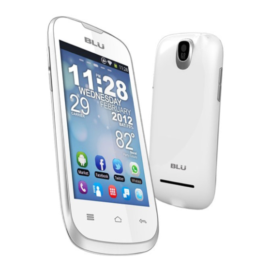
- Page 1 DASH 3.5 SERVICE MANUAL...
- Page 2 ATTENTION Boards, which contain Electrostatic Sensitive Device(ESD), art indicated. Following information is ESD handling: Service personnel should ground themselves by using a wrist strap when exchange system boards. When repairs are made to a system board, they should spread the floor with anti-static mat which is also grounded. Use a suitable, grounded soldering iron.
-
Page 3: Table Of Contents
Contents Contents ............................3 1. Introduction ..........................4 1.1 Objective ..........................4 1.2 General Safety notice ......................4 1.3 Use Instruction ........................4 2. Technology summarize ....................... 5 2.1 Description of main board component map ................5 2.2 MSM7225A circuit system ... -
Page 4: Introduction
1. Introduction 1.1 Objective The manual is not a general publication but only edited for experienced technician. The main purpose is to provide basic foundation for the electrical & mechanical maintenance. 1.2 General Safety notice 1) Only experienced technician can repair with this guide during product is power on. Any maintenance by other non-technicians will cause serious damage of the handset. -
Page 5: Technology Summarize
2. Technology summarize 2.1 Description of main board component map... -
Page 7: Msm7225A Circuit System
2.2 MSM7225A circuit system MSM7225A functional block diagram as following: MSM7225A functional system is made of three parts as below:... -
Page 8: Base Band Circuit
Digital baseband function: Memory, LCM, GPIO interface, Keypad interface etc. Analog baseband function: AUDIO (including MIC, Receiver, Speaker) ,Camera, Video, Ambient light and Proximity sensor, Power management, RTC, Charge control, etc. RF function: RF front-end module, Antenna, RF transceiver, GSM/WCDMA communication system, etc. -
Page 9: Power Management Circuit
3) Higher performance five-stage pipeline, Harvard cached architecture 4) Higher internal CPU clock rate with on-chip cache 5) Internal watchdog and sleep timers ◆ QDSP5000 350 MHz application digital signal processing (ADSP) 1) 512 KB L2 cache ◆ QDSP4000 122.88 MHz modem digital signal processing (MDSP) Memory support features ◆... - Page 10 Power management features: ◆ Linear regulated charging from an external DC charger supply ◆ Four buck switching regulators ◆ One negative charge pump switching regulator ◆ 19 linear regulators ◆ Multiple input ADC ◆ Single sine wave and dual square wave output VCTCXO (or XO) buffers and regulator with deglitches.
-
Page 11: Bt/Fm Circuit
with GSM transmit pulse ◆ PDM flip-flop - built-in voltage leveling and clock synchronization flip-flop 2.5 BT/FM circuit BT/FM schematic as following: WCN2243 integrated BT/FM function. ◆ Standalone BT 2.4 GHz BT transceiver 2) BT baseband processor Compliant with BT core specification version 4.0(BR/EDR+BLE) ◆... -
Page 12: Rf Circuit
2.6 RF circuit RF functional block diagram as following: RF interface features: ◆ TX output chain controls 1) Multiple CDMA and UMTS PA on/off and range controls 2) GSM PA power control 3) 14-bit generic RF controller (GRFC) interface ◆ RTR6285A status and control 1) Multiple SSBIs 2) Tx enable and gain control ◆... -
Page 13: Fail To Charge
Fourth, if the current stay in 40mA, we should check the circuit around flash, when CPU calling program from flash fail, the current will stay in 40mA, re-download the software or change a new flash or CPU. Fail to power on Check if the battery Change is OK. -
Page 14: Fail To Display
No charge Check battery Check battery can power on connector related component normal or not? Change a new Check J1702 solder OK or not? Change T1710 Check T1710 & or C1802 C1802 Check C1008, and Change related R1008 ok or not? component Check U1001 Hot or change... -
Page 15: Fail To Call
No display Is the LCM well? Change LCM Change U1501 reverse or U1501 damaged R0004, R1177 Add R0004 or R1177 NC or not Change Change or U0401 re-solder U0401 3.4 Fail to call When call with somebody, we cannot hear what he says or he cannot hear what we say: This fail may cause by receiver or microphone fail, it can test in factory mode, type“*#*#7#*#*”... -
Page 16: Speaker No Sound
Call 112, if cannot hear voice, it may receiver problem, change a new receiver, check R1916, R1917, C1926, C1927, C1928, C2002, V1201, V1202 ok or not, if ok, check CPU, re- hot U0401 or change a new one. Voice sending or receiving no function Can hear sound in Check RF... - Page 17 No sound Is speaker OK? Replace Speaker Are B1910, B1911 ADD B1910,B1911 NC or not? Check T1912, Re-solder uncorrected T1903, C1929, component C1930, and C2001 ok or not? Hot or change U1001 Check U1001...
-
Page 18: Earphone Fail
3.6 Earphone fail No sound in earphone Is earphone Replace connector OK? earphone Is J601 soldering Re-solder J601 well? Re-solder uncorrected Are All TVS right direction? Re-solder Related R, uncorrected R C C right? Hot or change U1001... -
Page 19: Vibrator Fail
3.7 Vibrator fail Motor doesn’t work Supply 3.3V for motor, Change a test motor can work or new Motor Check related R, C OK Change uncorrected or NOT, Check D1201 component reverses or not Hot U1001 or Change a new one 3.8 Side key fail Side key no function Re-solder or... -
Page 20: Failure To Identify Sim Card
3.9 Failure to identify SIM card SIM is not identified Touch Pin is Clean SIM socket clean? SIM is damaged. Change a new Replace it SIM to try Change a new one. Is SIM socket good? Change U1001 Check if VSIM1/ VSIM2 are OK? Check each signal Hot U1001 or change... -
Page 21: Camera Fail
3.11 Camera fail First, change a new camera module, check camera connector ok or not; Second, check AVDD, DOVDD. Third, use oscilloscope to test I2C, CAM_RST, CAM_MCLK, CAM_PCLK, MIPI_DATA, and MIPI_CLK. If signals abnormal check U0401, re-hot or change a new one. Camera fail Is camera connector Re-solder or... -
Page 22: Failure To Read T-Flash Card
3.12 Failure to read T-flash card First, change another T flash card, check whether T flash card bad or not Second, check card connector solder ok or not, if fail, re-solder or change a new one Third, check TVS reserved or not, check VDD whether normal Fourth, test related signals, such as MCCK, MCCM0, MCDA0, MCDA1…MCDA3, if abnormal, check U0401, re-hot or change a new one. -
Page 23: Bga Related Gnd Or No Function Pad
4. BGA related GND or no function pad Red--------no function pad White------GND pad 4.1 CPU and memory pin map... -
Page 24: Pmu Pin Map
4.2 PMU pin map... -
Page 25: Bt/Fm/Wifi Pin Map
4.3 BT/FM/WIFI pin map...
Need help?
Do you have a question about the DASH 3.5 and is the answer not in the manual?
Questions and answers