Table of Contents
Advertisement
Quick Links
Please note that Cypress is an Infineon Technologies Company.
The document following this cover page is marked as "Cypress" document as this is the
company that originally developed the product. Please note that Infineon will continue
to offer the product to new and existing customers as part of the Infineon product
portfolio.
Continuity of document content
The fact that Infineon offers the following product as part of the Infineon product
portfolio does not lead to any changes to this document. Future revisions will occur
when appropriate, and any changes will be set out on the document history page.
Continuity of ordering part numbers
Infineon continues to support existing part numbers. Please continue to use the
ordering part numbers listed in the datasheet for ordering.
www.infineon.com
Advertisement
Table of Contents

Subscribe to Our Youtube Channel
Related Manuals for Cypress Semiconductor infineon EZ-USB FX3


Summary of Contents for Cypress Semiconductor infineon EZ-USB FX3
- Page 1 Please note that Cypress is an Infineon Technologies Company. The document following this cover page is marked as “Cypress” document as this is the company that originally developed the product. Please note that Infineon will continue to offer the product to new and existing customers as part of the Infineon product portfolio.
-
Page 2: Table Of Contents
AN76405 EZ-USB® FX3™/FX3S™ Boot Options Author: Sai Krishna Vakkantula Associated Part Family: CYUSB30xx Related Application Notes: AN75705 More code examples? We heard you. For a consolidated list of USB SuperSpeed Code Examples, visit http://www.cypress.com/101781 AN76405 describes the boot options—over USB, I C, serial peripheral interface (SPI), and synchronous Address Data FX3™... -
Page 3: Introduction
EZ-USB® FX3™/FX3S™ Boot Options Introduction EZ-USB FX3 is the next-generation USB 3.0 peripheral controller, providing highly integrated and flexible features that enable developers to add USB 3.0 functionality to a wide range of applications. FX3 supports several boot options, including booting over USB, I C, SPI, synchronous and asynchronous ADMux, and asynchronous SRAM interfaces. -
Page 4: Fx3 Boot Options
EZ-USB® FX3™/FX3S™ Boot Options The tool allows users the ability to select from one of five Cypress-supplied interfaces, or choose to create their own GPIF II interface from scratch. Cypress has supplied industry-standard interfaces such as asynchronous and synchronous Slave FIFO, and asynchronous and synchronous SRAM. Designers who already have one of these pre- defined interfaces in their system can simply select the interface of choice, choose from a set of standard parameters such as bus width (x8, 16, x32) endianness, clock settings, and then compile the interface. -
Page 5: Usb Boot
D e f a u l t S i l i c o n I D By default, FX3 has the default Cypress Semiconductor VID=04B4h and PID=00F3h stored in the ROM space. This VID/PID is used for default USB enumeration unless the eFUSE VID/PID is programmed. - Page 6 EZ-USB® FX3™/FX3S™ Boot Options 4 . 2 . 2 B o o t l o a d e r R e vi s i o n The bootloader revision is stored in the ROM area at the address FFFF_0020h, as shown in Table Table 3.
- Page 7 EZ-USB® FX3™/FX3S™ Boot Options 4 . 2 . 9 U S B C h a p t e r 9 a n d V e n d o r C o m m a n d s The FX3 bootloader handles the commands in Table Table 5.
- Page 8 EZ-USB® FX3™/FX3S™ Boot Options Table 8. Command Fields for Transfer of Execution to Program Entry Byte Field Value Description bmRequestType Request type: Bit7: Direction Bit6-0: Recipient bRequest This byte will be A0 for firmware download/upload vendor command. wValue AddrL (LSB) 32-bit Program Entry wIndex AddrH (MSB)
-
Page 9: Checksum Calculation
EZ-USB® FX3™/FX3S™ Boot Options read signature bytes. if (wSignature != 0x5943) // check ‘CY’ signature byte printf(“Invalid image”); return fail; fread(&i, 2, 1, input_file); // skip 2 dummy bytes dCheckSum = 0; while (1) fread(&dLength,4,1,input_file); // read dLength fread(&dAddress,4,1,input_file); // read dAddress if (dLength==0) break;... - Page 10 Device class (No class-specific protocol is implemented.) bDevSubClass Device subclass (No class-specific protocol is implemented.) bDevProtocol Device protocol (No class-specific protocol is implemented.) bMaxPktSize Endpoint0 packet size is 64. wVID 04B4h Cypress Semiconductor VID 10-11 wPID 00F3h FX3 silicon 12-13 wBCDID 0100h FX3 bcdID...
- Page 11 EZ-USB® FX3™/FX3S™ Boot Options Table 10. Device Qualifier Offset Field Value Description bLength Length of this descriptor = 10 bytes bDescType Descriptor type = Device Qualifier wBCDUSB 0200h USB Specification version 2.00 bDevClass Device class (No class-specific protocol is implemented.) bDevSubClass Device subclass (No class-specific protocol is implemented.) bDevProtocol...
-
Page 12: Boot Image Format
EZ-USB® FX3™/FX3S™ Boot Options Table 13. String Descriptors Offset Field Value Description bLength Length of this descriptor = 04 bytes bDescType Descriptor type = String wLanguage 0409h Language = English bLength Length of this descriptor = 16 bytes bDescType Descriptor type = String –... -
Page 13: C Eeprom Boot
EZ-USB® FX3™/FX3S™ Boot Options Binary Image Length Description Header (16-bit) dAddress N Should contain valid Program Entry (Normally, it should be the Startup code, that is, the RESET vector.) Note: If bImageCTL.bit0 = 1, the bootloader will not transfer the execution to this Program Entry. If bImageCTL.bit0 = 0, the bootloader will transfer the execution to this Program Entry. -
Page 14: Features
EZ-USB® FX3™/FX3S™ Boot Options For I C EEPROM boot, the state of the PMODE[2:0] pins should be 1ZZ, as shown in Table Table 15. PMODE Pins for I C Boot PMODE[2] PMODE[1] PMODE[0] The pin mapping of the FX3 I C interface is shown in Table Table 16. - Page 15 EZ-USB® FX3™/FX3S™ Boot Options Figure 4. Pin Connections of a Typical I C EEPROM 5 . 2 . 1 I m p o r t a n t P o i n t s o n 1 2 8 - K B E E P R O M Ad d r e s s i n g In the case of a 128-KB I C EEPROM, the addressing style is not standard across EEPROMs.
-
Page 16: Boot Image Format
EZ-USB® FX3™/FX3S™ Boot Options Boot Image Format The bootloader expects the firmware image file to be in the format shown in Table 19. The EZ-USB FX3 SDK provides a software utility that can be used to generate a firmware image in the format required for I C EEPROM boot. -
Page 17: Checksum Calculation
EZ-USB® FX3™/FX3S™ Boot Options Binary Image Header Length (16-bit) Description dCheckSum The 32-bit unsigned little-endian checksum data will start from the First sections to the termination section. The checksum will not include the dLength, dAddress, and Image Header. Example: The binary image file is stored in the I C EEPROM in the following order: Byte0: “C”... - Page 18 EZ-USB® FX3™/FX3S™ Boot Options Location10: 0xDDCCBBAA //Section 2 starts Location11: 0x11223344 Location12: 0x00000000 //Termination of Image Location13 0x40008000 //Jump to 0x40008000 in FX3 System RAM Location 14: 0x //Check sum (0x12345678 + 0x9ABCDEF1 + 0x23456789 + 6AF37AF2 0xABCDEF12 + 0xDDCCBBAA + 0x11223344) Similarly, you can have N sections of an image stored using one boot image.
-
Page 19: C Eeprom Boot With Usb Fallback
EZ-USB® FX3™/FX3S™ Boot Options C EEPROM Boot with USB Fallback For the I C EEPROM boot with USB fallback, the state of the PMODE[2:0] pins should be Z1Z, as shown in Table Table 20. PMODE Pins for I C Boot with USB Fallback PMODE[2] PMODE[1] PMODE[0]... -
Page 20: Spi Boot
EZ-USB® FX3™/FX3S™ Boot Options SPI Boot Figure 5 shows the system diagram for FX3 when booting over SPI. Figure 5. System Diagram for SPI Boot For SPI boot, the state of the PMODE[2:0] pins should be 0Z1, as shown in Table Table 21. -
Page 21: Selection Of Spi Flash
EZ-USB® FX3™/FX3S™ Boot Options ▪ USB fallback is supported and used for storing new VID/PID information for USB boot. See the SPI Boot with USB Fallback section in this application note for more information. Selection of SPI Flash SPI flash should support the following commands to support FX3 boot. ▪... -
Page 22: Boot Image Format
EZ-USB® FX3™/FX3S™ Boot Options Boot Image Format For SPI boot, the bootloader expects the firmware image file to be in the format shown in Table 23. The EZ-USB FX3 provides a software utility that can be used to generate a firmware image in the format required for SPI boot. Refer to the elf2img utility located in the C:\Program Files\Cypress\EZ-USB FX3 SDK\1.3\util\elf2img directory after installing the SDK. -
Page 23: Checksum Calculation
EZ-USB® FX3™/FX3S™ Boot Options ….. Byte N: Checksum of Image Important Point to Note: Bootloader default boot speed = 10 MHz; to change the speed from 10 MHz to 20 MHz, the bImageCTL[5:4] should be set to 01. Checksum Calculation The bootloader computes the checksum when loading the binary image over SPI. -
Page 24: Spi Boot With Usb Fallback
EZ-USB® FX3™/FX3S™ Boot Options SPI Boot with USB Fallback In all USB fallback (“-->USB”) modes, USB enumeration occurs if 0xB2 boot is selected or an error occurs. After USB enumeration occurs, the external USB Host can boot FX3 using USB boot. SPI boot with USB fallback (SPI --> USB) is also used to store VID and PID for USB boot. -
Page 25: Synchronous Admux Boot
EZ-USB® FX3™/FX3S™ Boot Options Synchronous ADMux Boot Figure 7 shows the FX3 system diagram when booting over the synchronous ADMux interface. Figure 7. System Diagram for Synchronous ADMux Boot External FPGA/ EZ-USB FX3 Processor Sync Sync USB3.0/ ADMux ADMux USB2.0 USB Host PMODE2=Z Bootloader... - Page 26 EZ-USB® FX3™/FX3S™ Boot Options For write operations, both CE# and WE# are asserted. ADV# must be LOW during the address phase of a read/write operation. ADV# must be HIGH during the data phase of a read/write operation. The RDY output signal from the FX3 device indicates that data is valid for read transfers. The pin mapping of the FX3 sync ADMux interface is shown in Table 25.
- Page 27 EZ-USB® FX3™/FX3S™ Boot Options The bootloader allocates 0x500 bytes from 0x1000_0000 – 0x1000_04FF, so 0x1000_0500 – 0x1000_1FFF is available for downloading firmware. When the download application takes over, the memory from 0x1000_0000 – 0x1000_04FF can be used for other purposes. Figure 9.
- Page 28 EZ-USB® FX3™/FX3S™ Boot Options Figure 10. Synchronous ADMux Interface – Write Cycle Timing Notes: The External P-Port processor and FX3S operate on the same clock edge. The External processor sees RDY assert two cycles after WE# asserts and deasserts three cycles after the edge sampling the data.
- Page 29 EZ-USB® FX3™/FX3S™ Boot Options 9 . 1 . 6 G P I F I I AP I P r o t o c o l This protocol is used only in GPIF II boot mode. After reset, the external application processor (AP) communicates with the bootloader using the command protocol defined in Table Table 27.
- Page 30 EZ-USB® FX3™/FX3S™ Boot Options The bootloader does not support queuing commands. Therefore, every time a command is sent, the host must read the response. To prevent the corruption of the API structure during the downloading process ,the host should not download firmware to the reserved bootloader SYSTEM address (0x4000_0000 to 0x4000_23FF).
- Page 31 EZ-USB® FX3™/FX3S™ Boot Options 9 . 1 . 8 P r o c e s s o r P o r t ( P - P o r t ) R e g i s t e r M a p The register list shown in Table 28 indicates how the PP_xxx registers are mapped on the external P-Port address...
- Page 32 EZ-USB® FX3™/FX3S™ Boot Options Note: While performing register access, the most significant bit of the 8-bit address should be 1, notifying FX3 that it is register access operation. Similarly, for performing socket access, the most significant bit should be set to 0. mdelay();...
- Page 33 EZ-USB® FX3™/FX3S™ Boot Options command[1] = 'Y'; command[2] = 0x02; /* Enter boot mode command. */ command[3] = 0x01; /* 1 data block */ /* Print the command block if you like to see it */ for (i=0; i<512; i++) { if (!(i%16)) printf("\n%.3x: ", i);...
- Page 34 EZ-USB® FX3™/FX3S™ Boot Options ▪ PP_DMA_XFER.LONG_TRANSFER. This config bit indicates if long (multibuffer) transfers are enabled. This bit is set by the application processor as part of transfer initiation. ▪ PP_CONFIG.BURSTSIZE and PP_CONFIG.DRQMODE. These config bits define and enable the size of the DMA burst.
- Page 35 EZ-USB® FX3™/FX3S™ Boot Options printf("%s: Fail timeout; Count = 0\n", __func__); return FAIL; /* enable DRQ WMARK_EV for DRQ assert */ IOWR_REG16(PP_DRQR5_MASK, DMA_WMARK_EV); /* Change FX3 FW to single cycle mode */ val = IORD_REG16(PP_CONFIG); val = (val&0xFFF0)|CFGMODE; IOWR_REG16(PP_CONFIG, val); /* Poll for FX3 FW config init ready */ count = 10000;...
- Page 36 EZ-USB® FX3™/FX3S™ Boot Options do { val = IORD_REG16(PP_SOCK_STAT_L); udelay(10); } while(!(val&(0x1<<sck))); /* write to PP_DMA_XFER to configure transfer socket number, rd/wr operation, and long/short xfer modes */ val = (DMA_ENABLE | LONG_TRANSFER | sck); IOWR_REG16(PP_DMA_XFER, val); /* Poll for DMA_READY_EV */ count = 10000;...
-
Page 37: Boot Image Format
EZ-USB® FX3™/FX3S™ Boot Options IOWR_REG16(PP_DMA_XFER, val); printf("DMA read completed ..\n"); return PASS; For troubleshooting the synchronous ADMux boot, please refer to the Appendix B: Troubleshooting Steps for Sync ADMux Boot. Boot Image Format For sync ADMux boot, the bootloader expects the firmware image to be in the format shown in Table EZ-USB FX3 SDK... - Page 38 EZ-USB® FX3™/FX3S™ Boot Options Binary Image Length Description Header (16-bit) dAddress N Should contain valid Program Entry (Normally, it should be the startup code, for example, the RESET vector.) Note: If bImageCTL.bit0 = 1, the bootloader will not transfer the execution to this Program Entry.
-
Page 39: Emmc Boot
EZ-USB® FX3™/FX3S™ Boot Options The following is an example of code for printing the contents of the .img file into an array in ASCII format: #include <stdio.h> #include <stdint.h> int main (int argc, char *argv[]) char *filename = "firmware.img"; FILE *fp; int i = 0;... -
Page 40: Default State Of I/Os During Boot
EZ-USB® FX3™/FX3S™ Boot Options Default State of I/Os During Boot Table 31 shows the default state of the FX3 I/Os for the different boot modes, while the bootloader is executing before application firmware download). Note: The default state of the GPIOs need not be same when FX3 is in reset and after the boot-loader finishes the configuration. -
Page 41: Related Documents
EZ-USB® FX3™/FX3S™ Boot Options Sync ADMux USB Boot C Boot GPIO SPI Boot Default State Boot Default State Default State Default State PMODE[1] I/P PMODE[1] I/P GPIO[31] PMODE[1] I/P to FX3 to FX3 PMODE[1] I/P to FX3 to FX3 PMODE[2] I/P PMODE[2] I/P GPIO[32] PMODE[2] I/P to FX3... -
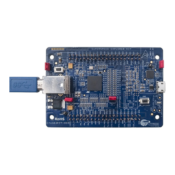
Page 42: A Appendix A: Steps For Booting Using Fx3 Dvk Board (Cyusb3Kit-001)
EZ-USB® FX3™/FX3S™ Boot Options Appendix A: Steps for Booting Using FX3 DVK Board (CYUSB3KIT-001) This appendix describes the stepwise sequence for exercising USB boot, I C boot, and SPI boot using the FX3 DVK board. Figure 12 shows a part of the FX3 DVK board that contains switches and jumpers, which need to be configured appropriately for each boot option. -
Page 43: Usb Boot
EZ-USB® FX3™/FX3S™ Boot Options USB Boot Build the firmware image in the Eclipse IDE as shown in Figure 13, Figure 14. , and Figure 15. . Figure 13. Right-Click on Project in Eclipse IDE www.cypress.com Document No. 001-76405 Rev.*J... - Page 44 EZ-USB® FX3™/FX3S™ Boot Options Figure 14. Select Settings www.cypress.com Document No. 001-76405 Rev.*J...
- Page 45 EZ-USB® FX3™/FX3S™ Boot Options Figure 15. elf2img Command Configuration in Post-Build Steps for USB Boot Image Enable USB boot by setting the PMODE[2:0] pins to Z11. On the DVK board, this is done by configuring the jumpers and switches as shown in Table Table 32.
- Page 46 EZ-USB® FX3™/FX3S™ Boot Options When connected to a USB Host, the FX3 device enumerates in the Control Center as “Cypress USB BootLoader,” as shown in Figure 16. Figure 16. Cypress USB BootLoader Enumeration in Control Center In the Control Center, select the FX3 device by choosing Program > FX3 > RAM, as shown in Figure 17.
-
Page 47: I 2 C Boot
EZ-USB® FX3™/FX3S™ Boot Options Next, browse to the .img file to be programmed into the FX3 RAM. Double-click on the .img file, as shown in Figure Figure 18. Select .img File A “Programming Succeeded” message is displayed on the bottom left of the Control Center, and the FX3 device re-enumerates with the programmed firmware. - Page 48 EZ-USB® FX3™/FX3S™ Boot Options Figure 20. Properties of Fx3BootAppGcc Figure 21. elf2img Command Configuration in Post-Build Steps for I C Boot Image www.cypress.com Document No. 001-76405 Rev.*J...
- Page 49 EZ-USB® FX3™/FX3S™ Boot Options Enable USB boot, by setting the PMODE[2:0] pins to Z11. On the DVK board, this is done by configuring the jumpers and switches as shown in Table 33. Table 33. Jumper Configurations for USB Boot Jumper/Switch Position State of Corresponding PMODE Pin J96 (PMODE0)
- Page 50 EZ-USB® FX3™/FX3S™ Boot Options Figure 23. Choose Program > FX3 > I2C E2PROM Figure 24. FX3 Re-Enumerates as “Cypress USB BootProgrammer” After the FX3 DVK board enumerates as “Cypress USB BootProgrammer,” the Control Center application prompts you to select the firmware binary to download. Browse to the .img file that is to be programmed into the I EEPROM, as shown in Figure 25.
- Page 51 EZ-USB® FX3™/FX3S™ Boot Options Figure 26. I C EEPROM Programming Update in Control Center Change the PMODE pins on the DVK board to Z1Z to enable I C boot. On the DVK board, this is done by configuring the jumpers and switches as shown in Table 34.
-
Page 52: Spi Boot
EZ-USB® FX3™/FX3S™ Boot Options SPI Boot Build the firmware image in the Eclipse IDE as shown in Figure 27. , Figure Figure Figure 27. Right-Click on Project in Eclipse IDE Figure 28. Select “Settings” www.cypress.com Document No. 001-76405 Rev.*J... - Page 53 EZ-USB® FX3™/FX3S™ Boot Options Figure 29. elf2img Command Configuration in Post-Build Steps for SPI Boot Image Enable USB boot by setting the PMODE[2:0] pins to Z11. On the DVK board, this is done by configuring the jumpers and switches as shown in Table Table 35.
- Page 54 EZ-USB® FX3™/FX3S™ Boot Options Figure 30. Cypress USB BootLoader Enumeration in Control Center In the Control Center, select the FX3 device and then choose Program > FX3 > SPI FLASH, as shown in Figure . Browse to the .img file to be programmed into the SPI flash, as shown in Figure Figure 31.
- Page 55 EZ-USB® FX3™/FX3S™ Boot Options Figure 32. Double-Click on the .img File to be Programmed into SPI Flash After programming is complete, the bottom left corner of the window displays “Programming of SPI FLASH Succeeded,” as shown in Figure 33. Figure 33. Successful Programming of SPI Flash Indicated at Bottom Left of Control Center www.cypress.com Document No.
- Page 56 EZ-USB® FX3™/FX3S™ Boot Options Change the PMODE[2:0] pins on the DVK board to 0Z1 to enable SPI boot. On the DVK board, this is done by configuring the jumpers and switches as shown in Table 36. Table 36. Jumper Configurations for SPI Boot Jumper/Switch Position State of Corresponding PMODE Pin...
-
Page 57: B Appendix B: Troubleshooting Steps For Sync Admux Boot
EZ-USB® FX3™/FX3S™ Boot Options Appendix B: Troubleshooting Steps for Sync ADMux Boot This appendix describes the step-wise instructions on how to test and debug various sequences for sync ADmux boot. Initialization Configure the memory interface on the master side to meet FX3’s timing requirements. If required (in cases like Linux), memory-map the address region corresponding to the FX3 interface to a region of virtual memory. -
Page 58: Test Firmware Download
EZ-USB® FX3™/FX3S™ Boot Options Read 512 bytes of data (256 cycles) from the FX3 address 0x02. Verify that the first four bytes contain the pattern 0x57, 0x42, 0x01 (don’t care), and 0x00. Initiate a FIFO read command to read the data from address 0x40003000: Wait until bit 0 of PP_SOCK_STAT_L register (0x9E) is set. - Page 59 EZ-USB® FX3™/FX3S™ Boot Options Now, write the complete firmware content to socket 1, 512 bytes at a time. Follow the procedure given below to write each 512 bytes to socket 1. Wait until bit 1 of the PP_SOCK_STAT_L register (0x9E) is set. Write 0x0301 to the PP_DMA_XFER register (0x8E).
-
Page 60: C Appendix C: Using The Elf2Img Utility To Generate Firmware Image
EZ-USB® FX3™/FX3S™ Boot Options Appendix C: Using the elf2img Utility to Generate Firmware Image This appendix describes how to use the elf2img utility (in the util\elf2img folder in the SDK installation path) to generate the firmware image for boot options mentioned in this application note. Usage The utility is a console application that needs to be invoked with the following options: elf2img.exe -i <elf filename>... -
Page 61: C.1.3.2 Spi Parameters
EZ-USB® FX3™/FX3S™ Boot Options C.1.3.2 SPI Parameters The encoding in the case of SPI boot is as follows: Must be zero. Bits 3 - 1 Don't care Bits 5 - 4 SPI operating frequency [0 = 10 MHz, 1 = 20 MHz, 2 = 30 MHz] Bits 7 - 6 Must be zero. - Page 62 EZ-USB® FX3™/FX3S™ Boot Options Document History FX3™/FX3S™ Boot Options ® Document Title: AN76405 - EZ-USB Document Number: 001-76405 Revision Orig. of Submission Description of Change Change Date 3616262 05/14/2012 New application note 3807283 11/19/2012 Merged the following application notes into AN76405: AN73150, AN70193, AN68914, and AN73304 Clarified the SPI Flash parts tested for boot Added an example for Sync ADMux firmware download implementation...
- Page 63 San Jose, CA 95134-1709 © Cypress Semiconductor Corporation, 2012-2019. This document is the property of Cypress Semiconductor Corporation and its subsidiaries, including Spansion LLC (“Cypress”). This document, including any software or firmware included or referenced in this document (“Software”), is owned by Cypress under the intellectual property laws and treaties of the United States and other countries worldwide.
Need help?
Do you have a question about the infineon EZ-USB FX3 and is the answer not in the manual?
Questions and answers