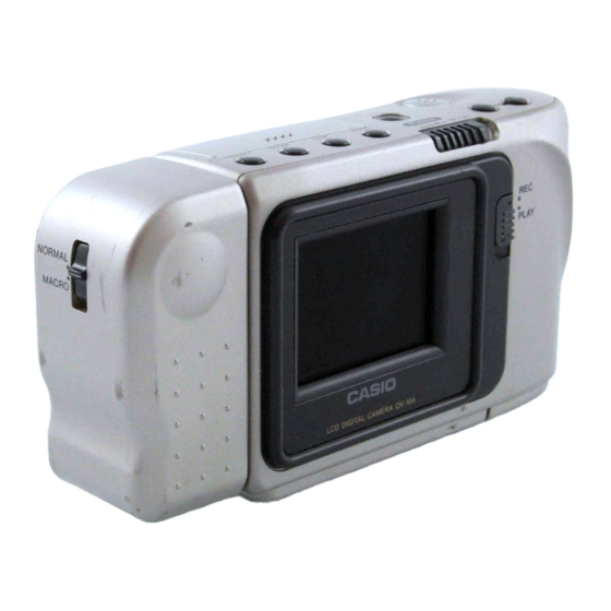
Casio QV-10A Service Manual & Parts List
For pal
Hide thumbs
Also See for QV-10A:
- Service manual & parts list (40 pages) ,
- Owner's manual (23 pages) ,
- Owner's manual (23 pages)
Table of Contents
Advertisement
Quick Links
Advertisement
Table of Contents

Related Manuals for Casio QV-10A


Summary of Contents for Casio QV-10A
- Page 1 (without price) QV-10A (KX-723C) (For PAL) APR. 1996...
-
Page 2: Table Of Contents
CONTENTS SPECIFICATIONS ..................1 BLOCK DIAGRAM ..................2 CIRCUIT OPERATIONS ................3 COLOR ADJUSTMENT ................13 ADJUSTMENT ..................... 15 TROUBLESHOOTING ................. 18 DISASSEMBLY ................... 19 ASSEMBLY ....................20 PRINTED CIRCUIT BOARDS ..............21 EXPLODED VIEW ..................23 PARTS LIST ....................24 SCHEMATIC DIAGRAMS ................ -
Page 3: Specifications
SPECIFICATIONS Item Specification 1. Recording System Digital (JPEG based)/Field recording 2. Video Signal System 3. Recording Medium Built-in 16-Mbit flash memory 4. Number of pages 5. Delete Functions Single page; All pages (with page protect feature) 6. Imaging Device 1/5-inch CCD (Total Number of Pixels: 250,000) 7. -
Page 4: Block Diagram
BLOCK DIAGRAM 1 1 1 1 2 2 2 2 Camera PCB Digital PCB 3 3 3 3 Linear PCB V RAM IC300 HM53812BJ8 IR3P90Y Gate Array HG51B167FB IC400 MSM6770GS Flash Memory 5 5 5 5 TC5816FT-1 VIDEO OUT (Video I/O) D RAM HM514B00 ALJ8... -
Page 5: Circuit Operations
CIRCUIT OPERATIONS CAMERA UNIT (CAMERA PCB) The camera unit is composed a lens, color filter, CCD (IC802), driver (IC800) and signal processor (IC802). It produces voltages R, B, and G, for the colors red, blue, and green when light from a scene is focused on the surface. These voltage values vary according to the intensity of the respective color being scanned. - Page 6 3 CCD (IC802) A charge-coupled device in which charges are introduced when light from a scene is focused on the surface of the device. The image points are accessed sequentially to produce a television-type output signal. Effective picture element: 249,936 = 508 (H) x 492 (V) 532(H) 508(H) PHIS1 ~ PHIS4:...
- Page 7 The color and the luminance data are mixed in the gate array to make the video signal. As to spare parts for digital PCB, Casio supplies PCB ass'y and the individual parts. — 5 —...
- Page 8 1 CPU (IC600) Controls the CCD, D RAM, Flash memory and key operation. PA15 ~ PA0 CS3 ~ CS0, A21 ~ A16 Port A Address RAM1 PROM/MASKROM1 Reset, MD2 ~ MD0, EXTAL, XTAL A15 ~ A0 Direct memory access controller Interrupt User break Direct state controller...
- Page 9 CPU PIN FUNCTION Pin No. Terminal Name I N / O U T Function PB14 Timing pattern output. PB15 — Not used. Ground terminal. 4 - 11 AD0 - AD7 IN/OUT Address bus. Ground terminal. 13 - 14 AD8 - AD9 —...
- Page 10 Pin No. Terminal Name I N / O U T Function 83, 84 Power source. 85, 86 AVCC, AVREF Connected to VCC3. 87 - 89 PC0 - PC2 Key input terminal. Low battery detection terminal. AVSS Ground terminal. 92 - 95 PC4 - PC7 —...
- Page 11 3 V RAM It is used for encoder function. 4 Flash Memory Up to 96 images can be stored in memory. Flash memory does not require electrical power to store data, so image data is retained in memory even when you turn camera power off. If batteries go dead, simply load a set of new batteries or connect the AC adaptor and you will be able to view images in camera memory.
- Page 12 LINEAR PCB IC300 generates the tricolor (red, green and blue) from the video signal, and IC400 controls the TFT-LCD display. Power Supply Terminal Voltage Purpose VCC2 4.3 ~ 4.7 (V) Logic crcuit VCC4 9.5 ~ 11.0 (V) Display VEE2 -7.0 ~ -8.0 (V) Display VEE4 -16.5 ~ -17.9 (V)
- Page 13 IC400 Key control 39 AFTO 46 VREF 45 U1 Analog control 44 VH1 5.9MHz control 43 VL1 Clock 41 OUT Mode control Horizontal control Mode Tuning program Control control VMUTEB VTUCK POCL 34 SW Channel Tuning Up/Down VBAR bar control CK2 Initial counter UBAR...
- Page 14 TFT-LCD Selective period Gate electrode Source electrode Gate Frame period pulse Picture element A t1 t2 t3 Common substrate TFT array substrate Picture Common element electrode V COM Each picture element electrode is controlled by a transistor. To the gate electrodes, the gate pulse is applied timesharing.
-
Page 15: Color Adjustment
Notes: • The support utility disk for QV-10 does not work for QV-10A. • Use an AC adapter for the power source of the QV-10A to avoid the failure of the adjustment. • QV-10A support utility disk is supplied from CASIO. Please contact to Technical Dept., Overseas Service Div. - Page 16 Execution of the color adjustment 1. Set the aperture switch to F8 position, and turn on QV-10A. 2. Put the color filter on the light source, and turn on the light box. Color filter: LBA 3 Light box: Handy 5000 3.
-
Page 17: Adjustment
ADJUSTMENT LINEAR PCB Items to Be Adjusted Item Measuring Instrument VCC2 voltage setting Voltmeter, Regulated power supply VBL voltage setting Voltmeter, Regulated power supply Vcom adjustment Pattern generator, Oscilloscope, Regulated power supply, Photo sensor amp., Band pass filter Free-running Frequency Pattern generator, Oscilloscope, Regulated power supply adjustment Bright and Contrast adjustment... - Page 18 EQUIPMENT CONNECTION / ADJUSTMENT PROCEDURE VCC2 Voltage Setting Regulated QV-10A power Voltmeter supply Input Output DC Jack TP107 5.0 ± 0.05 V Input Input Input Output Output Adjust Result Connection Point Signal Connection Point Adjust for 4.50 ± 0.02 V...
- Page 19 2) Press the self-timer and the DEL button at a time. 3) Press [+] or [–] to select the BLACK. 4) Press the shutter button. 5) Place a photo diode on the middle of the display. QV-10A Photo sensor amp. Oscilloscope Photo...
-
Page 20: Troubleshooting
Bright and Contrast Adjustment Pattern QV-10A VCC2 generator Oscilloscope 10 K CP303 Input Output TP412 TP101 TP410 Trigger Input Input Input Output Output Adjust Result Connection Point Signal Connection Point Adjust VR304 until A in the above diagram equals 3.5 ± 0.1 V. -
Page 21: Disassembly
DISASSEMBLY 1. Remove the two screws on the bottom of the unit. 2. Rotate the camera unit then remove the two screws on the side of the unit. 3. Remove the upper case at the top of the unit. — 19 —... -
Page 22: Assembly
ASSEMBLY When assembling the unit, check the following points. 1. Be sure to align the slide switch on the linear PCB with the switch knob. Upper case Back light Switch knob Linear PCB Slide switch 2. Be sure to align the slide switch on the key PCB with the switch knob. Switch knob Slide switch 3. -
Page 23: Printed Circuit Boards
PRINTED CIRCUIT BOARDS LINEAR R303 C308 C311 C310 VR305 C312 L300 C337 H300 C307 R313 C121 C123 C321 C305 C318 R316 IC300 R319 D103 C303 C322 C301 C125 C300 C325 T100 R301 R320 R110 C326 C338 VR100 R121 R111 L401 IC100 R321 L401... - Page 24 DIGITAL CN601 C548 C731 L601 Q500 L500 L507 IC504 L501 R511 R510 C543 C517 C531 T500 C540 C730 IC505 C544 C545 R509 C523 R517 C546 C542 C541 R605 R606 Q610 IC701 IC601 Q611 CN600 Top View D506 Q612 L735 R614 C519 L600 L540...
-
Page 25: Exploded View
EXPLODED VIEW 20-1-1 20-1 20-3 20-2 20-1-3 20-1-2 19-5 19-4 19-2 19-1 19-3 — 23 —... -
Page 26: Parts List
PARTS LIST LINEAR PCB ASS'Y Item Code No. Parts Name Specification Connectors CN150 3501 9184 Connector CGP1605-0101 CN400 3501 8316 Connector 52559-2090 Diodes D101 7101 1194 Chip diode MA111-(TX) D102 2390 1379 Schottky diode MA729-(TX) D103 2390 1379 Schottky diode MA729-(TX) D104 7101 1194 Chip diode... - Page 27 DIGITAL PCB ASS'Y Item Code No. Parts Name Specification Connectors CN600 3501 9359 Connector 9610S-08Y900 CN602 3501 9198 Connector 52559-1490 CN603 3501 9198 Connector 52559-1490 Diodes D500 2390 2268 Chip diode MA727-(TX) D501 2360 1876 Chip zener diode MA8100-M(TX) D502 2390 1379 Schottky diode MA729-(TX) D503...
- Page 28 Item Code No. Parts Name Specification Q700 2253 0133 Chip transistor 2SD1819A-R(TX) Q701 2251 0189 Chip transistor 2SB1218A-R(TX) Q702 2253 0133 Chip transistor 2SD1819A-R(TX) Converter T500 3701 0693 DC-DC converter CEE98-05 MAIN COMPONENT Item Code No. Parts Name Specification 6610 8680 Display plate A-K723 K411994-3 6610 8651 Upper case A-K723 K110736A-2...
- Page 29 ACCESSORY Item Code No. Parts Name Specification 5860 8085 Wrist strap ST3-340A 6608 9210 Cleaning cloth A-K613 K412004-1 1014 8773 Video cable VC-K723-FC 1014 7835 Soft case SC-720 Notes: Q – Quantity used per unit R – Rank — 27 —...
- Page 30 The following electrical parts will be not supplied from CASIO. (For QV-10A C) C100 10SL10M C409 EMK212F105Z-T C705 GR39CH270J50PT C101 10SL10M C410 GR39Y5V103Z50PT C706 GR39Y5V104Z25PT C110 GR39Y5V103Z50PT C411 GR39Y5V103Z50PT C707 GR39Y5V104Z25PT C111 GR39Y5V104Z25PT C412 GR39Y5V104Z25PT C708 GR39Y5V104Z25PT C112 GR39W5R332K50PT C413 GR39Y5V104Z25PT...
- Page 31 The following electrical parts will be not supplied from CASIO. (For QV-10A C) L643 ACM4532-102-3P-TP R311 ERJ-3GEYF513V R517 ERJ-3GEYJ103V L700 MLF3216E100K-TP R312 ERJ-3GEYK106V R600 ERJ-3GEYJ123V L701 MLF2012E100K-TP R313 ERJ-3GEYJ681V R601 ERJ-3GEYJ123V L702 BK1608HM601-T R314 ERJ-3GEYJ562V R602 ERJ-3GEYJ123V L703 BK1608HM601-T R315 ERJ-3GEYJ822V...
- Page 32 The following electrical parts will be not supplied from CASIO. (For QV-10A C) R903 ERJ-3GEYJ472V R904 ERJ-3GEYJ103V R905 ERJ-3GEYJ273V R906 ERJ-3GEYJ182V R907 ERJ-3GEYJ153V R908 ERJ-3GEYJ102V R909 ERJ-3GEYJ102V R910 ERJ-3GEYJ102V VR100 EVM-1XSX50B53 VR101 EVM-1XSX50B14 VR300 EVM-1XSX50B24 VR302 EVM-1XSX50B54 VR303 EVM-1XSX50B54 VR304 H0614D-10KB...
-
Page 33: Schematic Diagrams
SCHEMATIC DIAGRAMS LINEAR — 31 —... - Page 34 DIGITAL — 32 —...
- Page 35 — 33 —...
-
Page 36: Waveforms
WAVEFORMS 6.4 µsec 6 µsec 6.4 µsec 1 IC100 pin 5 2 Q100 collector 3 IC101 pin 5 6 µsec 64 µsec 64 µsec 5 IC300 pin 9 6 IC300 pin 22 4 Q101 collector 64 µsec 64 µsec 125 µsec 7 IC300 pin 21 8 IC300 pin 41 9 IC300 pins 35, 37, 39... - Page 37 MA0500461A...
Need help?
Do you have a question about the QV-10A and is the answer not in the manual?
Questions and answers