Table of Contents
Advertisement
Quick Links
Advertisement
Table of Contents

Related Manuals for Casio QV-100


Summary of Contents for Casio QV-100
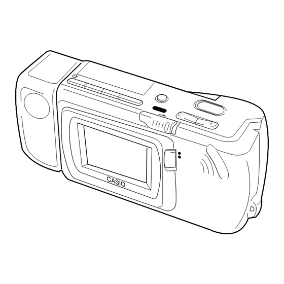
- Page 1 (without price) QV-100 (KX-725B) (For NTSC) AUG. 1996...
-
Page 2: Table Of Contents
CONTENTS SPECIFICATIONS ..................1 BLOCK DIAGRAM ..................2 FLOW DIAGRAM ................... 3 POWER SUPPLY CIRCUIT OPERATION ............. 5 TROUBLESHOOTING ................... 8 DISASSEMBLY ....................9 PRINTED CIRCUIT BOARDS ..............11 EXPLODED VIEW ..................13 PARTS LIST ....................14 SCHEMATIC DIAGRAMS ................21 WAVEFORMS .................... -
Page 3: Specifications
SPECIFICATIONS Item Specification 1. Recording System Digital (JPEG based)/Field recording 2. Video Signal System NTSC 3. Recording Medium Built-in 32-Mbit flash memory 4. Number of pages FINE (VGA) : 64 (approximately 480-kbit compressed) NORMAL (Quarter-VGA) : 192 (approximately 160-kbit compressed) 5. -
Page 4: Block Diagram
BLOCK DIAGRAM Camera Unit Digital PCB IC702 IC701 µPD6461GS Lens µPD482445LGW converter On screen 4Mbit VRAM display Video VRAM encoder contoroller IC703 LC99092-Z03 8 bit to 16 bit Video out converter converter Color processor Data Linear PCB compressor expander IC700 HG51D291FE IC300 IR3P90Y1... -
Page 5: Flow Diagram
FLOW DIAGRAM REC mode IC703 IC700 Converter LC99092-Z03 HG51D291FE Camera Unit IC701 µPD482445LGW IC602 KM29V32000T IC600 HD6437042Y02F IC601 HM51W4260 Digital PCB 1 Exposure and Analog to Digital conversion by Camera unit 2 8 to 16 bits conversion by IC703 3 Storage for work 4 Color processing by IC703: Ye,Cy, Gr →... - Page 6 1 Exposure and Analog to Digital conversion by Camera unit 2 8 to 16 bits conversion by IC703 3 Storage for work 4 Color processing by IC703: Ye, Cy, Gr → Y, By, Ry 5 Storage for work 6 Compression by IC700 7 Storage for work 8 Storage to Flash memory PLAY mode...
-
Page 7: Power Supply Circuit Operation
POWER SUPPLY CIRCUIT OPERATION 2 APO from Pin 42 of IC600 VCC1 R515 Q514 IC507 FU500 R516 C523 C548 C531 6 Voltage detection signal VCC3-1 VCC1 C520 3 POB to Pin102 Q503 of IC600 R511 R512 CN601 Q513 KEY0 R513 KEY2 1 PON from Key PCB... - Page 8 Operation IC505 NAND gate IC506 Flip-flop IC507 Voltage detector Pin 2 (VDD) Pin 1 (OUT) > 3.2 V < 3.2 V Time Chart Power on Power off H (VCC1) H (VCC1) 1. PON 1. PON 2. APO 2. APO H (VCC3) H (VCC3) 3.
- Page 9 Power off by APO Power off by low voltage detection H (VCC1) H (VCC1) 1. PON 1. PON H (VCC3) 2. APO 2. APO H (VCC3) H (VCC3) 3. POB 3. POB 4. FACT 4. FACT H (VCC1) H (VCC1) 5.
-
Page 10: Troubleshooting
TROUBLESHOOTING No Display 1. Check the fuse (FU500) on the digital PCB. 2. Check the fuse (FU100) on the linear PCB. 3. Check the jack (JK500) on the digital PCB. 4. Check the power switch (SW900) on the key PCB. 5. -
Page 11: Disassembly
DISASSEMBLY To disassemble the main unit 1. Open the battery cover, then unhook and remove the grip. Grip Hook 2. Remove the screw. Screw 3. Rotate the camera unit then remove the two screws on the side of the unit. Screw Screw —... - Page 12 4. Remove the two screws on the bottom of the unit. Screw Screw 5. Remove the battery cover and the upper case at the bottom of the unit. 6. Remove the upper case at the top of the unit. Hook Hook To disassemble the camera unit Remove the screw and the camera case.
-
Page 13: Printed Circuit Boards
PRINTED CIRCUIT BOARDS LINEAR C311 C310 C337 C336 C334 R313 C312 L300 R335 R334 C307 C318 C321 D101 L303 IC300 R317 R301 T100 C322 R319 R110 VR100 C333 R111 R424 C348 C347 Q401 IC100 R142 C415 VR101 D105 C150 R333 C416 C409 R403... -
Page 14: Top View
DIGITAL R519 CN601 L540 L514 L704 L643 L502 L512 IC605 C731 C537 C540 C548 IC703 C543 L509 R541 Q508 R625 C547 C500 R626 C730 C542 C625 C629 L641 L503 R517 C551 C546 C541 Q514 R509 R605 R606 C607 Q512 Q611 Q610 C523 IC601... -
Page 15: Exploded View
EXPLODED VIEW 30-1 30-1-2 30-1-1 14-1 18-2 18-1 18-4 18-3 14-1 — 13 —... -
Page 16: Parts List
PARTS LIST LINEAR PCB ASS'Y Item Code No. Parts Name Specification Diodes D101 7101 1194 Chip diode MA111-(TX) D102 2390 1379 Schottoky diode MA729-(TX) D103 2390 1379 Schottoky diode MA729-(TX) D104 7101 1194 Chip diode MA111-(TX) D105 2390 1379 Schottoky diode MA729-(TX) D106 2360 2359 Chip zener diode... - Page 17 DIGITAL PCB ASS'Y Item Code No. Parts Name Specification Diodes D500 2390 2268 Chip diode MA727-(TX) D501 2390 1379 Schottoky diode MA729-(TX) D502 2390 1379 Schottoky diode MA729-(TX) D504 2390 2261 Chip diode MA720-(TX) D505 2390 2261 Chip diode MA720-(TX) D506 2390 1421 Chip schottoky diode MA738-(TX)
- Page 18 Item Code No. Parts Name Specification Q510 7911 0126 Digital transistor DTC144EUAT106 Q511 7911 0126 Digital transistor DTC144EUAT106 Q512 7911 0126 Digital transistor DTC144EUAT106 Q513 7911 0126 Digital transistor DTC144EUAT106 Q514 7911 0126 Digital transistor DTC144EUAT106 Q609 7911 0126 Digital transistor DTC144EUAT106 Q610 2259 2205 Digital transistor...
- Page 19 KEY PCB ASS'Y Item Code No. Parts Name Specification Switches SW900 3412 2002 Slide switch SPVC2-1-T SW901 3412 1995 Switch SKQRAA-T SW902 3412 1995 Switch SKQRAA-T SW903 3412 1995 Switch SKQRAA-T SW904 3412 1995 Switch SKQRAA-T SW905 3412 1995 Switch SKQRAA-T SW906 3412 1995 Switch...
- Page 20 MAIN COMPONENT Item Code No. Parts Name Specification 6611 4510 Display frame K725AAA R340023-1 6611 4710 Adhesive tape E-K725AAA R340051-4 6611 4720 Adhesive tape F-K725AAA R340051-5 6611 4400 REC/PLAY knob K725AAA R340025-1 6611 4410 Spring K725AAA R440045-1 6611 4420 Power switch knob K725AAA R340033-1 6611 4430 Upper case K725AAA R140003-1...
- Page 21 ACCESSORY I t e m Code No. Parts Name Specification 5861 2110 Wrist strap ST-K724 6608 9210 Cleaning cloth A-K613 K412004-1 1014 8773 Video cable VC-K723-FC 1014 9298 Soft case SC-725 Notes: Q – Quantity used per unit R – Rank —...
-
Page 22: Schematic Diagrams
SCHEMATIC DIAGRAMS LINEAR Display Controller Chroma IC Power Supply for LCD Power Supply for Back Light — 20 —... - Page 23 DIGITAL Data Expander Data Compressor Video Encoder Flash Memory 8 to 16 bits Converter Color processor DRAM On Screen Display 5 V Booster Circuit 5 V Power Supply Circuit VRAM 20 V Power Supply Circuit 3.5 V 20 V -10 V 3.5 V Power Supply Circuit -10 V Power Supply Circuit —...
- Page 24 — 22 —...
-
Page 25: Waveforms
WAVEFORMS 4 µsec 4 µsec 4 µsec 1 IC100 pin 5 2 Q100 collector 3 IC101 pin 5 63.5 µsec 4 µsec 63.5 µsec 5 IC300 pin 10 6 IC300 pin 20 4 Q101 collector 63.5 µsec 63.5 µsec 125 µsec 7 IC300 pin 21 9 IC300 pin 36 8 IC300 pin 39... - Page 26 MA1000361A...
Need help?
Do you have a question about the QV-100 and is the answer not in the manual?
Questions and answers