Table of Contents
Advertisement
Quick Links
Advertisement
Table of Contents

Related Manuals for Supermicro X11SDW-4C-TP13F


Summary of Contents for Supermicro X11SDW-4C-TP13F
- Page 1 X11SDW-4C/8C/16C-TP13F USER MANUAL Revision 1.0---Draft 3...
- Page 2 State of California, USA. The State of California, County of Santa Clara shall be the exclusive venue for the resolution of any such disputes. Supermicro's total liability for all claims will not exceed the price paid for the hardware product.
- Page 3 LAN ports, and an onboard TPM 2.0 module. Please note that this motherboard is intended to be installed and serviced by professional technicians only. For processor/memory updates, please refer to our website at http://www.supermicro.com/products/. Manual Organization Chapter 1 describes the features, specifications and performance of the motherboard, and provides detailed information on the processor.
- Page 4 Super X11SDW-4C/8C/16C-TP13F User's Manual Contacting Supermicro Headquarters Address: Super Micro Computer, Inc. 980 Rock Ave. San Jose, CA 95131 U.S.A. Tel: +1 (408) 503-8000 Fax: +1 (408) 503-8008 Email: marketing@supermicro.com (General Information) support@supermicro.com (Technical Support) Website: www.supermicro.com Europe Address: Super Micro Computer B.V.
-
Page 5: Table Of Contents
Preface Table of Contents Chapter 1 Introduction 1.1 Checklist ..........................8 Quick Reference .......................11 Quick Reference Table ......................12 Motherboard Features .......................14 1.2 Processor Overview ......................17 1.3 Special Features ........................17 Recovery from AC Power Loss ..................17 1.4 System Health Monitoring ....................18 Onboard Voltage Monitors ....................18 Fan Status Monitor with Firmware Control ...............18 Environmental Temperature Control .................18 System Resource Alert......................18... - Page 6 Super X11SDW-4C/8C/16C-TP13F User's Manual 2.5 Front Control Panel ......................29 2.6 Connectors and Headers ....................33 2.7 Jumper Settings .........................47 How Jumpers Work ......................47 2.8 LED Indicators ........................54 Chapter 3 Troubleshooting 3.1 Troubleshooting Procedures ....................57 Before Power On ......................57 No Power ..........................57 No Video ...........................57 System Boot Failure ......................58 Memory Errors ........................58...
- Page 7 Preface Appendix D UEFI BIOS Recovery D.1 Overview ..........................72 D.2 Recovering the UEFI BIOS Image ..................72 D.3 Recovering the Main BIOS Block with a USB Device ............73...
-
Page 8: Chapter 1 Introduction
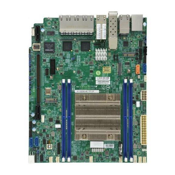
Introduction Congratulations on purchasing your computer motherboard from an acknowledged leader in the industry. Supermicro boards are designed with the utmost attention to detail to provide you with the highest standards in quality and performance. Please check that the following items have all been included with your motherboard. If anything listed here is damaged or missing, contact your retailer. - Page 9 Chapter 1: Introduction Figure 1-1. X11SDW-16C-TP13F Motherboard Image...
- Page 10 Super X11SDW-4C/8C/16C-TP13F User's Manual Figure 1-2. X11SDW-4C-TP13F Motherboard Layout (not drawn to scale) PRESS FIT LED2 JBM2 JSXB1A LED3 COM1 USB 4/5 LAN 2/3/4/5/6/7/8/9 LAN 1 IPMI_LAN LAN 10/11 JPL1 LEDM1 JSDP3 JPI2C1 JLANLED1 JTGLED2 LAN 12/13 JBM1 JMD3:M.2-P PCI-E 3.0 X1...
-
Page 11: Quick Reference
JMD1_SRW1 JMD1 COM2 JSD1 JMD1: M.2-H JVRM1 PCI-E 3.0 X4 / I-SATA4 JRK1 JMD2_SRW1 JPG1 BAR CODE JSDP1 JPL2 DESIGNED IN USA JSIM1 X11SDW-4C-TP13F JSIM1 JSDP2 REV:1.01 JPL3 JPV1 JPL2: JSXB1B LAN 2/3/4/5 1-2:ENABLE 2-3:DISABLE JPL3: LAN 6/7/8/9 1-2:ENABLE JMD2... -
Page 12: Quick Reference Table
Super X11SDW-4C/8C/16C-TP13F User's Manual Quick Reference Table Jumper Description Default Setting M.2 SMBus Enable/Disable Pins 1-2 (Enabled) JBM1 Share LAN Enable/Disable Open: Normal JBM2 Dedicated LAN Enable/Disable Open: Normal JBT1 CMOS Clear Open: Normal C1/JI SMB to PCI-E Slots Enable/Disable Pins 2-3 (Disabled) JPG1 VGA Enable/Disable... - Page 13 Chapter 1: Introduction Connector Description JNVI2C1 Non-volatile Memory (NVMe) I C Header or VPP Header for NVMe Add-on Cards JPH1 4-pin HDD Power Connector Power I C System Management Bus (Power SMB) Header JPV1 8-pin DC Power Connector JPW1 GPU Power Connector JPWR1 24-pin ATX Power Connector JRK1...
-
Page 14: Motherboard Features
Super X11SDW-4C/8C/16C-TP13F User's Manual Motherboard Features Motherboard Features • Intel Xeon D-2100 SoC processor Memory • Supports up to 256GB of ECC RDIMM or 512GB of ECC LRDIMM DDR4 memory with speeds of up to 2400MHz. DIMM Size • Up to 128GB Expansion Slots •... - Page 15 Note 1: The CPU maximum thermal design power (TDP) is subject to chassis and heatsink cooling restrictions. For proper thermal management, please check the chas- sis and heatsink specifications for proper CPU TDP sizing. Note 2: For IPMI configuration instructions, please refer to the Embedded IPMI Con- figuration User's Guide available at http://www.supermicro.com/support/manuals/.
- Page 16 Super X11SDW-4C/8C/16C-TP13F User's Manual Figure 1-3. Chipset Block Diagram Note: This is a general block diagram and may not exactly represent the features on your motherboard. See the previous pages for the actual specifications of your moth- erboard.
-
Page 17: Processor Overview
Chapter 1: Introduction 1.2 Processor Overview The Intel Xeon D-2100 series SoC processor family, with up to 16 cores and up to 100W of power, offers performance, reliability, and high intelligence. As a low-power system-on-a-chip motherboard, the X11SDW-4C/8C/16C-TP13F is optimized for a variety of workloads that requires high compute power in a compact form-factor. -
Page 18: System Health Monitoring
Super X11SDW-4C/8C/16C-TP13F User's Manual 1.4 System Health Monitoring The motherboard has an onboard Baseboard Management Controller (BMC) chip that supports system health monitoring. Onboard Voltage Monitors The onboard voltage monitor will continuously scan crucial voltage levels. Once a voltage becomes unstable, it will give a warning or send an error message to the screen. Users can adjust the voltage thresholds to define the sensitivity of the voltage monitor. -
Page 19: Power Supply
Chapter 1: Introduction In addition to enabling operating system-directed power management, ACPI also provides a generic system event mechanism for Plug and Play, and an operating system-independent interface for configuration control. ACPI leverages the Plug and Play BIOS data structures, while providing a processor architecture-independent implementation that is compatible with Windows 2012/R2 and 2016 Server operating systems. -
Page 20: Chapter 2 Installation
Super X11SDW-4C/8C/16C-TP13F User's Manual Chapter 2 Installation 2.1 Static-Sensitive Devices Electrostatic Discharge (ESD) can damage electronic com ponents. To prevent damage to your motherboard, it is important to handle it very carefully. The following measures are generally sufficient to protect your equipment from ESD. Precautions •... -
Page 21: Motherboard Installation
PCI-E 3.0 X1 JTGLED1 JVGA1 COM2 JMD3_SRW1 JMD1_SRW1 JMD1: M.2-H PCI-E 3.0 X4 / I-SATA4 JMD2_SRW1 BAR CODE DESIGNED IN USA JSIM1 X11SDW-4C-TP13F REV:1.01 JPL2: LAN 2/3/4/5 1-2:ENABLE 2-3:DISABLE JPL3: LAN 6/7/8/9 1-2:ENABLE 2-3:DISABLE JMD2:M.2-H PCI-E 3.0 X2 / S-SATA4... -
Page 22: Installing The Motherboard
Super X11SDW-4C/8C/16C-TP13F User's Manual Installing the Motherboard 1. Locate the mounting holes on the motherboard. See the previous page for the location. 2. Locate the matching mounting holes on the chassis. Align the mounting holes on the motherboard against the mounting holes on the chassis. 3. -
Page 23: Memory Support And Population
Chapter 2: Installation 2.3 Memory Support and Population Important: Exercise extreme care when installing or removing DIMM modules to pre- vent any possible damage. Memory Support The X11SDW-4C/8C/16C-TP13F motherboard supports up to 256GB of ECC RDIMM or 512GB of ECC LRDIMM DDR4 memory in four memory slots. Populating these DIMM slots with memory modules of the same type and size will result in interleaved memory, which will improve memory performance. -
Page 24: Dimm Module Population Sequence
PCI-E 3.0 X1 JTGLED1 JVGA1 COM2 JMD3_SRW1 JMD1_SRW1 JMD1: M.2-H PCI-E 3.0 X4 / I-SATA4 JMD2_SRW1 BAR CODE DESIGNED IN USA JSIM1 X11SDW-4C-TP13F REV:1.01 JPL2: LAN 2/3/4/5 1-2:ENABLE 2-3:DISABLE JPL3: LAN 6/7/8/9 DIMMA1 1-2:ENABLE 2-3:DISABLE JMD2:M.2-H PCI-E 3.0 X2 / S-SATA4... -
Page 25: Dimm Installation
JMD1_SRW1 modules of the same type and speed. JMD1: M.2-H PCI-E 3.0 X4 / I-SATA4 JMD2_SRW1 BAR CODE DESIGNED IN USA JSIM1 X11SDW-4C-TP13F 2. Push the release tabs outwards on both REV:1.01 JPL2: LAN 2/3/4/5 1-2:ENABLE 2-3:DISABLE JPL3: LAN 6/7/8/9... -
Page 26: Rear I/O Ports
PCI-E 3.0 X1 JTGLED1 JVGA1 COM2 JMD3_SRW1 JMD1_SRW1 JMD1: M.2-H PCI-E 3.0 X4 / I-SATA4 JMD2_SRW1 BAR CODE DESIGNED IN USA JSIM1 X11SDW-4C-TP13F REV:1.01 JPL2: LAN 2/3/4/5 1-2:ENABLE 2-3:DISABLE JPL3: LAN 6/7/8/9 1-2:ENABLE 2-3:DISABLE JMD2:M.2-H PCI-E 3.0 X2 / S-SATA4... - Page 27 PCI-E 3.0 X1 JTGLED1 JVGA1 COM2 JMD3_SRW1 JMD1_SRW1 JMD1: M.2-H PCI-E 3.0 X4 / I-SATA4 JMD2_SRW1 BAR CODE DESIGNED IN USA JSIM1 X11SDW-4C-TP13F REV:1.01 JPL2: LAN 2/3/4/5 1-2:ENABLE 2-3:DISABLE JPL3: LAN 6/7/8/9 1-2:ENABLE 2-3:DISABLE JMD2:M.2-H PCI-E 3.0 X2 / S-SATA4...
- Page 28 PCI-E 3.0 X1 JTGLED1 JVGA1 COM2 JMD3_SRW1 JMD1_SRW1 JMD1: M.2-H PCI-E 3.0 X4 / I-SATA4 JMD2_SRW1 BAR CODE DESIGNED IN USA JSIM1 X11SDW-4C-TP13F REV:1.01 JPL2: LAN 2/3/4/5 1-2:ENABLE 2-3:DISABLE JPL3: LAN 6/7/8/9 1-2:ENABLE 2-3:DISABLE JMD2:M.2-H PCI-E 3.0 X2 / S-SATA4...
-
Page 29: Front Control Panel
JF1 contains header pins for various buttons and indicators that are normally located on a control panel at the front of the chassis. These connectors are designed specifically for use with Supermicro chassis. See the figure below for the descriptions of the front control panel buttons and LED indicators. - Page 30 Super X11SDW-4C/8C/16C-TP13F User's Manual Power Button The Power Button connection is located on pins 1 and 2 of JF1. Momentarily contacting both pins will power on/off the system. This button can also be configured to function as a suspend button (with a setting in the BIOS - see Chapter 4). To turn off the power in the suspend mode, press the button for at least seconds seconds.
- Page 31 Chapter 2: Installation Overheat (OH)/Fan Fail Connect an LED cable to OH/Fan Fail connections on pins 7 and 8 of JF1 to provide warnings for chassis overheat and fan failure. Refer to the table below for pin definitions. OH/Fan Fail LED OH/Fan Fail Indicator Pin Definitions (JF1) Pin Definitions...
- Page 32 Super X11SDW-4C/8C/16C-TP13F User's Manual HDD LED The HDD LED connection is located on pins 13 and 14 of JF1. Attach a cable here to show hard drive activity status. Refer to the table below for pin definitions. HDD LED Pin Definitions (JF1) Pins Definition +3.3V...
-
Page 33: Connectors And Headers
PCI-E 3.0 X1 JTGLED1 JVGA1 COM2 JMD3_SRW1 JMD1_SRW1 JMD1: M.2-H PCI-E 3.0 X4 / I-SATA4 JMD2_SRW1 BAR CODE DESIGNED IN USA JSIM1 X11SDW-4C-TP13F REV:1.01 JPL2: LAN 2/3/4/5 1-2:ENABLE 2-3:DISABLE JPL3: LAN 6/7/8/9 1-2:ENABLE 2-3:DISABLE JMD2:M.2-H PCI-E 3.0 X2 / S-SATA4... - Page 34 PCI-E 3.0 X1 JTGLED1 JVGA1 COM2 JMD3_SRW1 JMD1_SRW1 JMD1: M.2-H PCI-E 3.0 X4 / I-SATA4 JMD2_SRW1 BAR CODE DESIGNED IN USA JSIM1 X11SDW-4C-TP13F REV:1.01 JPL2: LAN 2/3/4/5 1-2:ENABLE 2-3:DISABLE JPL3: LAN 6/7/8/9 1-2:ENABLE 2-3:DISABLE JMD2:M.2-H PCI-E 3.0 X2 / S-SATA4...
- Page 35 6. FANB COM2 JMD3_SRW1 JMD1_SRW1 7. Chassis Intrusion JMD1: M.2-H PCI-E 3.0 X4 / I-SATA4 JMD2_SRW1 BAR CODE DESIGNED IN USA JSIM1 X11SDW-4C-TP13F REV:1.01 JPL2: LAN 2/3/4/5 1-2:ENABLE 2-3:DISABLE JPL3: LAN 6/7/8/9 1-2:ENABLE 2-3:DISABLE JMD2:M.2-H PCI-E 3.0 X2 / S-SATA4...
- Page 36 6. JMD2 - M.2 B-Key COM2 JMD3_SRW1 JMD1_SRW1 7. JMD3 - M.2 M-Key JMD1: M.2-H PCI-E 3.0 X4 / I-SATA4 JMD2_SRW1 BAR CODE DESIGNED IN USA JSIM1 X11SDW-4C-TP13F REV:1.01 JPL2: LAN 2/3/4/5 1-2:ENABLE 2-3:DISABLE JPL3: LAN 6/7/8/9 1-2:ENABLE 2-3:DISABLE JMD2:M.2-H PCI-E 3.0 X2 / S-SATA4...
- Page 37 PCI-E 3.0 X1 JTGLED1 JVGA1 COM2 JMD3_SRW1 JMD1_SRW1 JMD1: M.2-H PCI-E 3.0 X4 / I-SATA4 JMD2_SRW1 BAR CODE DESIGNED IN USA JSIM1 X11SDW-4C-TP13F REV:1.01 JPL2: LAN 2/3/4/5 1-2:ENABLE 2-3:DISABLE JPL3: LAN 6/7/8/9 1-2:ENABLE 2-3:DISABLE JMD2:M.2-H PCI-E 3.0 X2 / S-SATA4...
- Page 38 PCI-E 3.0 X1 JTGLED1 JVGA1 COM2 JMD3_SRW1 JMD1_SRW1 JMD1: M.2-H PCI-E 3.0 X4 / I-SATA4 JMD2_SRW1 BAR CODE DESIGNED IN USA JSIM1 X11SDW-4C-TP13F REV:1.01 JPL2: LAN 2/3/4/5 1-2:ENABLE 2-3:DISABLE JPL3: LAN 6/7/8/9 1-2:ENABLE 2-3:DISABLE JMD2:M.2-H PCI-E 3.0 X2 / S-SATA4...
- Page 39 PCI-E 3.0 X1 JTGLED1 JVGA1 COM2 JMD3_SRW1 JMD1_SRW1 JMD1: M.2-H PCI-E 3.0 X4 / I-SATA4 JMD2_SRW1 BAR CODE DESIGNED IN USA JSIM1 X11SDW-4C-TP13F REV:1.01 JPL2: LAN 2/3/4/5 1-2:ENABLE 2-3:DISABLE JPL3: LAN 6/7/8/9 1-2:ENABLE 2-3:DISABLE JMD2:M.2-H PCI-E 3.0 X2 / S-SATA4...
- Page 40 PCI-E 3.0 X1 JTGLED1 JVGA1 COM2 JMD3_SRW1 JMD1_SRW1 JMD1: M.2-H PCI-E 3.0 X4 / I-SATA4 JMD2_SRW1 BAR CODE DESIGNED IN USA JSIM1 X11SDW-4C-TP13F REV:1.01 JPL2: LAN 2/3/4/5 1-2:ENABLE 2-3:DISABLE JPL3: LAN 6/7/8/9 1-2:ENABLE 2-3:DISABLE JMD2:M.2-H PCI-E 3.0 X2 / S-SATA4...
- Page 41 PCI-E 3.0 X1 JTGLED1 JVGA1 COM2 JMD3_SRW1 JMD1_SRW1 JMD1: M.2-H PCI-E 3.0 X4 / I-SATA4 JMD2_SRW1 BAR CODE DESIGNED IN USA JSIM1 X11SDW-4C-TP13F REV:1.01 JPL2: LAN 2/3/4/5 1-2:ENABLE 2-3:DISABLE JPL3: LAN 6/7/8/9 1-2:ENABLE 2-3:DISABLE JMD2:M.2-H PCI-E 3.0 X2 / S-SATA4...
- Page 42 Clock NVMe I C Header JNVI C1 is a management header for the Supermicro AOC NVMe PCI-E peripheral cards. Connect a corresponding I C cable to this header. Refer to the table below for pin definitions. NVMe I C Header...
- Page 43 PCI-E 3.0 X1 JTGLED1 JVGA1 COM2 JMD3_SRW1 JMD1_SRW1 JMD1: M.2-H PCI-E 3.0 X4 / I-SATA4 JMD2_SRW1 BAR CODE DESIGNED IN USA JSIM1 X11SDW-4C-TP13F REV:1.01 JPL2: LAN 2/3/4/5 1-2:ENABLE 2-3:DISABLE JPL3: LAN 6/7/8/9 1-2:ENABLE 2-3:DISABLE JMD2:M.2-H PCI-E 3.0 X2 / S-SATA4...
- Page 44 PCI-E 3.0 X1 JTGLED1 JVGA1 COM2 JMD3_SRW1 JMD1_SRW1 JMD1: M.2-H PCI-E 3.0 X4 / I-SATA4 JMD2_SRW1 BAR CODE DESIGNED IN USA JSIM1 X11SDW-4C-TP13F REV:1.01 JPL2: LAN 2/3/4/5 1-2:ENABLE 2-3:DISABLE JPL3: LAN 6/7/8/9 1-2:ENABLE 2-3:DISABLE JMD2:M.2-H PCI-E 3.0 X2 / S-SATA4...
- Page 45 PCI-E 3.0 X1 JTGLED1 JVGA1 COM2 JMD3_SRW1 JMD1_SRW1 JMD1: M.2-H PCI-E 3.0 X4 / I-SATA4 JMD2_SRW1 BAR CODE DESIGNED IN USA JSIM1 X11SDW-4C-TP13F REV:1.01 JPL2: LAN 2/3/4/5 1-2:ENABLE 2-3:DISABLE JPL3: LAN 6/7/8/9 1-2:ENABLE 2-3:DISABLE JMD2:M.2-H PCI-E 3.0 X2 / S-SATA4...
- Page 46 PCI-E 3.0 X1 JTGLED1 JVGA1 COM2 JMD3_SRW1 JMD1_SRW1 JMD1: M.2-H PCI-E 3.0 X4 / I-SATA4 JMD2_SRW1 BAR CODE DESIGNED IN USA JSIM1 X11SDW-4C-TP13F REV:1.01 JPL2: LAN 2/3/4/5 1-2:ENABLE 2-3:DISABLE JPL3: LAN 6/7/8/9 1-2:ENABLE 2-3:DISABLE JMD2:M.2-H PCI-E 3.0 X2 / S-SATA4...
-
Page 47: Jumper Settings
Chapter 2: Installation 2.7 Jumper Settings How Jumpers Work To modify the operation of the motherboard, jumpers can be used to choose between optional settings. Jumpers create shorts between two pins to change the function of the connector. Pin 1 is identified with a square solder pad on the printed circuit board. See the diagram below for an example of jumping pins 1 and 2. - Page 48 PCI-E 3.0 X1 JTGLED1 JVGA1 COM2 JMD3_SRW1 JMD1_SRW1 JMD1: M.2-H PCI-E 3.0 X4 / I-SATA4 JMD2_SRW1 BAR CODE DESIGNED IN USA JSIM1 X11SDW-4C-TP13F REV:1.01 JPL2: LAN 2/3/4/5 1-2:ENABLE 2-3:DISABLE JPL3: LAN 6/7/8/9 1-2:ENABLE 2-3:DISABLE JMD2:M.2-H PCI-E 3.0 X2 / S-SATA4...
- Page 49 PCI-E 3.0 X1 JTGLED1 JVGA1 COM2 JMD3_SRW1 JMD1_SRW1 JMD1: M.2-H PCI-E 3.0 X4 / I-SATA4 JMD2_SRW1 BAR CODE DESIGNED IN USA JSIM1 X11SDW-4C-TP13F REV:1.01 JPL2: LAN 2/3/4/5 1-2:ENABLE 2-3:DISABLE JPL3: LAN 6/7/8/9 1-2:ENABLE 2-3:DISABLE JMD2:M.2-H PCI-E 3.0 X2 / S-SATA4...
- Page 50 PCI-E 3.0 X1 JTGLED1 JVGA1 COM2 JMD3_SRW1 JMD1_SRW1 JMD1: M.2-H PCI-E 3.0 X4 / I-SATA4 JMD2_SRW1 BAR CODE DESIGNED IN USA JSIM1 X11SDW-4C-TP13F REV:1.01 JPL2: LAN 2/3/4/5 1-2:ENABLE 2-3:DISABLE JPL3: LAN 6/7/8/9 1-2:ENABLE 2-3:DISABLE JMD2:M.2-H PCI-E 3.0 X2 / S-SATA4...
- Page 51 PCI-E 3.0 X1 JTGLED1 JVGA1 COM2 JMD3_SRW1 JMD1_SRW1 JMD1: M.2-H PCI-E 3.0 X4 / I-SATA4 JMD2_SRW1 BAR CODE DESIGNED IN USA JSIM1 X11SDW-4C-TP13F REV:1.01 JPL2: LAN 2/3/4/5 1-2:ENABLE 2-3:DISABLE JPL3: LAN 6/7/8/9 1-2:ENABLE 2-3:DISABLE JMD2:M.2-H PCI-E 3.0 X2 / S-SATA4...
- Page 52 PCI-E 3.0 X1 JTGLED1 JVGA1 COM2 JMD3_SRW1 JMD1_SRW1 JMD1: M.2-H PCI-E 3.0 X4 / I-SATA4 JMD2_SRW1 BAR CODE DESIGNED IN USA JSIM1 X11SDW-4C-TP13F REV:1.01 JPL2: LAN 2/3/4/5 1-2:ENABLE 2-3:DISABLE JPL3: LAN 6/7/8/9 1-2:ENABLE 2-3:DISABLE JMD2:M.2-H PCI-E 3.0 X2 / S-SATA4...
- Page 53 PCI-E 3.0 X1 JTGLED1 JVGA1 COM2 JMD3_SRW1 JMD1_SRW1 JMD1: M.2-H PCI-E 3.0 X4 / I-SATA4 JMD2_SRW1 BAR CODE DESIGNED IN USA JSIM1 X11SDW-4C-TP13F REV:1.01 JPL2: LAN 2/3/4/5 1-2:ENABLE 2-3:DISABLE JPL3: LAN 6/7/8/9 1-2:ENABLE 2-3:DISABLE JMD2:M.2-H PCI-E 3.0 X2 / S-SATA4...
-
Page 54: Led Indicators
PCI-E 3.0 X1 JTGLED1 JVGA1 COM2 JMD3_SRW1 JMD1_SRW1 JMD1: M.2-H PCI-E 3.0 X4 / I-SATA4 JMD2_SRW1 BAR CODE DESIGNED IN USA JSIM1 X11SDW-4C-TP13F REV:1.01 JPL2: LAN 2/3/4/5 1-2:ENABLE 2-3:DISABLE JPL3: LAN 6/7/8/9 1-2:ENABLE 2-3:DISABLE JMD2:M.2-H PCI-E 3.0 X2 / S-SATA4... - Page 55 PCI-E 3.0 X1 JTGLED1 JVGA1 COM2 JMD3_SRW1 JMD1_SRW1 JMD1: M.2-H PCI-E 3.0 X4 / I-SATA4 JMD2_SRW1 BAR CODE DESIGNED IN USA JSIM1 X11SDW-4C-TP13F REV:1.01 JPL2: LAN 2/3/4/5 1-2:ENABLE 2-3:DISABLE JPL3: LAN 6/7/8/9 1-2:ENABLE 2-3:DISABLE JMD2:M.2-H PCI-E 3.0 X2 / S-SATA4...
- Page 56 PCI-E 3.0 X1 JTGLED1 JVGA1 COM2 JMD3_SRW1 JMD1_SRW1 JMD1: M.2-H PCI-E 3.0 X4 / I-SATA4 JMD2_SRW1 BAR CODE DESIGNED IN USA JSIM1 X11SDW-4C-TP13F REV:1.01 JPL2: LAN 2/3/4/5 1-2:ENABLE 2-3:DISABLE JPL3: LAN 6/7/8/9 1-2:ENABLE 2-3:DISABLE JMD2:M.2-H PCI-E 3.0 X2 / S-SATA4...
-
Page 57: Chapter 3 Troubleshooting
Chapter 3: Troubleshooting Chapter 3 Troubleshooting 3.1 Troubleshooting Procedures Use the following procedures to troubleshoot your system. If you have followed all of the procedures below and still need assistance, refer to the ‘Technical Support Procedures’ and/ or ‘Returning Merchandise for Service’ section(s) in this chapter. Always disconnect the AC power cord before adding, changing or installing any non hot-swap hardware components. -
Page 58: System Boot Failure
Super X11SDW-4C/8C/16C-TP13F User's Manual 3. Remove all memory modules and turn on the system (if the alarm is on, check the specs of memory modules, reset the memory or try a different one). System Boot Failure If the system does not display POST or does not respond after the power is turned on, check the following: 1. -
Page 59: Losing The System's Setup Configuration
Chapter 3: Troubleshooting Losing the System's Setup Configuration 1. Make sure that you are using a high-quality power supply. A poor-quality power supply may cause the system to lose the CMOS setup information. Refer to Section 2-7 for details on recommended power supplies. 2. - Page 60 Super X11SDW-4C/8C/16C-TP13F User's Manual 3. Using the minimum configuration for troubleshooting: Remove all unnecessary components (starting with add-on cards first), and use the minimum configuration (but with the CPU and a memory module installed) to identify the trouble areas. Refer to the steps listed in Section A above for proper troubleshooting procedures.
-
Page 61: Technical Support Procedures
Before contacting Technical Support, please take the following steps. Also, please note that as a motherboard manufacturer, Supermicro also sells motherboards through its channels, so it is best to first check with your distributor or reseller for troubleshooting services. They should know of any possible problems with the specific system configuration that was sold to you. -
Page 62: Frequently Asked Questions
Note: The SPI BIOS chip used on this motherboard cannot be removed. Send your motherboard back to our RMA Department at Supermicro for repair. For BIOS Recovery instructions, please refer to the AMI BIOS Recovery Instructions posted at http://www. -
Page 63: Battery Removal And Installation
Chapter 3: Troubleshooting 3.4 Battery Removal and Installation Battery Removal To remove the onboard battery, follow the steps below: 1. Power off your system and unplug your power cable. 2. Locate the onboard battery as shown below. 3. Using a tool such as a pen or a small screwdriver, push the battery lock outwards to unlock it. -
Page 64: Returning Merchandise For Service
Shipping and handling charges will be applied for all orders that must be mailed when service is complete. For faster service, RMA authorizations may be requested online (http://www.supermicro.com/ support/rma/). This warranty only covers normal consumer use and does not cover damages incurred in shipping or from failure due to the alteration, misuse, abuse or improper maintenance of products. -
Page 65: Appendix A Bios Codes
Appendix A: BIOS Codes Appendix A BIOS Codes A.1 BIOS Error POST (Beep) Codes During the POST (Power-On Self-Test) routines, which are performed upon each system boot, errors may occur. Non-fatal errors are those which, in most cases, allow the system to continue to boot. These error messages normally appear on the screen. -
Page 66: Additional Bios Post Codes
When BIOS performs the Power On Self Test, it writes checkpoint codes to I/O port 0080h. If the computer cannot complete the boot process, a diagnostic card can be attached to the computer to read I/O port 0080h (Supermicro p/n AOM-SPI80-V). For information on AMI updates, please refer to http://www.ami.com/products/. -
Page 67: Appendix B Software Installation
The Supermicro website contains drivers and utilities for your system at https://www. supermicro.com/wftp/driver. Some of these must be installed, such as the chipset driver. After accessing the website, go into the CDR_Images (in the parent directory of the above link) and locate the ISO file for your motherboard. Download this file to create a DVD of the drivers and utilities it contains. -
Page 68: Superdoctor ® 5
SATA settings back to your original settings. B.2 SuperDoctor ® The Supermicro SuperDoctor 5 is a hardware monitoring program that functions in a command-line or web-based interface in Windows and Linux operating systems. The program monitors system health information such as CPU temperature, system voltages, system power consumption, fan speed, and provides alerts via email or Simple Network Management Protocol (SNMP). -
Page 69: Appendix C Standardized Warning Statements
The following statements are industry standard warnings, provided to warn the user of situations which have the potential for bodily injury. Should you have questions or experience difficulty, contact Supermicro's Technical Support department for assistance. Only certified technicians should attempt to install or configure components. - Page 70 Super X11SDW-4C/8C/16C-TP13F User's Manual Attention Danger d'explosion si la pile n'est pas remplacée correctement. Ne la remplacer que par une pile de type semblable ou équivalent, recommandée par le fabricant. Jeter les piles usagées conformément aux instructions du fabricant. ¡Advertencia! Existe peligro de explosión si la batería se reemplaza de manera incorrecta.
-
Page 71: Product Disposal
Appendix C: Warning Statements Product Disposal Warning! Ultimate disposal of this product should be handled according to all national laws and regulations. 製品の廃棄 この製品を廃棄処分する場合、 国の関係する全ての法律 ・ 条例に従い処理する必要があります。 警告 本产品的废弃处理应根据所有国家的法律和规章进行。 警告 本產品的廢棄處理應根據所有國家的法律和規章進行。 Warnung Die Entsorgung dieses Produkts sollte gemäß allen Bestimmungen und Gesetzen des Landes erfolgen. - Page 72 Warning: Do not upgrade the BIOS unless your system has a BIOS-related issue. Flashing the wrong BIOS can cause irreparable damage to the system. In no event shall Supermicro be liable for direct, indirect, special, incidental, or consequential damages arising from a BIOS update.
- Page 73 USB device or a writable CD/DVD. Note 1: If you cannot locate the "Super.ROM" file in your drive disk, visit our website www.supermicro.com to download the BIOS package. Extract the BIOS binary im- age into a USB flash device and rename it "Super.ROM" for the BIOS recovery use.
- Page 74 Super X11SDW-4C/8C/16C-TP8F User's Manual 3. After locating the healthy BIOS binary image, the system will enter the BIOS Recovery menu as shown below. Note: At this point, you may decide if you want to start the BIOS recovery. If you decide to proceed with BIOS recovery, follow the procedures below.
- Page 75 Appendix D: UEFI BIOS Recovery 5. After the BIOS recovery process is complete, press any key to reboot the system. 6. Using a different system, extract the BIOS package into a USB flash drive. 7. Press <Del> continuously during system boot to enter the BIOS Setup utility. From the top of the tool bar, select Boot to enter the submenu.
- Page 76 Super X11SDW-4C/8C/16C-TP8F User's Manual 8. When the UEFI Shell prompt appears, type fs# to change the device directory path. Go to the directory that contains the BIOS package you extracted earlier from Step 6. Enter flash.nsh BIOSname.### at the prompt to start the BIOS update process. Note: Do not interrupt this process until the BIOS flashing is complete.
Need help?
Do you have a question about the X11SDW-4C-TP13F and is the answer not in the manual?
Questions and answers