Table of Contents
Advertisement
Quick Links
HCD-RV777D/RV888D/RV999D
SERVICE MANUAL
Ver 1.0 2004. 06
• HCD-RV777D/RV888D/RV999D are
the tuner, deck, DVD and amplifier
section in MHC-RV777D/RV888D/
RV999D.
Amplifier section
HCD-RV999D
The following measured at AC 120, 127, 220, 230 – 240 V,
50/60 Hz
Continuous RMS power output (reference)
Front speaker:
100 + 100 watts
(6 ohms at 1 kHz, 10%
THD)
Center speaker:
40 watts (6 ohms at 1 kHz,
10% THD)
Surround speaker:
40 + 40 watts
(6 ohms at 1 kHz, 10%
THD)
Sub woofer:
110 watts (4 ohms at
1 kHz, 10% THD)
HCD-RV888D
The following measured at AC 120, 127, 220, 230 – 240 V,
50/60 Hz
Continuous RMS power output (reference)
Front speaker:
100 + 100 watts
(6 ohms at 1 kHz, 10%
THD)
Center speaker:
40 watts (6 ohms at 1 kHz,
10% THD)
Surround speaker:
40 + 40 watts
(6 ohms at 1 kHz, 10%
THD)
HCD-RV777D
The following measured at AC 120, 127, 220, 230 – 240 V,
50/60 Hz
Continuous RMS power output (reference)
100 + 100 watts
(6 ohms at 1 kHz, 10%
THD)
Sony Corporation
9-877-866-01
2004F04-1
Home Audio Company
© 2004. 06
Published by Sony Engineering Corporation
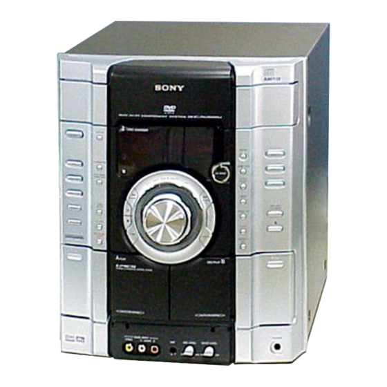
(Photo: HCD-RV888D)
Model Name Using Similar Mechanism
DVD
DVD Mechanism Type
Section
Optical Pick-up Name
Tape Deck Model Name Using Similar Machanism
Section
Tape Transport Mechanism Type
SPECIFICATIONS
Inputs
VIDEO/SAT IN (audio) (phono jacks):
GAME INPUT VIDEO (phono jack):
GAME INPUT AUDIO (phono jacks):
MIC (phone jack):
Outputs
VIDEO/SAT OUT (audio) (phono jacks):
VIDEO OUT (phono jack):
S-VIDEO OUT (4-pin/mini-DIN jack):
COMPONENT VIDEO OUT:
E Model
Australian Model
NEW
CDM74S-DVBU62
DBU-3
HCD-RV660D/RV990D
CWM43RR-35
voltage 450/250 mV,
impedance 47 kilohms
1 Vp-p, 75 ohms
voltage 250 mV,
impedance 47 kilohms
sensitivity 1 mV,
impedance 10 kilohms
voltage 250 mV,
impedance 1 kilohm
max. output level
1 Vp-p, unbalanced, Sync
negative, load impedance
75 ohms
Y: 1 Vp-p, unbalanced,
Sync negative,
C: 0.286 Vp-p, load
impedance 75 ohms
Y: 1 Vp-p, 75 ohms
P
, P
: 0.7 Vp-p, 75 ohms
B
R
– Continued on next page –
DVD DECK RECEIVER
1
Advertisement
Table of Contents

Related Manuals for Sony HCD-RV777D


Summary of Contents for Sony HCD-RV777D
- Page 1 The following measured at AC 120, 127, 220, 230 – 240 V, 50/60 Hz Continuous RMS power output (reference) 100 + 100 watts DVD DECK RECEIVER (6 ohms at 1 kHz, 10% THD) Sony Corporation 9-877-866-01 2004F04-1 Home Audio Company © 2004. 06 Published by Sony Engineering Corporation...
- Page 2 COMPONENTS IDENTIFIED BY MARK 0 OR DOTTED LINE WITH MARK 0 ON THE SCHEMATIC DIAGRAMS AND IN THE PARTS LIST ARE CRITICAL TO SAFE OPERATION. REPLACE THESE COMPONENTS WITH SONY PARTS WHOSE PART NUMBERS APPEAR AS SHOWN IN THIS MANUAL OR IN SUPPLEMENTS PUBLISHED BY SONY.
- Page 3 HCD-RV777D/RV888D/RV999D Notes on Chip Component Replacement NOTES ON LASER DIODE EMISSION CHECK • Never reuse a disconnected chip component. The laser beam on this model is concentrated so as to be focused on • Notice that the minus side of a tantalum capacitor may be the disc reflective surface by the objective lens in the optical pick- damaged by heat.
- Page 4 HCD-RV777D/RV888D/RV999D MODEL IDENTIFICATION – BACK PANEL – PARTS No. MODEL PARTS No. RV999D: E3, E15 4-254-657-0s RV999D: EA 4-254-657-1s RV999D: MY, SP 4-254-657-2s RV999D: AUS 4-254-657-3s RV999D: PH 4-254-657-5s RV999D: MX 4-254-657-6s RV999D: E51 4-254-657-7s RV999D: AR 4-254-657-9s RV888D: E3, E15...
-
Page 5: Table Of Contents
7-26. Schematic Diagram –Video Section– ........ 71 3-8. Main Board (HCD-RV888D/RV999D) ......17 7-27. Printed Wiring Board –Front AMP Section– ....72 3-9. Main Board (HCD-RV777D) ..........17 7-28. Schematic Diagram –Front AMP Section– ....... 73 3-10. Surround Amp Board, Front Amp Board 7-29. -
Page 6: Service Note
HCD-RV777D/RV888D/RV999D SECTION 1 SERVICE NOTE 1-1. SERVICE POSITION OF CDM RF board DVD mechanism block J-2501-103-A stand... -
Page 7: Service Position Of Dmb07 Board, Video Board
HCD-RV777D/RV888D/RV999D 1-2. SERVICE POSITION OF DMB07 BOARD, VIDEO BOARD VIDEO board DMB07 board Note : Remove the board and then reassemble the CD block. J-2501-103-A VIDEO board DMB07 board stand VIDEO board DMB07 board... -
Page 8: Service Position Of Tcm
HCD-RV777D/RV888D/RV999D 1-3. SERVICE POSITION OF TCM tape mechanism 1-4. SERVICE POSITION OF FRONT AMP BOARD insulating plate FRONT AMP board HP board Note1: For sounding, remove the HP board from the front panel and connect it. Note2: Connect the ground (3 places) -
Page 9: Note Of Transformer
HCD-RV777D/RV888D/RV999D 1-5. NOTE OF TRANSFORMER power cord transformer Pull the power cord in the direction of the arrow A (T901) with care to keep the cord from contact with the transformer (T901). SUB TRANS board more than 3mm Then fix the cord using two clips indicated by the arrow B . -
Page 10: General
HCD-RV777D/RV888D/RV999D SECTION 2 GENERAL This section is extracted from instruction manual. - Page 11 HCD-RV777D/RV888D/RV999D...
-
Page 12: Disassembly
(Page 16) VIDEO BOARD (Page 18) 3-8. MAIN BOARD (HCD-RV888D/RV999D) (Page 17) 3-12. RF BOARD, PICK-UP UNIT 3-9. MAIN BOARD (HCD-RV777D) (Page 19) (Page 17) 3-13. SW BOARD, 3-10. SURROUND AMP BOARD, DRIVER BOARD FRONT AMP BOARD (Page 19) (HCD-RV888D/RV999D) (Page 18) 3-14. - Page 13 HCD-RV777D/RV888D/RV999D Note : Follow the disassembly procedure in the numerical order given. 3-1. CASE 5 four screws (+BVTT 3 × 6) 9 case 4 screw (case 3 TP2) 2 screw (case 3 TP2) 3 two screws (case 3 TP2) 6 three screws (+BVTT 3 ×...
- Page 14 HCD-RV777D/RV888D/RV999D 3-3. FRONT PANEL SECTION, DVD BLOCK SECTION 5 screw 2 screw (+BVTP 3 × 8) (+BVTT 3 × 6) two lugs 8 CN706 3 screw (+BVTT 3 × 6) 4 screw (+BVTP 3 × 8) 7 CN503 9 CN605 0 connector 1 three screws (+BVTT 3 ×...
-
Page 15: Panel Board
HCD-RV777D/RV888D/RV999D 3-4. TAPE MECHANISM DECK 1 two screws (+BVTP 2.6 × 8) 2 three screws (+BVTP 2.6 × 8) 3 two screws (+BVTP 2.6 × 8) 4 tape mechanism deck 3-5. PANEL BOARD 3 seven claws 1 eight screws 4 CN2 (+BVTP 2.6 ×... -
Page 16: Jack Board
HCD-RV777D/RV888D/RV999D 3-6. JACK BOARD 1 two screws (+BVTP 2.6 × 8) 4 shield plate 6 JACK board 3 screw 2 screw (+BVTP 2.6 × 8) (+BVTP 2.6 × 8) 5 two mic knobs 3-7. BACK PANEL SECTION 2 CN901 qs back panel section 9 two screws (+BVTT 3 ×... -
Page 17: Main Board (Hcd-Rv888D/Rv999D)
5 screw (+BVTT 3 × 6) CN705 1 screw CN707 (+BVTT 3 × 6) 4 CN913 3-9. MAIN BOARD (HCD-RV777D) 9 screw 8 two screws (+BVTT 3 × 6) (+BVTP 3 × 6) 7 screw (+BVTT 3 × 6) claw... -
Page 18: Surround Amp Board, Front Amp Board
HCD-RV777D/RV888D/RV999D 3-10. SURROUND AMP BOARD, FRONT AMP BOARD (HCD-RV888D/RV999D) 5 SURROUND AMP board 2 CN372 4 two screws (+BVTP 3 × 8 ) 6 FRONT AMP board 1 CN302 3 two screws (+BVTP 3 × 16) 3-11. DVD MECHANISM BLOCK, DMB07 BOARD, VIDEO BOARD... -
Page 19: Rf Board, Pick-Up Unit
HCD-RV777D/RV888D/RV999D 3-12. RF BOARD, PICK-UP UNIT 8 step screw (M) 6 step screw (M) 0 insulator qa insulator(RB) 7 step screw (M) qs pick-up unit 9 insulator holder (DBU) assy 1 floating screw (+PTPWH M2.6) 5 RF board 4 CN001... -
Page 20: Sensor Board
HCD-RV777D/RV888D/RV999D 3-14. SENSOR BOARD 1 floating screw (+PTPWH M2.6) 2 tray 8 screw (+BTTP (M2.6)) 3 belt (table) 9 SENSOR board 4 floating screw (+PTPWH M2.6) 5 pulley (table) 6 floating screw (+PTPWH M2.6) 0 CN731 7 gear (geneva) 3-15. MOTOR (TB) BOARD... -
Page 21: Motor (Ld) Board
HCD-RV777D/RV888D/RV999D 3-16. MOTOR (LD) BOARD 2 two screws (+BTTP (M2.6)) 4 Remove the two solderings of motor. 3 MOTOR (LD) board 5 loading motor assy (M751) 1 belt (loading) -
Page 22: Test Mode
HCD-RV777D/RV888D/RV999D SECTION 4 TEST MODE [Cold Reset] [GC Test Mode] • The cold reset clears all data including preset data stored in the • This mode is used to check the fluorescent indicator tube, LEDs, RAM to initial conditions. Execute this mode when returning keyboard, volume and phones. - Page 23 HCD-RV777D/RV888D/RV999D [MC Test Mode] [Aging Mode] • This mode is used to check operations of the respective sections This mode can for operation check of tape deck section. of Amplifier, Tuner, and Tape. • If an error occurred: Procedure: The aging operation stops and display then status.
- Page 24 HCD-RV777D/RV888D/RV999D [DVD Service Mode] 2. CDM Error History <CDM74S Error History Display> • The sequence during the aging mode is following as below. 11 digits are displayed after the M character. Aging mode sequence (DVD section): Example of display : M0FF400220000...
- Page 25 HCD-RV777D/RV888D/RV999D [REPEAT 5 LIMIT OFF MODE] DVD OSD Test Mode • This mode is used to enable infinite repetitions. Normally, the number of repetitions allowed is 5. [GENERAL DESCRIPTION] Procedure: The Test Mode allows you to make diagnosis and adjustment easily 1.
- Page 26 HCD-RV777D/RV888D/RV999D 0-1. All (All items continuous check) 0-2-4. Model Type This menu checks all diagnostic items continuously. Normally, all Model name is displayed. (MHC-RVXXXD) items are checked successively one after another automatically unless an error is found, but at a certain item that requires judgment 0-2-5.
- Page 27 HCD-RV777D/RV888D/RV999D Note: During adjustment of each disc, the measurement for disc 1-3. DVD-DL (dual layers) type judgment is made. As automatic adjustment does not Press the 3 button on the remote commander and insert a DVD judge the disc type unlike conventional models, take care dual layers disc following the message.
- Page 28 HCD-RV777D/RV888D/RV999D In using the manual operation menu, take care of the following Mirr Time : Mirror time of between disc surface and record points. These commands do not provide protection, thus requiring surface when disc type judgment. (hexadecimal correct operation. The sector address or time code field is displayed number) when a disc is loaded.
- Page 29 HCD-RV777D/RV888D/RV999D when CLVA is turned on, the usual trace mode becomes active. In for the selected item will be displayed, then increase or decrease the trace mode, DVD sector address or CD time code is displayed. numeric value with the O button or o button. If CLV has been This is not displayed where the spindle is not locked.
- Page 30 HCD-RV777D/RV888D/RV999D 2-9. SACD Water Mark Check (Not used) EEPROM Data 2/2 CDRW DVDRW Focus Gain SACD Water Mark Check Trk. Gain Focus Offset Trk. Offset Boost PSP AMP Prev:UP Default:CLR Exit:RET Start: ENTER Stop: RETURN On this screen, current servo adjusted data stored in the EEPROM are displayed.
- Page 31 HCD-RV777D/RV888D/RV999D xxxxhxxm : The laser on total hours. Data below minutes are aa: Initialization is completed or not. omitted. : Complete. : Error number. other number : Not complete. : Error code. bb: Operating status of mechanism deck at an error occurred.
- Page 32 HCD-RV777D/RV888D/RV999D 6. VERSION INFORMATION On the Test Mode Menu screen, selecting 6 displays the ROM version and region code. The parenthesized hexadecimal number in version field is checksum value of ROM. ## Version Information ## IF con. Ver.x. xx SYScon.
-
Page 33: Mechanical Adjustments
HCD-RV777D/RV888D/RV999D SECTION 5 MECHANICAL ADJUSTMENTS Precaution 1. Clean the following parts with a denatured alcohol-moistened swab: record/playback heads pinch rollers erase head rubber belts capstan idlers 2. Demagnetize the record/playback head with a head demagnetizer. 3. Do not use a magnetized screwdriver for the adjustments. -
Page 34: Electrical Adjustments
HCD-RV777D/RV888D/RV999D SECTION 6 ELECTRICAL ADJUSTMENTS DVD SECTION DECK SECTION 0 dB=0.775 V About the dicision to pass or fail of the optical pick-up block, refer 1. Demagnetize the record/playback head with a head to “DICISION TO PASS OR FAIL OF THE OPTICAL PICK-UP demagnetizer. - Page 35 HCD-RV777D/RV888D/RV999D 2. Turn the adjustment screw and check output peaks. If the peaks Adjustment Location: Playback Head (Deck A). do not match for L-CH and R-CH, turn the adjustment screw Record/Playback/Erase Head (Deck B). so that outputs match within 1dB of peak.
-
Page 36: Diagrams
HCD-RV777D/RV888D/RV999D SECTION 7 DIAGRAMS 7-1. IC PIN DESCRIPTIONS • IC701 TMC57929PGF-RDP (DVD DECODER) (DMB07 Board (3/8)) Pin No. Pin Name Pin Description 1, 2 D5, D6 Two-way data bus signal input from/output to mechanism control IC. — Ground pin Two-way data bus signal input from/output to mechanism control IC. - Page 37 HCD-RV777D/RV888D/RV999D Pin No. Pin Name Pin Description 59, 60 HA0, HA2 Not used in this set. (Fixed at H.) — Ground pin 62, 63 HCS0, HCS1 Not used in this set. (Open) — Power supply pin (+3.2 V) DASP Not used in this set. (Fixed at H.)
- Page 38 HCD-RV777D/RV888D/RV999D Pin No. Pin Name Pin Description Spindle motor control signal output to focus/tracking coil driver, spindle/sled motor driver IC. Middle point voltage (+1.65 V) input MDIN2 Spindle motor servo drive signal input MDIN1 MDP input VCCA1 — Power supply pin (+3.2 V) CLVS Control signal output to selection the spindle control filter constant at CLVS.
- Page 39 HCD-RV777D/RV888D/RV999D • IC901 CXP973064-243R (MECHANISM CONTROL) (DMB07 Board (5/8)) Pin No. Pin Name Pin Description NO_USE Not used. (Open) Serial data enable signal output to CD/DVD/SACD RF amp, focus/tracking error amp SDEN DOCTRL/ISBTEST Digital out ON/OFF control signal output to CD decoder, digital servo processor IC.
- Page 40 HCD-RV777D/RV888D/RV999D Pin No. Pin Name Pin Description 56, 57 CONTROL_2, CONTROL_1 Not used. GFS_DVD Guard frame sync signal input from DVD decoder IC. MUTE_CD Muting ON/OFF control signal output to CD decoder, digital servo processor IC. Muting ON/OFF control signal output to focus/tracking coil driver, spindle/sled motor MUTE_2D driver IC.
- Page 41 HCD-RV777D/RV888D/RV999D • IC207 ZIVA5X-C2F (DVD SYSTEM PROCESSOR) (DMB07 Board (7/8)) Pin No. Pin Name Pin Description VDDP — Power supply pin (+3.2 V) (I/O signal) Address bus signal input from/output to bus interface IC. 3 to 11 HAD15 to HAD7 Data bus (address signal multiplexed) signal input from/output to bus interface IC.
- Page 42 Serial data output to 2CH DAC IC (HCD-RV777D) and D/A converter IC (HCD- RV888D/RV999D). Serial data clock signal output to 2CH DAC IC (HCD-RV777D) and D/A converter IC (HCD-RV888D/RV999D). Latch enable signal output to 2CH DAC IC (HCD-RV777D) and D/A converter IC (HCD-RV888D/RV999D).
- Page 43 HCD-RV777D/RV888D/RV999D Pin No. Pin Name Pin Description Audio data (front L/R signal) output to 2CH DAC IC (HCD-RV777D) and D/A DATA1(FLR) converter IC (HCD-RV888D/RV999D). VDDP — Power supply pin (+3.2 V) (I/O signal) GNDP — Ground pin (I/O signal) DATA2(SLR) Audio data (rear L/R signal) output to D/A converter IC (HCD-RV888D/RV999D).
- Page 44 HCD-RV777D/RV888D/RV999D • IC701 M30620MCN-A38FPU0 (MASTER CONTROL) (MAIN Board (3/3)) Pin No. Pin Name Pin Description S-OUT Serial out signal output S-CLK Serial clock signal output M61530-CLK M61530FP clock signal output SIRCS Sircs signal input M61530-DATA M61530FP data signal output M61530-DATA...
- Page 45 HCD-RV777D/RV888D/RV999D Pin No. Pin Name Pin Description HP-SW Headphones in/out select signal input (L: out, H: in) MIC-SW Microphone in/out select signal input (L: out, H: in) A-TRG Trigger out ON/OFF select signal output (deck A) (L: OFF, H: ON)
- Page 46 HCD-RV777D/RV888D/RV999D • IC101 µPD780232GC-504-8BT-A (SYSTEM CONTROL) (PANEL Board) Pin No. Pin Name Pin Description — Power supply pin (+3.3 V) — Ground pin System clock signal input (5 MHz) System clock signal input (5 MHz) Directly connect to ground. RESET...
-
Page 47: Block Diagram -Dvd Dsp Section
HCD-RV777D/RV888D/RV999D 7-2. BLOCK DIAGRAM — DVD DSP SECTION — CD/DVD/SACD RF AMP, DVD DECODER DVD SYSTEM PROCESSOR OPTICAL PICK-UP FOCUS/TRACKING ERROR AMP IC701 IC207 BLOCK IC001 CD DECODER, DIGITAL SERVO PROCESSOR 63 RFSIN IC509 44,41,39,35 177-174, SDDATA0-SDDATA7 HDB0-HDB7 DVDRFP IEC958... -
Page 48: Block Diagram -Dac Section
HCD-RV777D/RV888D/RV999D 7-3. BLOCK DIAGRAM — DAC SECTION — RV777D RV777D IC303 OPTICAL OUT SELECTOR IC252 ICE958 DIGITAL OPTICAL J102 TRANSMITTER DIGITAL OUT SUB WOOFER IC302 (OPTICAL) RV888D/RV999D RV888D/RV999D SURROUND CONTROL POWER AMP D/A CONVERTER CDSEL TM401 IC301 IC301 IC302 DATA0... -
Page 49: Block Diagram -Main Section
HCD-RV777D/RV888D/RV999D 7-4. BLOCK DIAGRAM — MAIN SECTION — REC/PB AMP, SOUND CONTROLLER TM901 IC101 FM 75Ω FRONT PB MUTE SUR1 COAXIAL DOWN MIX Q111,607,608 SECTION (Page 48) R-CH TUNER INB1 TONE A+9V TONE OVERLOAD DET SECTION PB(DECK A) MUTE PB A... -
Page 50: Block Diagram -Dvd Sys Section
HCD-RV777D/RV888D/RV999D 7-5. BLOCK DIAGRAM — DVD SYS SECTION — DISPLAY CONTROL MASTER CONTROL IC101 IC701 (3/3) IC392 S13-22 AU+3.3V FUNCTION AU+3.3V AU+5V 22 KEY0 DISPLAY STANDBY DISPLAY KEY D192 S31-40 I / I IC211 I / I POWER KEY FUNCTION KEY1 D+1.8V... -
Page 51: Circuit Boards Location
HCD-RV777D/RV888D/RV999D 7-6. CIRCUIT BOARDS LOCATION 7-7. NOTE FOR PRINTED WIRING BOARDS AND SCHEMATIC DIAGRAMS Note on Printed Wiring Board: Note on Schematic Diagram: • X : parts extracted from the component side. • All capacitors are in µF unless otherwise noted. (p: pF) SUB TRANS board •... -
Page 52: Schematic Diagram -Dvd Mechanism Section (1/2)
HCD-RV777D/RV888D/RV999D 7-9. SCHEMATIC DIAGRAM — DVD MECHANISM SECTION (1/2) — • Refer to page 84 for IC Block Diagram. R026 C006 C028 C027 C013 C031 CN002 C030 C026 C025 R023 C029 C024 C035 JL005 R024 JL004 CN001 R025 JL007 C009... - Page 53 HCD-RV777D/RV888D/RV999D 7-11. SCHEMATIC DIAGRAM — DVD MECHANISM SECTION (2/2) — • Refer to page 84 for IC Block Diagrams. IC701 IC B/D R702 R701 D701 C715 CN704 C751 CN721 M751 IC712 IC B/D R712 R713 CN705 C752 CN751 S751 D711...
- Page 54 HCD-RV777D/RV888D/RV999D 7-13. SCHEMATIC DIAGRAM — DMB07 SECTION (1/8) — • Refer to page 84 for IC Block Diagrams. (Page 63) (Page 61) CN107 R310 CL309 R311 R312 CL310 (Page 64) CL311 D392 FL302 CL312 R313 (Page C324 IC392 CL313 61, 63, 64)
- Page 55 HCD-RV777D/RV888D/RV999D 7-14. SCHEMATIC DIAGRAM — DMB07 SECTION (2/8) — • Refer to page 84 for IC Block Diagram. FL502 CL501 C522 C567 C568 R537 L501 R536 R545 R548 CN501 CL544 CL537 IC503 C507 R694 CL536 C592 R555 R591 CL535 C516...
-
Page 56: Schematic Diagram -Dmb07 Section (1/8)
HCD-RV777D/RV888D/RV999D 7-15. SCHEMATIC DIAGRAM — DMB07 SECTION (3/8) — C701 R786 C705 C733 R787 R700 C782 FL701 R788 FL706 C703 C715 C783 R789 C702 C729 C708 C709 C712 R710 C711 C716 C717 IC703(2/2) R707 R712 R709 C706 R708 R711 R725... -
Page 57: Schematic Diagram -Dmb07 Section (2/8)
HCD-RV777D/RV888D/RV999D 7-16. SCHEMATIC DIAGRAM — DMB07 SECTION (4/8) — • Waveforms – DMB07 Board – 1V/DIV, 20ns/DIV (Page 59) 3.9Vp-p 50ns IC901 (XTAL) 1V/DIV, 10ns/DIV 5.6Vp-p 37ns IC906 (MO1) 1V/DIV, 10ns/DIV C526 C527 4.5Vp-p (Page 62) R589 R580 R581 37ns... -
Page 58: Schematic Diagram -Dmb07 Section (5/8)
HCD-RV777D/RV888D/RV999D • Refer to page 61 for Waveforms. 7-17. SCHEMATIC DIAGRAM — DMB07 SECTION (5/8) — • Refer to page 85 for IC Block Diagrams. (Page 60) FL901 IC902 R901 C902 C901 Q901 (Page 61) IC904 IC903 IC B/D CL922... -
Page 59: Schematic Diagram -Dmb07 Section (6/8)
HCD-RV777D/RV888D/RV999D 7-18. SCHEMATIC DIAGRAM — DMB07 SECTION (6/8) — • Refer to page 86 for IC Block Diagram. (Page 60) (Page 64) (Page 62) CN202 (Page 58) R270 RB202 CN105 R288 R1001 IC B/D RB203 IC252 R9998 R9999 C289 R239... -
Page 60: Schematic Diagram -Dmb07 Section (7/8)
HCD-RV777D/RV888D/RV999D • Refer to page 61 for Waveforms. 7-19. SCHEMATIC DIAGRAM — DMB07 SECTION (7/8) — • Refer to page 86 for IC Block Diagram. (Page 63) R263 R264 R265 R266 R267 R222 R221 R290 (Page 58) R251 C226 C276... - Page 61 HCD-RV777D/RV888D/RV999D 7-20. SCHEMATIC DIAGRAM — DMB07 SECTION (8/8) — IC203 C218 C220 C255 FL203 C258 C259 C227 FL204 C205 C235 IC206 C239 C240 R301 C201 (Page 64) C264 R250 R215 C243 C245 C202 C246 C249 C254 C250 C203 C275 (Page 64)
-
Page 62: Schematic Diagram -Main Section (1/3)
HCD-RV777D/RV888D/RV999D 7-22. SCHEMATIC DIAGRAM — MAIN SECTION (1/3) — R376 C335 R176 J102 C271 R271 R381 Q377 R177 C172 C371 R377 R382 R397 R386 R727 Q705 C201 Q703 R729 Q704 R144 Q142 R146 IC302 C272 R372 R387 R145 C142 FB561... -
Page 63: Schematic Diagram -Main Section (2/3)
HCD-RV777D/RV888D/RV999D 7-23. SCHEMATIC DIAGRAM — MAIN SECTION (2/3) — (Page 67) R131 JR601 LP801 JR602 LP802 LP803 JR603 LP804 R130 R152 R658 R656 LP805 C161 C658 C163 R157 Q151 CN602 Q152 C611 C612 R611 R158 R156 JR104 C651 C652 R651... -
Page 64: Schematic Diagram -Main Section (3/3)
HCD-RV777D/RV888D/RV999D 7-24. SCHEMATIC DIAGRAM — MAIN SECTION (3/3) — • Refer to page 67 for Waveforms. (Page 67) R974 R973 R972 R862 C821 R858 R861 C815 C814 FB862 R863 R859 R860 D735 R755 NO708 C739 C791 R753 R754 C862 D734... -
Page 65: Schematic Diagram -Video Section
HCD-RV777D/RV888D/RV999D 7-26. SCHEMATIC DIAGRAM — VIDEO SECTION — • Refer to page 86 for IC Block Diagram. IC803 Q851 CN805 C851 C852 Q852 NO803 JW858 (Page 62) CN804 R850 C876 C877 R851 IC804 (Page 61) Q857 Q853 (Page 67) L862... -
Page 66: Schematic Diagram -Front Amp Section
HCD-RV777D/RV888D/RV999D 7-28. SCHEMATIC DIAGRAM — FRONT AMP SECTION — IC201 IC932 R216 NO272 R217 (Page 75) C934 C933 R218 Q216 Q217 IC934 R214 D271 R215 R213 C938 C937 NO271 C271 C273 R271 CN206 TH201 IC923 C203 (Page 81) C272 C274... -
Page 67: Schematic Diagram -Surround Amp Section
HCD-RV777D/RV888D/RV999D 7-30. SCHEMATIC DIAGRAM — SURROUND AMP SECTION (HCD-RV888D/RV999D) — (Page 73) IC301 R318 R317 CN302 R316 Q316 R314 D371 Q317 R315 C371 NO371 C373 R373 TH301 C372 (Page 81) C374 R374 R381 R305 RY381 R301 L381 C301 C303 R307... -
Page 68: Schematic Diagram -Panel Section
HCD-RV777D/RV888D/RV999D 7-32. SCHEMATIC DIAGRAM — PANEL SECTION — • Refer to page 76 for Waveform. C205 CN103 IC202 C206 R206 CN113 FB102 CN101 C207 C208 FB101 C121 R205 D192 C101 C160 (Page 69) C102 C161 R105 X101 R106 R107 C106... -
Page 69: Schematic Diagram -Jack Section
HCD-RV777D/RV888D/RV999D 7-34. SCHEMATIC DIAGRAM — JACK SECTION — C517 IC501(2/2) C510 IC501(1/2) R513 C515 C514 C512 R507 J503 C519 C518 R512 R514 R511 R510 C516 RV501 C511 R506 R516 R509 R508 R517 C513 D505 NO502 R515 C509 C520 C521 R518... -
Page 70: Schematic Diagram -Trans Section
HCD-RV777D/RV888D/RV999D 7-36. SCHEMATIC DIAGRAM — TRANS SECTION — F916 CN913 FH922 FH921 (Page 75) F914 T911 NO911 FH918 FH917 CN915 JW972 JW923 (Page 83) FH924 FH923 (Page 73) F917 FH920 FH919 F915 F918 FH926 FH925 CN914 FH928 FH927 F919 C915... -
Page 71: Schematic Diagram -Sub Trans Section
HCD-RV777D/RV888D/RV999D 7-38. SCHEMATIC DIAGRAM — SUB TRANS SECTION — (RV888D : AUS / RV999D : AUS,AR) F911 (RV888D : EXCET AUS / RV999D : EXCEPT AUS,AR) FH912 FH911 CN902 F912 FH914 FH913 FH916 FH915 F913 JW907 (Page 81) JW906 R904... -
Page 72: Ic Block Diagrams
HCD-RV777D/RV888D/RV999D 7-39. IC BLOCK DIAGRAMS IC701 BA6956AN (DRIVER Board) IC509 CXD3068Q (DMB07 Board) IC712 BA6956AN (DRIVER Board) IC001 SP3723CAFOPM (RF Board) 64 63 62 61 60 59 55 54 53 52 FAST ATTACK CONTROL LOGIC INPUT OUTPUT HOLD FULL WAVE... - Page 73 HCD-RV777D/RV888D/RV999D IC331 PCM1751DBQR (DMB07 Board) DATA LRCK DGND SYSTEM SYSTEM POWER CLOCK CLOCK SUPPLY MANAGER OUTPUT AMP SERIAL L OUT CONTROL LOW-PASS PORT 4x/8x FILTER ENHANCED OVERSAMPLING MULTI-LEVEL DIGITAL DELTA-SIGMA FILTER MODULATOR WITH FUNCTION AUDIO OUTPUT AMP CONTROLLER SERIAL R OUT...
- Page 74 HCD-RV777D/RV888D/RV999D IC204 BR9040F-WE2 (DMB07 Board) 8 WC DETECT SUPPLY INSTRUCTION DECODE VOLTAGE CONTROL AND CLOCK GENERATOR HIGH WRITE VOLTAGE DISABLE GENERATOR ADDRESS ADDRESS 8bit DECODER INSTRUCTION BUFFER 8bit 4,096bit REGISTER EEPROM DATA 16bit AMPS REGISTER 16bit IC252 TC7WH157FK (TE85R) (DMB07 Board)
-
Page 75: Exploded Views
HCD-RV777D/RV888D/RV999D SECTION 8 EXPLODED VIEWS NOTE: • The mechanical parts with no reference • Abbreviation The components identified by mark 0 or dotted line with mark number in the exploded views are not supplied. E3 : 240 V AC area in E model 0 are critical for safety. -
Page 76: Front Panel Section (1)
HCD-RV777D/RV888D/RV999D 8-2. FRONT PANEL SECTION (1) not supplied (SIRCS board) FL1001 not supplied not supplied not supplied MX model not supplied (HP board) not supplied Ref. No. Part No. Description Remark Ref. No. Part No. Description Remark 4-951-620-01 SCREW (2.6X8), +BVTP... -
Page 77: Front Panel Section (2)
HCD-RV777D/RV888D/RV999D 8-3. FRONT PANEL SECTION (2) not supplied not supplied Ref. No. Part No. Description Remark Ref. No. Part No. Description Remark 4-231-841-01 SPRING (HEART CAM-B) 4-231-836-01 SPRING (HEART CAM-A) 4-231-825-01 CAM (B), HEART 4-252-218-11 BUTTON (VIDEO/SAT) 4-224-104-41 DAMPER 4-252-203-21 BUTTON (POWER) -
Page 78: Front Panel Section (3)
HCD-RV777D/RV888D/RV999D 8-4. FRONT PANEL SECTION (3) not supplied not supplied not supplied not supplied (P-STREAM board) not supplied not supplied not supplied Ref. No. Part No. Description Remark Ref. No. Part No. Description Remark 4-252-202-11 DOOR (B), CASS 4-252-200-01 COVER, BUTTON 4-252-201-11 DOOR (A), CASS 4-252-208-11 BUTTON (FR/ALBUM–) -
Page 79: Dvd Block Section
HCD-RV777D/RV888D/RV999D 8-5. DVD BLOCK SECTION CDM74S-DVBU62 not supplied not supplied not supplied supplied not supplied not supplied not supplied not supplied not supplied not supplied Ref. No. Part No. Description Remark Ref. No. Part No. Description Remark A-4751-861-A VIDEO BOARD, COMPLETE... -
Page 80: Main Board Section (1/2)
HCD-RV777D/RV888D/RV999D 8-6. MAIN BOARD SECTION (1/2) HCD-RV888D/RV999D not supplied IC301 F919 T911 IC201 not supplied not supplied F918 IC921 IC922 F915 IC923 IC934 F914 IC932 not supplied F916 (LEAD PIN board) F917 not supplied HCD-RV777D not supplied not supplied not supplied... -
Page 81: Main Board Section (2/2)
HCD-RV777D/RV888D/RV999D 8-7. MAIN BOARD SECTION (2/2) HCD-RV888D/RV999D not supplied IC301 F919 T911 IC201 not supplied not supplied F918 IC921 IC922 F915 IC923 IC934 F914 IC932 not supplied F916 (LEAD PIN board) F917 not supplied HCD-RV777D not supplied not supplied not supplied... -
Page 82: Dvd Mechanism Deck Section (1)
HCD-RV777D/RV888D/RV999D 8-8. DVD MECHANISM DECK SECTION (1) (CDM74S-DVBU62) M741 chassis assy Ref. No. Part No. Description Remark Ref. No. Part No. Description Remark 4-218-253-21 SCREW (M2.6), +BTTP 4-243-820-01 GEAR (TABLE) 1-776-182-11 WIRE (FLAT TYPE) (5 CORE) 4-243-819-01 GEAR (GENEVA) 1-687-134-12 MOTOR (TB) BOARD... -
Page 83: Dvd Mechanism Deck Section (2)
HCD-RV777D/RV888D/RV999D 8-9. DVD MECHANISM DECK SECTION (2) (CDM74S-DVBU62) RE701 M751 The components identified by mark 0 or dotted line with mark 0 are critical for safety. Replace only with part number specified. Ref. No. Part No. Description Remark Ref. No. -
Page 84: Electrical Parts List
HCD-RV777D/RV888D/RV999D SECTION 9 DMB07 ELECTRICAL PARTS LIST NOTE: • Due to standardization, replacements in • SEMICONDUCTORS When indicating parts by reference the parts list may be different from the In each case, u : µ, for example: number, please include the board. - Page 85 HCD-RV777D/RV888D/RV999D DMB07 Ref. No. Part No. Description Remark Ref. No. Part No. Description Remark C308 1-164-874-11 CERAMIC CHIP 100PF C544 1-125-777-11 CERAMIC CHIP 0.1uF C309 1-164-874-11 CERAMIC CHIP 100PF C545 1-117-370-11 CERAMIC CHIP 10uF C321 1-126-206-11 ELECT CHIP 100uF 6.3V...
- Page 86 HCD-RV777D/RV888D/RV999D DMB07 Ref. No. Part No. Description Remark Ref. No. Part No. Description Remark C760 1-164-943-11 CERAMIC CHIP 0.01uF < DIODE > C761 1-164-943-11 CERAMIC CHIP 0.01uF C762 1-164-943-11 CERAMIC CHIP 0.01uF D202 8-719-988-61 DIODE 1SS355TE-17 C763 1-164-943-11 CERAMIC CHIP 0.01uF...
- Page 87 HCD-RV777D/RV888D/RV999D DMB07 Ref. No. Part No. Description Remark Ref. No. Part No. Description Remark IC903 6-704-004-01 IC BR24L16F-WE2 R257 1-216-829-11 METAL CHIP 4.7K 1/10W IC904 6-704-753-01 IC SN74AHC2G74HDCUR R259 1-216-829-11 METAL CHIP 4.7K 1/10W IC906 6-700-407-01 IC SM8707GV-G-E2 R260 1-216-829-11 METAL CHIP 4.7K...
- Page 88 HCD-RV777D/RV888D/RV999D DMB07 Ref. No. Part No. Description Remark Ref. No. Part No. Description Remark R504 1-216-841-11 METAL CHIP 1/10W R599 1-216-821-11 METAL CHIP 1/10W R505 1-216-841-11 METAL CHIP 1/10W R601 1-216-864-11 SHORT CHIP R506 1-216-841-11 METAL CHIP 1/10W R694 1-216-833-11 METAL CHIP...
- Page 89 HCD-RV777D/RV888D/RV999D DMB07 DRIVER Ref. No. Part No. Description Remark Ref. No. Part No. Description Remark R787 1-216-845-11 METAL CHIP 100K 1/10W R9998 1-216-864-11 SHORT CHIP R788 1-216-845-11 METAL CHIP 100K 1/10W R9999 1-216-864-11 SHORT CHIP R789 1-216-845-11 METAL CHIP 100K...
- Page 90 HCD-RV777D/RV888D/RV999D FRONT AMP Ref. No. Part No. Description Remark Ref. No. Part No. Description Remark A-1053-978-A FRONT AMP BOARD, COMPLETE (RV888D) D281 8-719-991-33 DIODE 1SS133T-77 A-4751-854-A FRONT AMP BOARD, COMPLETE (RV999D) D291 8-719-991-33 DIODE 1SS133T-77 A-4751-856-A FRONT AMP BOARD, COMPLETE (RV777D) <...
- Page 91 HCD-RV777D/RV888D/RV999D FRONT AMP JACK Ref. No. Part No. Description Remark Ref. No. Part No. Description Remark 0 R255 1-245-235-21 METAL 0.22 A-1053-972-A JACK BOARD, COMPLETE (RV999D:E51,AR,MX) 0 R256 1-245-235-21 METAL 0.22 A-4751-845-A JACK BOARD, COMPLETE R257 1-247-831-11 CARBON 1/4W (EXCEPT RV999D:E51,AR,MX)
- Page 92 HCD-RV777D/RV888D/RV999D JACK MAIN Ref. No. Part No. Description Remark Ref. No. Part No. Description Remark D507 8-719-988-61 DIODE 1SS355TE-17 R528 1-216-835-11 METAL CHIP 1/10W D508 8-719-988-61 DIODE 1SS355TE-17 (EXCEPT RV999D:E51,AR,MX) D1201 8-719-069-54 DIODE UDZSTE-175.1B R529 1-216-835-11 METAL CHIP 1/10W (EXCEPT RV999D:E51,AR,MX) (EXCEPT RV999D:E51,AR,MX) <...
- Page 93 HCD-RV777D/RV888D/RV999D MAIN Ref. No. Part No. Description Remark Ref. No. Part No. Description Remark C145 1-110-518-11 ELECT 10uF 100V C314 1-115-467-11 CERAMIC CHIP 0.22uF C151 1-126-964-11 ELECT 10uF (RV888D/RV999D) C152 1-126-961-11 ELECT 2.2uF C320 1-126-964-11 ELECT 10uF C153 1-126-961-11 ELECT 2.2uF...
- Page 94 HCD-RV777D/RV888D/RV999D MAIN Ref. No. Part No. Description Remark Ref. No. Part No. Description Remark C368 1-126-964-11 ELECT 10uF C772 1-107-696-11 ELECT 47uF (RV888D/RV999D) (RV888D/RV999D) C371 1-126-964-11 ELECT 10uF C773 1-107-696-11 ELECT 47uF C372 1-126-964-11 ELECT 10uF (RV888D/RV999D) (RV888D/RV999D) C774 1-107-696-11 ELECT...
- Page 95 HCD-RV777D/RV888D/RV999D MAIN Ref. No. Part No. Description Remark Ref. No. Part No. Description Remark D709 8-719-988-61 DIODE 1SS355TE-17 JR17 1-216-864-11 SHORT CHIP D710 8-719-988-61 DIODE 1SS355TE-17 JR104 1-216-837-11 METAL CHIP 1/10W D711 8-719-988-61 DIODE 1SS355TE-17 JR105 1-216-837-11 METAL CHIP 1/10W...
- Page 96 HCD-RV777D/RV888D/RV999D MAIN Ref. No. Part No. Description Remark Ref. No. Part No. Description Remark Q631 8-729-907-00 TRANSISTOR DTC114EU R155 1-216-821-11 METAL CHIP 1/10W Q661 8-729-029-10 TRANSISTOR DTC143TUA-T106 R156 1-216-841-11 METAL CHIP 1/10W Q662 8-729-905-35 TRANSISTOR 2SC4081-R R157 1-216-841-11 METAL CHIP...
- Page 97 HCD-RV777D/RV888D/RV999D MAIN Ref. No. Part No. Description Remark Ref. No. Part No. Description Remark R314 1-216-819-11 METAL CHIP 1/10W R383 1-216-845-11 METAL CHIP 100K 1/10W (RV888D/RV999D) (RV888D/RV999D) R320 1-216-833-11 METAL CHIP 1/10W R384 1-216-845-11 METAL CHIP 100K 1/10W (RV888D/RV999D) (RV888D/RV999D)
- Page 98 HCD-RV777D/RV888D/RV999D MAIN Ref. No. Part No. Description Remark Ref. No. Part No. Description Remark R665 1-216-829-11 METAL CHIP 4.7K 1/10W R779 1-216-821-11 METAL CHIP 1/10W R666 1-216-837-11 METAL CHIP 1/10W (RV888D/RV999D) R667 1-216-837-11 METAL CHIP 1/10W R780 1-216-833-11 METAL CHIP...
- Page 99 HCD-RV777D/RV888D/RV999D MAIN MOTOR (LD) MOTOR (TB) PANEL Ref. No. Part No. Description Remark Ref. No. Part No. Description Remark R875 1-216-809-11 METAL CHIP 1/10W A-4751-844-A PANEL BOARD, COMPLETE R885 1-216-809-11 METAL CHIP 1/10W ********************** R886 1-216-809-11 METAL CHIP 1/10W R887...
- Page 100 HCD-RV777D/RV888D/RV999D PANEL Ref. No. Part No. Description Remark Ref. No. Part No. Description Remark Q138 8-729-907-00 TRANSISTOR DTC114EU R138 1-216-813-11 METAL CHIP 1/10W Q139 8-729-907-00 TRANSISTOR DTC114EU R140 1-216-841-11 METAL CHIP 1/10W R141 1-216-841-11 METAL CHIP 1/10W < RESISTOR >...
- Page 101 HCD-RV777D/RV888D/RV999D PANEL P-STREAM Ref. No. Part No. Description Remark Ref. No. Part No. Description Remark 1-762-875-21 SWITCH, KEYBOARD C016 1-162-966-11 CERAMIC CHIP 0.0022uF 10% (PLAY MODE/TUNING MODE) C017 1-162-966-11 CERAMIC CHIP 0.0022uF 10% 1-762-875-21 SWITCH, KEYBOARD (GAME MIXING) C018 1-164-172-11 CERAMIC CHIP 0.0056uF 10%...
- Page 102 HCD-RV777D/RV888D/RV999D SENSOR SIRCS SUB TRANS SURROUND AMP Ref. No. Part No. Description Remark Ref. No. Part No. Description Remark R005 1-216-841-11 METAL CHIP 1/10W SUB TRANS BOARD R006 1-216-817-11 METAL CHIP 1/10W ***************** R007 1-216-803-11 METAL CHIP 1/10W R008 1-216-803-11 METAL CHIP...
- Page 103 HCD-RV777D/RV888D/RV999D SURROUND AMP Ref. No. Part No. Description Remark Ref. No. Part No. Description Remark C304 1-126-964-11 ELECT 10uF < DIODE > (RV888D/RV999D) C306 1-136-497-81 FILM 0.1uF D301 8-719-991-33 DIODE 1SS133T-77 (RV888D/RV999D) (RV888D/RV999D) D341 8-719-991-33 DIODE 1SS133T-77 (RV888D/RV999D) C307 1-136-497-81 FILM 0.1uF...
- Page 104 HCD-RV777D/RV888D/RV999D SURROUND AMP TRANS Ref. No. Part No. Description Remark Ref. No. Part No. Description Remark R316 1-247-879-11 CARBON 100K 1/4W R383 1-260-076-11 CARBON 1/2W F (RV888D/RV999D) (RV888D/RV999D) R317 1-247-879-11 CARBON 100K 1/4W R385 1-260-076-11 CARBON 1/2W F (RV888D/RV999D) (RV888D/RV999D)
- Page 105 HCD-RV777D/RV888D/RV999D TRANS VIDEO Ref. No. Part No. Description Remark Ref. No. Part No. Description Remark < CONNECTOR > C862 1-128-646-11 ELECT 1000uF 6.3V C863 1-117-317-11 ELECT 1000uF * CN913 1-564-518-11 PLUG, CONNECTOR 3P (RV888D/RV999D) C871 1-117-245-11 ELECT 330uF 6.3V * CN914...
- Page 106 HCD-RV777D/RV888D/RV999D VIDEO Ref. No. Part No. Description Remark Ref. No. Part No. Description Remark R827 1-247-804-11 CARBON 1/4W MISCELLANEOUS R831 1-249-429-11 CARBON 1/4W *************** R833 1-247-804-11 CARBON 1/4W R834 1-249-429-11 CARBON 1/4W 1-828-965-11 WIRE (FLAT TYPE) (11 CORE) R835 1-249-429-11 CARBON...
- Page 107 HCD-RV777D/RV888D/RV999D REVISION HISTORY Clicking the version allows you to jump to the revised page. Also, clicking the version at the upper on the revised page allows you to jump to the next revised page. Ver. Date Description of Revision 2004. 06...
Need help?
Do you have a question about the HCD-RV777D and is the answer not in the manual?
Questions and answers