Table of Contents
Advertisement
Quick Links
MITSUBISHI
Tape Format
: S-VHS/VHS NTSC standard with
Power Source
: 120 V AC ; 60 Hz
Power Consumption
: Approx. 28 W (standby 6.0 W)
Video Signal System
: EIA standard ; NTSC color
Video Recording System
: S-VHS standard/D-VHS standard
Luminance
: Frequency modulation recording
Color Signal
: Low frequency conversion
Hi-Fi Audio
: S-VHS standard
Recording System
Linear Audio Track
: 1 track
Maximum Recording Time
D-VHS
: 150 min. with DF-300 video cassette (HS)
S-VHS/VHS
: 120 min. with T-120 video cassette (SP)
Record/Playback System
Video
: 4 heads
Audio
: 2 Hi-Fi channels and 1 monoral audio control
Digital
: HS 4 heads
Rewind Time
: Approx. 43 seconds for T-120 cassette
MITSUBISHI DIGITAL ELECTRONICS AMERICA, INC.
9351 Jeronimo Ave. Irvine, California 92618 U.S.A.
Copyright C 2001 Mitsubishi Digital Electronics America, Inc. All Rights Reserved.
Only cassettes marked D-VHS or S-VHS or VHS can be used with this video cassette recorder.
SPECIFICATIONS
Hi-Fi audio and D-VHS standard
sub-carrier phase shift recording
Azimuth helical scanning system
300 min. with DF-300 video cassette (STD)
360 min. with T-120 video cassette (EP)
STD 2 heads
VIDEO CASSETTE RECORDER
Video Input
Audio Input
Video Output
Audio Output
Digital Interface
Input/Output
Tuner
VHF
UHF
CATV
Operating Temperature
Relative Humidity
RF Channel Output
Weight
Dimensions
Timer Program Capacity
Memory Backup Time
Deck
• Weight and dimensions shown are approximate.
• Design and specifications are subject to change without notice.
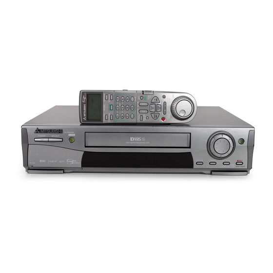
MODEL
HS-HD2000U
: 0.5 to 2.0 V(p-p), 75 Ω
unbalanced RCA pin Jack
: -346 mV(rms), 47 kΩ
unbalanced RCA pin Jack
: 1.0 V(p-p), 75 Ω unbalanced
RCA pin Jack
: -346 mV(rms), 1 kΩ unbalanced
RCA pin Jack
: based on IEEE 1394 digital
interface, 4 pin, corresponds to S400
: 54 to 88 MHz, 174 to 216 MHz
: 470 to 806 MHz
: 54 to 88 MHz, 90 to 804 MHz
: 41 °F to 104 °F
: 30 % to 80 %
: Channel 3 or 4 switchable
: Approx. 9.9 lbs (4.5 kg)
: 16.7"(W) × 3.7"(H) × 12.0"(D)
: 1 month programmable
/ 8 programs
: Approx. 30 minutes
: α Deck
2001
Advertisement
Table of Contents

Related Manuals for Mitsubishi HS-HD2000U


Summary of Contents for Mitsubishi HS-HD2000U
- Page 1 • Weight and dimensions shown are approximate. • Design and specifications are subject to change without notice. MITSUBISHI DIGITAL ELECTRONICS AMERICA, INC. 9351 Jeronimo Ave. Irvine, California 92618 U.S.A. Copyright C 2001 Mitsubishi Digital Electronics America, Inc. All Rights Reserved.
-
Page 2: Table Of Contents
CONTENTS – FILE “COVERPGE” – PULLEY GEAR ASSY, SLIP GEAR, SPECIFICATIONS ............1 SLIP SPRING, SLIP WASHER, CONTENTS..............2 THRUST WASHER, SLIP ADJUSTER, GLOSSARY OF ABBREVIATIONS ........4 IDLER UNIT ...........9 2-15 CAPSTAN BRAKE SPRING, – FILE “DISASSY” – CAPSTAN BRAKE ASSY ......11 SAFETY PRECAUTIONS ..........1 2-16 FC HOLDER, MOTOR HOLDER, CONNECTION ..............3... -
Page 3: Contents
CONTENTS TENSION POLE's Position ......30 Check and Adjustment of FM Envelope ..........31 3-2-1 GUIDE ROLLER Adjustment Check ....31 3-2-2 Height Adjustment of GUIDE ROLLER (SP) ........31 3-2-3 Height Adjustment of GUIDE ROLLER (TU) ........31 3-2-4 Coarse Adjustment of Phase .......32 3-2-5 Flatness Check of FM Waveform....32 3-2-6 Tape Running Condition at the GUIDE ROLLERs (Check1) ....33... -
Page 4: Glossary Of Abbreviations
GLOSSARY OF ABBREVIATIONS : Audio/Control JSTCLK : Just Clock A-PB : Audio Play Back A-REC : Audio Recording LIN-IN : Linear Audio In : Audio Erase LIN-OUT : Linear Audio Out AENV : Audio Envelope LMUTE : Linear Mute : Automatic Frequency Control : Long Play : Audio Flip Flop AFTV... -
Page 5: Safety Precautions
SAFETY PRECAUTIONS INTRODUCTION SAFETY NOTICE This manual provides service information for the adjustments Before returning VCR to the customer a safety check of the of mechanical and electrical operations. entire VCR should be made. The service technician must be Due to design modifications, the servicing procedures and sure that no protective device built into the instrument by the data given in this manual are subject to possible change manufacturer has become defective or inadvertently... - Page 6 2. Hot Check The test sequence, with reference to the measuring (2) Close switch S1, energizing the VCR, and immediately circuit in the figure is as follows: after closing the switch, measure leakage current using (1) With switch S1 open, connect the VCR to the measuring both positions of switch S2, and with the switching circuit.
-
Page 7: Connection
CONNECTION Connecting separate antennas (UHF/VHF) Now that you’ve completed the antenna connections to your Connecting the Television VCR, you’re ready to connect the VCR to the TV. To connect separate UHF/VHF antennas to the VCR: Because every television is different (especially older model 1. -
Page 8: Disassembly
DISASSEMBLY 1. Removal of Top Cover 1. Remove the two Top Cover fastening screws (a) shown in Fig. 1 and remove the Top Cover in the direction shown by arrow. 2. Removal of Front Panel 1. Remove the Top Cover. (Refer to Para. - Page 9 3. Removal of Bottom Panel 1. Remove the Top Cover. (Refer to Para. 1 of the DISASSEMBLY.) 2. Remove the two fastening screws (a) shown in Fig. 2. 3. Turn the set upside down as shown in Fig. 3. 4. Push the one hook (b) toward inside.Slide the Bottom Panel backward to remove it,with taking care of the six catches (c).
- Page 10 4. Removal of DECK ASSY 1. Remove the Top Cover. PCB HA Holder (Refer to Para. 1 of the DISASSEMBLY.) 2. Remove the Front Panel. (Refer to Para. 2 of the DISASSEMBLY.) 3. Short-circuit J483 and the GND of the DECK ASSY using the jig shown below.
-
Page 11: How To Execute Circuit Board Service
HOW TO EXECUTE CIRCUIT BOARD SERVICE CAUTION: BEFORE ATTEMPTING TO REMOVE OR PCB-1394 PCB-SIGNAL PCB-JACK REPAIR ANY PCB, UNPLUG THE POWER CORD FROM THE A.C. SOURCE. PCB-DVHS PCB-HEAD AMP PCB-D-IF LOCATION OF PRINT PCB-MAIN CIRCUIT BOARDS Note : • Take caution when removing flat cables to prevent any contact problem. - Page 12 3. PCB-JOG 1. Remove the Top Cover. Front Panel (Refer to Para. 1 of the DISASSEMBLY.) 2. Remove the Front Panel. (Refer to Para. 2 of the DISASSEMBLY.) PCB-JOG 3. Unfasten the three screws (a) shown in Fig. 9 and remove the PCB-JOG.
- Page 13 6. PCB-1394 1. Remove the Top Cover. Part A (Refer to Para. 1 of the DISASSEMBLY.) Spring Earth EMC 2. Lift and remove the Cover D VHS as shown in Fig.10. 3. Remove the PCB HOLDER shown in fig. 10. ASSY PCB-1394 Shield Cover 4.
- Page 14 8. PCB-MAIN 1. Carry out steps 1 and 2 of “3.Removal of Bottom Panel” of “DISASSEMBLY” 2. Remove the Front Panel. (Refer to Para. 2 of the DISASSEMBLY.) 3. Remove the DECK ASSY. (Refer to Para. 4 of the DISASSEMBLY.) 4.
-
Page 15: Chip Parts Replacement
CHIP PARTS REPLACEMENT CHIP PARTS REPLACEMENT 2. Removal of Chip Parts (Transistors) Some resistors, shorting jumpers (0Ω resistor), ceramic A. Melt the solder of one lead. Lift the side of that lead capacitors, transistors and diodes are chip parts. upward. When replacing these parts, note the following cautions. -
Page 16: File "Coverpge" - Specifications
MECHANICAL ADJUSTMENT AND REPLACEMENT 1. DECK Cleaning 1-2. Tape Running System Clean the following Parts of the Tape Running System. The following Parts require cleaning whenever serviced in 1. TENSION PIN order to maintain satisfactory performance. 2. F/E HEAD 1-1. VIDEO HEAD 3. -
Page 17: Replacement Of Major Parts
2. Replacement of Major Parts 2-1. CLEANING ARM, FELT RING FELT RING SET POSITION : Normal (Removal) CLEANING 1. Release the two catches (a) of the CLEANING ARM shown in the Fig. 2-1 to remove the CLEANING ARM. 2. Release the two catches (b) of the CLEANING ARM shown in the Fig. -
Page 18: Servo Circuit Adjustment
2-3. BOTTOM ASSY Hole in MAIN PLATE ASSY SET POSITION : Normal Remove the following part before replacing the BOTTOM ASSY. Refer to the corresponding item to install it. • STAY PLATE (Item 2-2) (Removal) 1. Move the WORM WHEEL in the Fig. 2-3-1 in the direction shown by the arrow A. -
Page 19: D-Vhs Signal Circuit Adjustment
2-4. INSERT GUIDE (TU) SET POSITION : Normal Remove the following parts before replacing the INSERT INSERT GUIDE (TU) GUIDE (TU). Refer to the corresponding items to install them. • STAY PLATE (Item 2-2) • BOTTOM ASSY (Item 2-3) (Removal) 1. -
Page 20: Rec Holder, Rec Lever
2-6. REC HOLDER, REC LEVER, REC SPRING SPRING REC LEVER SET POSITION : Upside down (Removal) 1. Remove the screw (a) fastening the REC HOLDER shown in the Fig. 2-6 to remove the REC HOLDER. 2. Release the REC SPRING shown in the Fig. 2-6 from REC HOLDER the catch (b) of the REC HOLDER to remove the REC LEVER. -
Page 21: A/C Head Unit
2-8. A/C HEAD UNIT LEAD CONNECTOR SET POSITION : Normal (Removal) 1. Remove the LEAD CONNECTOR of the A/C HEAD UNIT shown in the Fig. 2-8. A/C HEAD UNIT 2. Remove the two screws (a) fastening the A/C HEAD UNIT shown in the Fig. 2-8 to remove the A/C HEAD Head UNIT. -
Page 22: Sensor Cover (Tu)
2-10.SENSOR COVER (TU) SET POSITION : Normal (Removal) 1. Release the catch (a) of the SENSOR COVER (TU) shown in the Fig. 2-10 to remove the SENSOR COVER (TU). (Installation) 1. Install the SENSOR COVER (TU) shown in the Fig. 2- SENSOR COVER (TU) Fig. -
Page 23: Reverse Assy (Tu)
2-12.REVERSE ASSY (TU), REVERSE ASSY (TU) REVERSE ASSY (SP) SET POSITION : Upside down (Removal) REVERSE ASSY (SP) 1. Release the two catches (a) of the REVERSE ASSY (TU) shown in the Fig. 2-12 to remove the REVERSE ASSY (TU). 2. -
Page 24: Thrust Washer
2-14.REEL BELT, PULLEY BUSH, THRUST REEL BELT WASHER, BELT PULLEY, SHIFT SLIDER, PULLEY GEAR ASSY, SLIP PULLEY BUSH GEAR, SLIP SPRING, SLIP WASHER, THRUST WASHER, SLIP ADJUSTER, THRUST WASHER IDLER UNIT BELT PULLEY SET POSITION : Upside down Pull in the direction (Removal) of the Arrow (A) to remove it from the... - Page 25 9. Install the units from the SLIP WASHER to REEL BELT shown in the Fig. 2-14-1. SLIP ADJUSTER Note1 : Be sure to replace the removed PULLEY BUSH Center of the with a new one. BELT PULLEY Note2 : Attach the SLIP SPRING with its straight end facing the SLIP GEAR side.
-
Page 26: Capstan Brake Spring
2-15.CAPSTAN BRAKE SPRING, CAPSTAN BRAKE ASSY CAPSTAN BRAKE ASSY SET POSITION : Upside down (Removal) 1. Remove the CAPSTAN BRAKE SPRING shown in the CAPSTAN MOTOR Fig. 2-15. 2. Remove the catch (a) of the CAPSTAN BRAKE CAPSTAN BRAKE SPRING ASSY shown in the Fig. -
Page 27: Fc Holder, Motor Holder
2-16.FC HOLDER, MOTOR HOLDER, LOADING MOTOR ASSY LOADING WORM, LOADING MOTOR ASSY, WORM WHEEL SET POSITION : Normal (Removal) 1. Release the two catches (a) of the FC HOLDER LOADING FC HOLDER WORM shown in the Fig. 2-16-1 to remove the FC HOLDER. 2. -
Page 28: Pinch Arm Cap, Pinch Assy
2-17.PINCH ARM CAP, PINCH ASSY SET POSITION : Normal PINCH ARM (Removal) 1. Release the two catches (a) of the PINCH ARM CAP Part shown in the Fig. 2-17 to remove the PINCH ARM CAP. 2. Remove the PINCH ASSY shown in the Fig. 2-17. Part PINCH ASSY (Installation) -
Page 29: Brake Cam Plate
(Installation) 1. Apply GREASE (MULTEMP AC-DM)[859D055O90] to Hole the points on the new F/L PLATE specified in the Fig. 2-18-1. 2. Apply GREASE (MOLYKOTE G PASTE) MAIN CAM [859D055O50] to the points on the new F/L PLATE specified in the Fig. 2-18-1. F/L PLATE 3. -
Page 30: Guide Lamp
BRAKE SPRING Insert the BRAKE SPRING under the Catch. Catch BRAKE (TU) Fig. 2-19-3 2-20.GUIDE LAMP SET POSITION : Normal Remove the following parts before replacing the GUIDE LAMP. Refer to the corresponding items to install them. • STAY PLATE (Item 2-2) •... -
Page 31: Main Cam, Guide Arm (Tu)
2-21.MAIN CAM, GUIDE ARM (TU), MAIN CAM BRAKE LEVER, LB PIN SET POSITION : Normal Remove the following parts before replacing the MAIN CAM, GUIDE ARM (TU), BRAKE LEVER. Refer to the corresponding items to install them. BRAKE LEVER GREASE •... -
Page 32: L/D Lock Lever
2-22.L/D LOCK LEVER L/D LOCK LEVER SET POSITION : Normal Remove the following parts before replacing the L/D LOCK LEVER. Refer to the corresponding items to install them. • STAY PLATE (Item 2-2) • BOTTOM ASSY (Item 2-3) • MOTOR HOLDER (Item 2-16) •... -
Page 33: Belt Lever, Belt Adjuster
2-24. BELT LEVER, BELT ADJUSTER SET POSITION : Normal Remove the following parts before replacing the BELT BELT LEVER LEVER, BELT ADJUSTER. Refer to the corresponding items to install them. BELT ADJUSTER • STAY PLATE (Item 2-2) • BOTTOM ASSY (Item 2-3) •... -
Page 34: Brake Belt (Tu)
(Installation) 1. Apply GREASE (MULTEMP AC-DM)[859D055O90] to the parts on the MAIN PLATE ASSY specified in the Fig. 2-25. 2. Install the REEL DISK (SP side). 3. Install the TENS AXIS HOLDER. Note : Install the TENS AXIS HOLDER so that the catch (a) for the TENSION ARM will be positioned on the front (F/L ARM ASSY side). -
Page 35: Shift Lever
(Installation) (Installation) Note : Install the BRAKE BELT (TU) so that its Felt Side touches the REEL DISK (TU side). The GREASE applied to the BRAKE CAM PLATE and the MAIN PLATE ASSY should not adhere on the Felt Side of the BRAKE BELT (SP). 1. -
Page 36: Charge Spring, Swing Lever
2-29.CHARGE SPRING, SWING LEVER, CHARGE ASSY CHARGE SPRING SET POSITION : Normal Remove the following parts before replacing the CHARGE CHARGE ASSY SPRING, SWING LEVER, CHARGE ASSY. Refer to the corresponding items to install them. • STAY PLATE (Item 2-2) •... -
Page 37: A/L Lever
(Installation) 1. Apply GREASE (MULTEMP AC-DM)[859D055O90] to LOADING ARM ASSY (TU) the parts on the MAIN PLATE ASSY specified in the Fig. 2-30-1. 2. Apply GREASE (MULTEMP AC-DM)[859D055O90] to the parts on the LOADING ARM ASSY (TU) specified in the Fig. 2-30-2. 3. - Page 38 (Installation) A/L LEVER Note : Install the LOADING ARM ASSY (TU) and LOADING ARM ASSY (SP), according to the following procedure, after installing the A/L Back LEVER. 1. Apply GREASE (MOLYKOTE G PASTE) [859D055O50] to the parts on the MAIN PLATE ASSY specified in the Fig.
-
Page 39: Tape Guide Assy (Sp)
2-32.TAPE GUIDE ASSY (SP), TAPE GUIDE ASSY (TU) TAPE GUIDE ASSY (TU) TAPE GUIDE ASSY (SP) SET POSITION : Normal Remove the following parts before replacing the TAPE GUIDE ASSY (SP), (TU). Refer to the corresponding items to install them. •... -
Page 40: Drum Clamper, Drum Assy
2-34.DRUM CLAMPER, DRUM ASSY LEAD CONNECTOR SET POSITION : Normal (Removal) 1. Disconnect the LEAD CONNECTOR of the DRUM ASSY shown in the Fig. 2-34-1. DRUM ASSY with 2. Remove the two screws (a, b) fastening the DRUM DRUM CLAMPER CLAMPER shown in the Fig. -
Page 41: Drum Motor Stator, Brush Spring, Spacer, Rotor Case, End Ring, Brush, Upper Drum Assy
Part A Reference Reference Pin and Catch have to Catch touch each other. Fig. 2-34-3 2-35.DRUM MOTOR STATOR, BRUSH Side View of END RING SPRING, SPACER, ROTOR CASE, END RING, BRUSH, UPPER DRUM ASSY DRUM MOTOR This side down. STATOR SET POSITION : Normal (Removal) LEAD... -
Page 42: Capstan Motor
(Installation) 1. Install the SPACER shown in the Fig. 2-35-1. Note : Be sure to use the new SPACER packed with the new UPPER DRUM ASSY. 2. Install the UPPER DRUM ASSY shown in the Fig. 2- 35-1. 3. Install the END RING so that the reference hole (A) of the END RING shown in the Fig. - Page 43 (Installation) 1. Apply SILICON COMPOUND (SC102) [859D164O10] to the parts on the MAIN PLATE ASSY specified in the Fig. 2-36-3. WORM WHEEL 2. Install the CAPSTAN MOTOR. GUIDE ARM (TU) Arrow CAPSTAN MOTOR Fig. 2-36-2 SILICON COMPOUND (SC102) MAIN PLATE ASSY Fig.
-
Page 44: Impedance Unit (Sp)
2-37.IMPEDANCE UNIT (SP), FLYWHEEL (SP) SET POSITION : Normal FLYWHEEL (SP) (Removal) 1. Unfasten the two catches (a) on the IMPEDANCE UNIT (SP) shown in Fig. 2-37, and remove the IMPEDANCE UNIT FLYWHEEL (SP). (SP) 2. Remove the one screw (b) on the IMPEDANCE UNIT (SP) shown in Fig. -
Page 45: Interchangeability Adjustment Of The Mechanism
3. Interchangeability Adjustment of the Mechanism Note 1 : Tracking may need to be preset during TENSION ARM interchangeability adjustment of the mechanism. Digital tracking is preset by short circuiting TP5A and TP5B on the PCB-MAIN. TENSION POLE Note 2 : The adjustments are performed in the PLAYBACK mode, using the staircase signal of an alignment tape,unless otherwise specified.Connect an oscilloscope to TP2A (FM... -
Page 46: Check And Adjustment Of Fm Envelope
3-2. Check and Adjustment of the FM Envelope 3-2-1. GUIDE ROLLER Adjustment check 1. Play back an alignment tape (NM6KE2 : 859C339O90). 2. Preset the tracking. 3. Confirm that the FM Waveform is flat such as in (A). 4. Perform the Item 3-2-2. "Height Adjustment of GUIDE ROLLER (SP) "... -
Page 47: Coarse Adjustment Of Phase
3-2-4. Coarse Adjustment of Phase 1. Play back an alignment tape (NM6KE2 : 859C339O90). 2. Preset the tracking. 3. Observe the FM Waveform after performing Item 3-2- 1. "GUIDE ROLLER Check". Screw D 4. If the amplitude level of the FM Waveform is low as in (F) in Fig. -
Page 48: Tape Running Condition At The Guide Rollers (Check1)
3-2-6. Tape Running Condition at the GUIDE ROLLERs (Check 1) GUIDE ROLLER 1. Play back an Alignment Tape. Tape [NM6KE2: 859C339O90] 2. Confirm visually that there is a space between the Tape and the Lower FLANGE of the GUIDE ROLLER (SP) and the GUIDE ROLLER (TU). -
Page 49: A/C Head Adjustment
3-3. A/C HEAD Adjustment 3-3-1. Slant Adjustment of A/C HEAD 1. Play back a blank tape. Screw C 2. Slowly turn the slant adjustment Screw C shown in the Fig. 3-3-1 counter-clockwise to slightly crease the bottom of the tape at the Lower FLANGE of the GUIDE POLE (TU). -
Page 50: Phase Adjustment
3-4. Phase Adjustment 1. Play back an alignment tape (NM3KE6 : 859C339O50). 2. Preset the tracking. Screw D 3. Loosen the Screws D and E shown in the Fig. 3-4-1. Insert a screw driver (+) into the Hole in the MAIN PLATE ASSY (Part A) and move the A/C PLATE to the right and left to set the amplitude level of the FM Tape... -
Page 51: Servicing For Tape Jam During The Loading Process
4. Servicing for Tape Jam WORM WHEEL during the Loading Process 1. Remove the tape if the mechanism part is locked due tangled tape. 2. Rotate the WORM WHEEL of the LOADING MOTOR ASSY shown in the Fig. 4 in the direction of the arrow A to eject the cassette tape. -
Page 52: Service Can Be Executed With The Ee Picture Displayed
SERVICE CAN BE EXECUTED WITH THE EE PICTURE DISPLAYED 1. Short-circuit the J483 and the GND of the DECK ASSY using the jig shown in Fig. 2. 2. Remove the DECK ASSY. 3. Connect TP5X and TP5Y with a jumper Note1: Short-circuit the test points before turning on the power. - Page 53 HOW TO INITIALIZE THE E PROM A replacement E PROM is not initialized before shipping, so the E PROM must be initialized when replaced. Initialize the E PROM by following the steps below. 1. Press and hold the POWER button on the set for 8 seconds. 2.
- Page 54 LOCATIONS PCB-MAIN (Component side) REAR TP5B TP5A PCB-D-IF (Component side) TP3Y TP2H PCB-HEAD AMP (Component side) TPHSR TPHSL - 2 -...
- Page 55 [ Servo circuit ] Adjustment purpose Video switch over timing during playback. 1. Playback Switching Point Symptom when Switching noise or jitter in the playback picture. incorrectly adjusted 1. Play back an Alignment Tape. (NS1, stair step) Measuring instrument and condition VCR set up condition 2.
- Page 56 [ D-VHS signal circuit] Adjustment purpose To adjust the timing for switching the video head during playback. 2. D-VHS switching point Symptom when Images may not be displayed or block noise may appear. incorrectly adjusted Measuring instrument and condition VCR set up condition 1.
-
Page 57: Parts List
PARTS LIST 1. CABINET ASSEMBLY - 1 -... - Page 58 : Critical Component ITEM PARTS NO. PARTS NAME DESCRIPTION CABINET ASSEMBLY 968C050O04 TOP COVER ASSY 4 × 12 46LA005 669D221O40 SCREW 572D385O10 F/L SPRING 752C672O60 CASSETTE DOOR ASSY 701B416O30 FRONT UNIT 752C671O40 TIMER PANEL 701C081O40 JOG SHUTTLE ASSY 246C324O10 AC POWER CORD 761B366O50 TERMINAL COVER 761B645O20...
-
Page 59: Packing Parts
2. PACKING PARTS ACCESSORY A ACCESSORY B How to pack product Pack with gloss side out. Fold the corners A, B, C, and D in order not including the AC POWER CORD. ACCESSORY - 3 -... - Page 60 ITEM PARTS NO. PARTS NAME DESCRIPTION PACKING PARTS 831D190O30 PACKING SHEET 800X800 803A574O10 CUSHION 802B797O10 PACKING CASE – – – – – – – D VIDEO CASSETTE ACCESSORY 872C244O90 INSTRUCTION BOOK – – – – – – – REGISTRATION CARD 831D337O10 PACKING BAG (FOR ACCESSORY A)
- Page 61 G-022 DECK ASSEMBLY N-012 DECK ASSEMBLY-1 N-011 A-022 B-025 N-013 B-010 G-072 G-201 G-075 G-201 G-067 B-015 A-025 G-201 G-072 M-037 G-074 C-011 G-091 G-201 C-010 A-026 H-051 G-012 A-023 A-027 H-011 A-021 H-012 G-079 H-031 H-021 M-033 A-019 G-068 M-012 M-025 G-071...
- Page 62 DECK ASSEMBLY-1 ∗ Settled Service Parts ∗ ITEM PARTS NO. ADDRESS PARTS NAME DESCRIPTION Qt. 2.6 × 5 669D224O90 K G-3 A-019 SCREW A-021 597D568O10 FLYWHEEL (SP) A-022 948B419O01 DRUM ASSY A-023 592B552O10 DRUM CLAMPER A-024 594C306O10 IMPEDANCE UNIT (SP) A-025 927D027O01 CLEANING ASSY...
- Page 63 ∗ Settled Service Parts ∗ ITEM PARTS NO. ADDRESS PARTS NAME DESCRIPTION Qt. 669D173O80 K H-2 H-051 SCREW M3×0.5-4 641B913O10 K B-7 I-011 ARM (SP) 641B911O20 K C-8 I-012 ARM (TU) 631D823O10 K C-7 I-021 F/L SHAFT I-031 573D004O10 B-7 D-8 ARM SPRING M-011 948B403O01 MAIN PLATE ASSY...
- Page 64 DECK ASSEMBLY DECK ASSEMBLY-2 G-101 M-031 G-093 M-014 G-201 G-088 G-060 G-031 G-212 G-214 G-018 G-056 G-043 G-215 G-057 G-025 G-061 G-017 G-096 G-035 G-081 A-029 G-211 A-028 G-216 G-066 G-019 G-044 G-034 G-094 G-201 A-029 G-042 A-028 M-034...
- Page 65 DECK ASSEMBLY-2 ∗ Settled Service Parts ∗ ITEM PARTS NO. ADDRESS PARTS NAME DESCRIPTION Qt. A-028 621C810O10 SSW HOLDER A-029 622D837O10 SSW SLIDER G-017 948D089O01 K H-4 LOADING ARM ASSY (SP) SUPPLY G-018 948D090O01 K G-3 LOADING ARM ASSY (TU) TAKE UP G-019 622D916O10 K B-5 IDLER UNIT G-025 948D098O03 K B-4...
-
Page 66: Electrical Parts
3. ELECTRICAL PARTS SYMBOL PARTS SYMBOL PARTS PARTS NAME DESCRIPTION PARTS NAME DESCRIPTION Q2003 260P818O30 CHIP TRANSISTOR 2SC2412K-S INTEGRATED CIRCUITS Q2004 261P818O10 CHIP TRANSISTOR 2SC3932 Q2005 261P818O10 CHIP TRANSISTOR 2SC3932 IC120 275P344O30 MOS IC M35053-051FP Q2006 261P066O10 CHIP TRANSISTOR 2SA1037AK IC150 272P583O20 IC NJM2533M... - Page 67 : Critical Components SYMBOL PARTS SYMBOL PARTS PARTS NAME DESCRIPTION PARTS NAME DESCRIPTION Q3L0 261P067O30 CHIP TRANSISTOR DTC124EKA Q5A3 260P802O20 CHIP TRANSISTOR 2SA1235-F D809 264P621O20 LIGHT EMITTING DIODE SEL2410E TP2 D810 264P621O20 LIGHT EMITTING DIODE SEL2410E TP2 Q5A4 261P066O10 CHIP TRANSISTOR 2SA1037AK D811 264P568O30 DIODE...
- Page 68 : Critical Components SYMBOL PARTS SYMBOL PARTS PARTS NAME DESCRIPTION PARTS NAME DESCRIPTION R131 103P402O10 CHIP RESISTOR 1/10W 470Ω-J L2A4 325C472O50 PEAKING COIL 100µH-J R134 103P474O70 CHIP RESISTOR 1/10W 8.2kΩ-F L2A6 325C472O20 PEAKING COIL 56µH-J R135 103P475O30 CHIP RESISTOR 1/10W 15kΩ-F L2A7 325C166O40 PEAKING COIL 12µH-J...
- Page 69 SYMBOL PARTS SYMBOL PARTS PARTS NAME DESCRIPTION PARTS NAME DESCRIPTION R2023 103P409O90 CHIP RESISTOR 1/10W 75Ω-J R2082 103P401O80 CHIP RESISTOR 1/10W 270Ω-J R2083 103P402O80 CHIP RESISTOR 1/10W 1.8kΩ-J R2024 103P401O50 CHIP RESISTOR 1/10W 150Ω-J R2084 103P402O80 CHIP RESISTOR 1/10W 1.8kΩ-J R2025 103P401O30 CHIP RESISTOR 1/10W 100Ω-J R2085 103P401O80 CHIP RESISTOR...
- Page 70 SYMBOL PARTS SYMBOL PARTS PARTS NAME DESCRIPTION PARTS NAME DESCRIPTION R2143 103P472O10 CHIP RESISTOR 1/10W 680Ω-F R5E4 103P406O90 CHIP METAL RESISTOR 1/10W 4.7MΩ-K R2144 103P471O10 CHIP RESISTOR 1/10W 270Ω-F R2145 103P472O10 CHIP RESISTOR 1/10W 680Ω-F R5E5 103P402O40 CHIP RESISTOR 1/10W 820Ω-J R5E6 103P406O10 CHIP RESISTOR 1/10W 1MΩ-J...
- Page 71 : Critical Components SYMBOL PARTS SYMBOL PARTS PARTS NAME DESCRIPTION PARTS NAME DESCRIPTION R6011 103P403O10 CHIP RESISTOR 1/10W 3.3kΩ-J R973 103P403O70 CHIP RESISTOR 1/10W 10kΩ-J R6012 103P402O30 CHIP RESISTOR 1/10W 680Ω-J R975 103P403O70 CHIP RESISTOR 1/10W 10kΩ-J R6013 103P402O30 CHIP RESISTOR 1/10W 680Ω-J R985 103P402O50 CHIP RESISTOR...
- Page 72 SYMBOL PARTS SYMBOL PARTS PARTS NAME DESCRIPTION PARTS NAME DESCRIPTION C2A1 141P132O10 CHIP CAPACITOR B50V 0.01µF-K C2010 141P135O70 CHIP CAPACITOR F16V 1µF-Z C2A2 141P132O10 CHIP CAPACITOR B50V 0.01µF-K C2011 141P135O80 CHIP CAPACITOR F25V 0.1µF-Z C2A3 141P132O10 CHIP CAPACITOR B50V 0.01µF-K C2012 141P135O70 CHIP CAPACITOR F16V 1µF-Z C2A4...
- Page 73 : Critical Components SYMBOL PARTS SYMBOL PARTS PARTS NAME DESCRIPTION PARTS NAME DESCRIPTION C305 141P139O30 CHIP CAPACITOR B25V 0.1µF-K C5W2 141P132O10 CHIP CAPACITOR B50V 0.01µF-K C5X1 141P133O80 CHIP CAPACITOR F50V 0.01µF-Z C350 141P130O10 CHIP CAPACITOR B50V 220pF-K C5D01 141P135O80 CHIP CAPACITOR F25V 0.1µF-Z C357 141P137O40 CHIP CAPACITOR...
- Page 74 : Critical Components SYMBOL PARTS SYMBOL PARTS PARTS NAME DESCRIPTION PARTS NAME DESCRIPTION S5S0 439P045O10 SWITCH S-SW MPU10184MLBO 925B126O02 MAIN PCB ASSY S5S1 439P045O10 SWITCH D-SW MPU10184MLBO 928D478O03 OPE L PCB ASSY S801 432P203O30 KEY BOARD SWITCH 3D-TBC S802 432P203O30 KEY BOARD SWITCH 928D479O03 OPE R PCB ASSY 928D571O02 SIGNAL PCB ASSY S803...
- Page 75 SDRAM flash Q2017 Trans STD-L 16M bit Q2051 REC2 2SDRAM STDREC STD-C Q2006 Q2007 Q2011 Q2008 STD-R Q2015 Q2010 Video STD-R Q2029 Heads D2001 Q2017 REC2 Q2047 R2150 Q2060 Q2023 R2058 Deck PCB-HEAD AMP HS-HD2000U BLOCK DIAGRAM (Digital Signal) (HD2000U01081)
- Page 76 Q2045 Q2055 X2A0 SHIFT REGISTER SYNC SEP. Q2056 IC150 3.58MHz delay INPUT SW J6006 V-OUT1 OSC- CONTROLLER Q2A6 SYNC TIMING PCB- J6008 V-OUT2 VIDEO PCB-MAIN HEAD AMP Deck Q122 IC120 Character Generator Luminance Record, Chroma Record HS-HD2000U (Analog Signal) (HD2000U01082)
- Page 77 HPF VIDE APC/ACC HiFi Trap Q6004 J6006 L-DET V-OUT1 SQUELCH CLPF J6008 MAIN V-OUT2 CONV1 CLEAR IC2A1 Delay NORMAL SYNC CONV INPUT SW PLAY MAIN CONV2 6dB AMP S PLAY PCB-MAIN PCB-JACK Luminance Playback, Chroma Playback HS-HD2000U (Analog Signal) (HD2000U01083)
- Page 78 HI-FI REC Input Demod Stereo PLAY R-IN R-CHANNEL Filter Audio Heads MA DA (Linear) Demod (L-R)/SAP A-REC L-CHANNEL Switch A-PB Audio L-IN L-ch Bias LIMITTER Noise Reduction T350 Matrix FE Head Hi-Fi and Linear Sound PCB-MAIN HS-HD2000U (Analog Signal) (HD2000u01084)
- Page 79 HEATER + V8A0 Power,Timer,Mechanical Control HEATER - Display -30V IC8A0 D3.3 (PCB-1394) HS-HD2000U (Analog Signal) Q993 D990 D951 Q992 Q991,Q990 STBY3.3 (PCB-1394,PCB-D-IF) D911 T901 17 PCB-MAIN Q985 CP-MOTOR-V D910 +30V D901 TU01 D927 D924 MOTOR-V D908 D913 D912 AC 120V...
- Page 81 DON'T DEGRADE THE SAFETY OF THE (POWER) RECEIVERS THROUGH IMPROPER SERVICING. (TIMER) PCB-OPE L e PCB-HEAD AMP PCB-OPE R PCB-MAIN PCB-JOG (HIFI) PCB-JACK PCB-MAIN (TUNER/CG) PCB-D-IF PCB-SIGNAL PCB-1394 (SIGNAL) (1/2) PCB-SIGNAL PCB-1394 (YT) (2/2) PCB-SIGNAL (VSET) PRINTED CIRCUIT BOARD PARTS LAYOUT PCB-MAIN (Y/C/A) HS-HD2000U...
- Page 82 Q907 Q905 R972 L902 D907 D974 R916 SW5-1 C912 C921 D920 L904 R909 R926 C937 D972 R912 R970 R927 STBY5 R913 R905 C914 IC901 R911 STBY5 L906 D905 STBY3.3 SW5-1 C913 C936 IC901 HA17431PA IC902 MA8620 SOFT DRIVE CIRCUIT HS-HD2000U...
- Page 83 R2054 R2083 Q2039 Q2018 R2045 R2048 C2030 Q2015 Q2016 C2056 R2098 R2046 R2047 Q2023 Q2046 C2029 Q2020 Q2042 R2090 R2058 R2099 C2031 Q2056 C2055 R2092 Q2043 R2137 Q2017 R2057 R2091 R2100 R2056 Q2057 R2049 R2050 R2138 TPDREC IC2001,IC2002 AN3360SB HS-HD2000U...
- Page 84 R3L0 C3C8 C3J2 C3A6 Q3L0 R3B4 C3L0 C3A5 R3B3 C3G9 C3A4 C3F3 IC3A0 F-A-IN-R R3B0 C3A2 C3F8 C3A3 R3A9 F-A-IN-L C3A7 C3A0 C3A1 C3F6 R3C5 SW5-2 R3C6 CONV-AUDIO R3B2 R3B1 C3C6 SW12 A-OUT-R R3C3 A-OUT-L R3C4 C3D3 A-IN-R A-IN-L HS-HD2000U...
- Page 85 REGISTER CONTROLLER CLOCK NTSC CLOCK STROBE CLOCK STROBE CVIDEO M-PAL LECHA DISPLAY VIDEO DISPLAY RAM CLOCK CLOCK CONTROLLER OUTPUT CVIN CLOCK CLOCK CLOCK • INPUT PROTECTION DIODES SHIFT DISPLAY CHARACTER ROM STROBE STROBE REGISTER PORT STROBE OUTPUT CLOCK BLINKING HS-HD2000U...
- Page 86 IC6A0 @1 PLAY IC6A0 @1 REC D6A5 R6J0 2.1V(p-p)(H) 2V(p-p)(H) IC6B0 C6J0 R6H8 R6H6 TP2S TPFF Q6D3 Q6D2 Q6D1 R6G2 C6J3 R6H4 R6H7 C6J2 R6G3 R6H2 R6H0 R6H5 R6H9 C6J1 R6H3 IC6A0 e PLAY IC6A0 e REC 0.39V(p-p)(H) 2V(p-p)(H) HS-HD2000U...
- Page 87 Serial Write Controller Serial Write Controller Buffer (X8) Buffer (X8) 19 ~ 22,24 2,4 ~ 7 27 ~ 29 41,42,85 97 ~ 99 DI 10 ~ 17 WE1 RSTW1 SWCK MODE 1 ~ 3 SWCK RSTW2 DI 20 ~ 27 HS-HD2000U...
- Page 88 C8A07 C8B01 R8B15 C8B04 C8B03 L8A00 C8A02 C8A01 R8A09 R8A08 R8B14 R8B17 C8B02 R8B16 Q8A02 C8A03 R8B00 Q8B00 R8B01 C8A04 R8B10 L8A01 R8B11 R8B12 C8B05 R8B06 C8A06 C8A05 R8B04 IC8A00 R8F05 R8B02 Q8B02 R8B05 Q8B01 R8B03 R8F06 R8F04 R8F03 HS-HD2000U...
- Page 89 C2C2 C2D5 R368 Q352 R2A5 R2F1 R2Z0 D2A0 R357 C359 Q354 R358 C2C7 C2C8 Q353 Q2D0 Q2A2 Q2A3 L2A1 JP2A2 R2B2 R2B0 R2B3 IC2A0 !3 REC IC2A0 !8 PLAY IC2A0 !9 PLAY IC2A0 !9 REC 1.2V(p-p)(H) 0.48V(p-p)(H) 0.5V(p-p)(H) 0.46V(p-p)(H) HS-HD2000U...
- Page 90 1 2 3 4 5 6 7 8 9 10 11 12 13 14 15 16 17 18 19 20 220k 17 N.C. Vco 20 Vco (12V) THERMAL 8MHz 1000p PROTECTION BRAKE RESET 18 RS RSm 19 0.1mF 220k ∞ High impedance. 12k 0.063W Note : Input signal activate at "H". 0.47 0.5W HS-HD2000U...
- Page 91 SEG16/GRID7 KEY DATA MEMORY (4 ✕ 6) GRID1 11 Bit KEY 1 10~13 GRID SHIFT DRIVER KEY 4 REGISTER GRID6 4 Bit LATCH SW 1 4 Bit LATCH SW 4 14,38 7,43 LED 1 LED 4 (+5V) (0V) (–30V) HS-HD2000U...
- Page 92 C6031 C6030 C6151 L6009 IC6003 IC6004 R6115 R6118 C6036 IC6001 C6038 C6039 C6037 R6314 IC6002 C6032 C6033 C6034 C6035 Q6005 C6301 D6002 R6301 L6300 IC6301 C6162 CF6301 IC6001,IC6002 NJM2520M GND Vout BUFFER 58KΩ BIAS 58KΩ Vin 1 Vin 2 HS-HD2000U...
- Page 93 R5D24 R5D25 R5D26 R5D27 Q5D01 IC5D02 SN74ACT244NSR IC5D03 SN74LVTH541NSR FUNCTION TABLE FUNCTION TABLE INPUT OUTPUT INPUT OUTPUT : HIGH LEVEL : LOW LEVEL : HIGH LEVEL : IMMATERIAL : LOW LEVEL : IMMATERIAL : HIGH IMPEDANCE : HIGH IMPEDANCE HS-HD2000U...
- Page 94 : HIGH LEVEL : HIGH IMPEDANCE X : Immaterial : LOW LEVEL : IMMATERIAL IN A : HIGH IMPEDANCE : HIGH LEVEL ↑ : LOW-to-HIGH TRANSITION : LOW LEVEL : PREVIOUS STATUS IS OUTPUT : IMMATERIAL : HIGH IMPEDANCE HS-HD2000U...
- Page 95 R7B13 R7B14 C7A56 R7B15 R7B16 R7B17 R7B18 C7A63 R7B19 R7B20 C7A62 R7B21 R7B22 C7A57 R7A68 C7A59 C7A58 C7A60 C7A61 R7C20 R7B33 R7B32 R7B36 R7B35 R7B34 R7B37 R7B38 R7C21 R7B39 R7B29 R7B41 R7B42 R7B23 R7B43 R7B49 R7B44 R7B50 R7B24 R7B27 HS-HD2000U...
- Page 96 A – 2 R7A98 B – 2 R7B97 B – 1 A – 2 R7A17 A – 2 R7A99 B – 2 R7B98 B – 1 B – 1 R7A18 A – 2 R7B01 B – 2 R7B99 B – 1 HS-HD2000U...
- Page 97 A – 4 L902 D – 1 Q2C0 B – 6 R103 C – 6 R2D3 B – 5 R3B0 C – 3 R5F7 B – 6 R912 D – 1 RJ16 C – 6 TPCLK B – 6 HS-HD2000U...
- Page 98 A – 3 R5D21 B – 2 R6021 B – 6 R6122 B – 5 C6072 A – 6 IC6001 B – 8 Q6002 A – 7 R5D22 B – 3 R6022 A – 8 R6126 B – 5 HS-HD2000U...
Need help?
Do you have a question about the HS-HD2000U and is the answer not in the manual?
Questions and answers