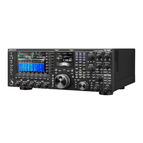
Kenwood TS-990S In-Depth Manual
Hide thumbs
Also See for TS-990S:
- Instruction manual (290 pages) ,
- Service manual (245 pages) ,
- Manual (62 pages)
Table of Contents
Advertisement
Quick Links
Advertisement
Table of Contents

Related Manuals for Kenwood TS-990S


Summary of Contents for Kenwood TS-990S
- Page 1 IN-DEPTH MANUAL...
- Page 2 There is always a risk of losing your important data by a transceiver failure, occurrence of an unforeseen contingency, • KENWOOD is a registered trademark of JVC KENWOOD erroneous operation or faulty behavior of the transceiver. Corporation. The data, such as the operating information, recorded audio, • Windows XP, Windows Vista , Windows 7, Windows 8 and messages, configuration data, and logs, must be backed up as ® ® ® ® the Windows logo are the registered trademarks of Microsoft necessary by yourself and stored in an external storage device ® Corporation in the United States and other countries. such as a USB flash drive. • .NET Framework is a registered trademark of Microsoft Corporation in the United States and other countries. URL AND CONTACTS OF JVC KENWOOD CORP. • IntelliMouse and IntelliPoint are registered trademarks of The latest URL and contacts of JVC KENWOOD Corporation Microsoft Corporation in the United States and other countries. at the time when this manual was written are described in • SHARC and the SHARC logo are registered trademarks of this manual. Due to changes of social circumstances or Analog Devices, Inc. the management environment, the URL and contacts of JVC KENWOOD Corporation may change from time to time.
-
Page 3: Table Of Contents
TABLE OF CONTENTS Protections ..............25 01 PROLOGUE SWR Protection ..............25 About the Release of the TS‑990S ........1 Overcurrent Protection ............25 Features of the TS‑990S ..........1 Thermal Protection and Fan Control ........25 Power Supply ..............26 02 ANTENNA SWITCHING CIRCUIT High‑Efficiency Large‑Capacity Power Supply Implemented .................26 Signaling Paths ..............2 Power Saving.................26 Using the Same Antenna Connector for the Main Band and Safety ..................26 the Sub Band ................2 Power Factor Correction (PFC) to Prevent Harmonics in Using Different Antenna Connectors for the Main Band and the Rectifier Circuit ..............27 the Sub Band ................3 Continuous Variable Rotations and the Cooling Fan . - Page 4 TABLE OF CONTENTS 07 SOFTWARE 08 TERMINAL Processor Connections ..........56 PADDLE and KEY Jacks ..........85 Dual TFT Display ............56 EXT SP1 and EXT SP2 Jacks ........85 PHONES Jack ............... 86 Main Screen ................56 Meter ..................57 KEYPAD Jack ..............86 Function Configuration Screens and Bandscope Screen ..58 METER Jack ..............87 Touch Screen ................58 ACC 2 Connector ............88 Sub Screen................58 OPTICAL IN and OPTICAL OUT Connectors ....89 Sub Scope .
-
Page 5: 01 Prologue
01 PROLOGUE About the Release of the TS‑990S Since the TS‑900 was launched in 1973, the Nine Hundred series of KENWOOD (TRIO) transceivers has been our flagship high‑end HF transceivers. Following the TS‑900, the TS‑930, TS‑940, and TS‑950 were launched. However, more than 20 years have now passed since the TS‑950SDX was launched. At the end of February 2013, we started shipping our long‑awaited new Nine Hundred series lineup. The TS‑990S is positioned as a top‑end transceiver in the KENWOOD HF transceiver lineup, both in name and reality. We accomplished the engineering of the TS‑990S enabling it not only to succeed the TS‑950 but also to be reputed as a flagship transceiver despite the TS‑990S being the last‑entered flagship transceiver in the marketplace. What we engineered with the most careful attention to position the TS‑990S as a flagship transceiver, is the fundamental transceiver performance. The performance includes not only the transmit and receive characteristics that can be measured as mathematical values but also what you will have been sensed that can be comprehensively received through actual transceiver operation. The detailed design aesthetic extends from the circuits and components all the way to the texture of the chassis and the operability of the panel. The TS‑990S has the functionality required for advanced DX operation as well as an eye‑catching dual TFT display and touch panel that let the user view a wide range of information. There are surprisingly many buttons on the TS‑990S, shown in the photographs in catalogs. However, we believe you will understand our design concept for the TS‑990S as transceiver when you see and operate it. The KENWOOD HF transceivers aim not only to receive signals from and transmit signals to locations further away, but also to transmit and receive signals with more natural sound. In other words, the TS‑990S has been designed as a flagship transceiver not only for DX’ers but also for those operators who seek for better sound quality. This in‑depth manual is written by the TS‑990S designers to describe the technologies and techniques used to implement the concepts mentioned above. We hope this manual will help you to have a deeper understanding of the TS‑990S. November 2013, KENWOOD HF Transceiver Development Team Features of the TS‑990S The TS‑990S is a HF/50 MHz all‑mode transceiver featuring a reception performance high enough to satisfy DX’ers all over the world and the world’s first dual TFT display , enabling higher operability and information feedback to the operator for better practical operation. ( As of August 2013, according to our research) The receiving circuits of the TS‑990S, a successor of the TS‑900, TS‑930, TS‑940, and TS‑950, realize dual band... -
Page 6: 02 Antenna Switching Circuit
02 ANTENNA SWITCHING CIRCUIT Signaling Paths The TS‑990S has 4 antenna connectors, ANT1 to ANT4, and the RX IN and RX OUT connectors that can be used for a reception‑dedicated antenna input or an external filter connection. There is more than one path from the antennas to the receiving circuits, and these paths can be changed according to the configuration. The paths from the antennas to the receiving circuits can be specified for each reception band in the main band and the sub band. The antenna terminals that are not specified are connected to GND. Using the Same Antenna Connector for the Main Band and the Sub Band BPF, etc. ANT 3 ANT 4 ANT 1 ANT 2 RX (OUT) RX (IN) Each Relay is in the Off state (inactive). -
Page 7: Using Different Antenna Connectors For The Main Band And The Sub Band
ANTENNA SWITCHING CIRCUIT 02 Using Different Antenna Connectors for the Main Band and the Sub Band BPF, etc. ANT 1 ANT 2 RX (IN) ANT 3 ANT 4 RX (OUT) Each relay is in the Off state (inactive). Splitter 3 dB loss MAIN FINAL Fig. 2... - Page 8 02 ANTENNA SWITCHING CIRCUIT Simply short‑circuiting the RX OUT connector, RX IN connector, and an antenna connector with the other receiver without using a splitter may start reception; however, it may cause impedance matching failure or a problem due to failure in isolation from the other receiver. OUT 1 Other Receiver Splitter OUT 2 ANT 4 RX (OUT) RX (IN) ANT 1 ANT 2 ANT 3 Splitter 3 dB loss MAIN FINAL Fig. 3 Example of Operation using the RX Antenna Function (Main Band) Fig. 4 Example of a Splitter Circuit “Example of a Splitter Circuit” shows a theoretical diagram of a splitter circuit. This circuit equally distributes signals entered from the IN terminal and sends them through the OUT1 and OUT2 terminals, resulting in a 3 dB insertion loss. Determine the number of turns for the transformer to be used according to factors such as the magnetic permeability of the core. A low‑capacitance capacitor may need to be connected to the input or output in parallel to correct the frequency characteristics. In the TS‑990S, a similar circuit is used for signal distribution to the main band and the sub...
-
Page 9: 03 Reception
03 RECEPTION Receiver Configuration The TS‑990S has two receivers; the main band receiver and the sub band receiver. This configuration enables dual band reception using the main band and the sub band even if two bands are in the same band or different bands. During transmission, the reception stops using both receivers. The bandscope circuit can select signals from either the main band receiver or the sub band receiver, regardless of the selected band, and show the status of IF signals selected and being transmitted (excluding FM modulated signals). Conversion Method Main Band Receiver It is important for a receiver to eliminate interfering signals through narrow filters at an earlier stage and pass desired signals to the subsequent circuits. Using filters with better selection characteristics for earlier elimination of interfering signals serves to prevent distortion in the subsequent circuits and improves practical anti‑interference characteristics. The first mixer, through which a number of interfering signals pass, needs to have high intercept point (referred to as IP hereafter) characteristics. In developing the TS‑990S main band receiver, implementation of roofing filters with excellent selection characteristics and high IP characteristics was the top‑priority. For the roofing filter implementation, the full down‑conversion method of the first IF frequency of 8.248 MHz is adopted (the “down‑conversion” method used in the system is not intended for a conventional configuration in which a high first IF frequency, e.g., the 73 MHz band is used but for a configuration in which a low first IF frequency, e.g., 8 MHz band or 11 MHz band, is used). The use of a low IF frequency allows filters with steep attenuation characteristics to be employed and performance sufficiently tolerant to adjacent interfering signals to be secured. The next issue was the bandpass filters placed in the front‑end block of the main band receiver. The use of a low first IF frequency allows interference on image frequencies and/or spurious reception to easily take place, thus it is necessary to place a number of bandpass filters with steeper attenuation characteristics. As shown in the table “Bandpass Filter Division in the Main Band Filter”, bandpass filters for 15 paths are used, and for the major amateur bands (1.8 MHz, 3.5 MHz, 7 MHz, 14 MHz, and 21 MHz), a toroidal coil with steep attenuation characteristics and high IP characteristics is used. Also, the bandpass filters for amateur bands including other WARC bands are designed for positive use of parts with high Q (quality factor) and distortion resistance characteristics. To eliminate distortion‑causing elements placed on the signaling paths in the front‑end block of the main band receiver, a switching method through relays is used to select the bandpass filter, pre‑selector, pre‑amplifier, post‑amplifier, and roofing filter for the major amateur bands. This also helps to reduce insertion loss and improve the isolation between the signaling paths. Table 1 Bandpass Filter Division in the Main Band Receiver Band Filter Bandwidth 30 to 522 kHz 522 kHz to 1.705 MHz 1.8 MHz 1.705 to 2.5 MHz 3.5 MHz... -
Page 10: Sub Band Receiver
03 RECEPTION The following block diagram shows the front‑end block or the main band receiver. Roofing Filters 270Hz 500Hz RF BPF 1 st Mixer 2.7kHz through through through 0/6/12/18dB 6kHz Pre Selector Pre Amp Post Amp 15kHz Fig. 5 Block Diagram of the Front‑end Block for the Main Band Receiver The signal received by the antenna enters the main band receiver through the antenna switching circuit. The bandpass filter for the selected band eliminates interfering signals outside the band, the received signal is amplified by a pre‑ amplifier and is then converted to the first IF signal (8.248 MHz) by the first mixer. The first mixer is described later. Through the post‑amplifier linked with the bandscope branching circuit and pre‑amplifier, the first IF signal enters a roofing filter that eliminates the adjacent interfering signals outside the band. The roofing filters are also described later. The “Block Diagram of the IF Stage for the Main Band Receiver” shown below illustrates the diagram of the blocks subsequent to the roofing filters. The first IF signal routes through the AGC amplifier and the first IF amplifier to the second mixer, which converts it to the second IF signal (24 kHz). The second IF signal enters the DSP as the baseband signal through the second IF amplifier, and routes through various signal processing such as demodulation after IF processing by the AGC, filters, audio signal processing, etc. In FM mode, the first IF signal (8.248 MHz) enters the FM system IC, and the detected AF signal enters the DSP for audio signal processing. IC12 FM AF AMP Switching AGC AMP (AF) - Page 11 RECEPTION 03 Table 2 Applicable Conditions for Down‑Conversion 1.8 MHz (1.705 to 2.1 MHz) 3.5 MHz (3.4 to 4.1 MHz) Band 7 MHz (6.9 to 7.5 MHz) 14 MHz (13.9 to 14.5 MHz) 21 MHz (20.9 to 21.5 MHz) Pass 2.7 kHz or less Bandwidth Mode SSB, CW, FSK, PSK The block diagram below shows the front‑end block of the sub band receiver. The signal received by the antenna comes into the sub band receiver through the antenna switching circuit. The bandpass filters divided for 12 paths eliminate the interfering signals outside the band, and a pre‑amplifier amplifies the signal and sends it to the first mixer. The first mixer has independent sections for down‑conversion and up‑conversion respectively, which are switched by the signaling path conditions. 30k~522kHz PRE OFF SRAT To 1st Mixer (Sub RX RF in) -6dB -12dB ~60MHz 522k~1.705MHz S6DB S12DB BC Trap 1.705M~60M Q219 Sub PRE AMP Fig. 7 Block Diagram of the Front‑end Block for the Sub Band Receiver...
-
Page 12: Pre-Selector
03 reception Fig. 9 Photograph of the Roofing Filter in the Sub Band Receiver Pre-selector The pre-selector is implemented to attenuate, by using a narrowband filter, the in-band interfering signals that cannot be eliminated by the bandpass filters in the front-end block of the main band receiver and to elicit the desired signals. The “Pre-Selector Unitary Resonance Circuit”... -
Page 13: New Mixer
RECEPTION 03 The “Frequency Response” figure shows an example of typical Pre‑selector Frequency Amplitude characteristics. Fig. 11 Frequency Response Pressing the [P.SEL] key to turn the pre‑selector on makes the tuning filter waveform‑shaped by the relay operation logic configured as the factory default, following the frequency displayed at the main band reception. Pressing and holding the [P.SEL] key shifts the center frequency of the tuning filter up to ±20 steps. For instance, when a strong adjacent interfering signal suppresses the desired signal, shifting the center frequency in the opposite direction of the interfering signals attenuates the level of the interfering signals instead of attenuating the desired signal, thus it effectively reduces interference as much as possible. New Mixer The first mixer was a part of the block on the main band receiver and was examined the longest. Double balanced mixers with conventional J‑FET implementation have been unable to fully satisfy the required IP3 characteristics. To satisfy the requirement, a mixer called the “H‑mode mixer”, which employs the double balanced grounded switch type that is different from conventional types, is employed for the first mixer. The circuit of the mixer can turn the GND terminating ends on the signaling paths On or Off, to minimize the mixer distortion. For the switch elements, bus switches are used and turned on/off only by low‑power local oscillator signals. For the RF input and IF output of the mixer, large balun transformers with distortion resistance characteristics are used, and the winding methods and materials of the cores with different magnetic permeability are carefully chosen and examined. Furthermore, after the mixer, a duplexer circuit is placed to stabilize the impedance of the roofing filters in a wider band. +2.5V 1st IF 8.248MHz +2.5V MLO1 8.278~51.752MHz Fig. 12 Double Balanced Grounded Switch Type Mixer... -
Page 14: Roofing Filters
03 RECEPTION Roofing Filters What is a Roofing Filter? This section describes the roofing filter, which is the most important in the main band receiver. The roofing filter is a filter placed at the ceiling, or the “roof” of the intermediate frequency (IF) circuit of the receiver. In other words, this represents a narrowband filter where the signal converted to the intermediate frequency first passes through. A received signal includes a number of strong adjacent signals other than the desired signal, thus attenuating the undesired signals in an early stage in a preceding circuit enables the signal to not be distorted in the subsequent amplifying circuit. The high intercept point obtained by the high‑performance first mixer gives full play to its ability in a frequency domain slightly distant from the desired signal attenuated by the roofing filter. If the level of adjacent signals inevitably passing through the roofing filter is high, it causes distortion to occur in the subsequent IF amplifier, mixer, and other circuits, and the dynamic range deteriorates on the adjacent frequencies. This is why the roofing filters must be narrowed to their minimum and attenuated to the steepest direction. For the main band, 8.248 MHz is selected for first IF frequency, and for the sub band with the down‑conversion setting, 11.374 MHz is selected for the first IF frequency; these first IF frequency settings enable filters with good attenuation characteristics in a narrowband and fewer characteristic changes by temperature. Note: ◆ For example, narrowband filters with a high frequency, e.g., 73 MHz, may be implemented, but such filters have large characteristic changes by temperature and cause problems such as increased attenuation, thus do not serve for practical operation. Main Band Roofing Filters Five roofing filters are used as narrowband filters of high IP characteristics implemented by the full down‑conversion method. The “Photograph of Roofing Filter in the Main Band Receiver” shows the roofing filters. In the photograph, the 15 kHz, 6 kHz, 2.7 kHz, 500 Hz, and 270 Hz bandwidth filters are mounted from the lower right side. In that order. The 15 kHz and 6 kHz bandwidth filters are 4‑pole monolithic crystal filters (MCF). The 2.7 kHz bandwidth filter is a 6‑pole monolithic crystal filter. The 500 Hz and 270 Hz bandwidth filters are structured as the ladder type to suppress in‑band insertion losses and steeply shape the adjacent out‑of‑band attenuation characteristics. The “Frequency response of the 500 Hz Bandwidth” and ”Frequency response of the 270 Hz Bandwidth” figures show the ladder filter frequency response. The roofing filters for the main band receiver can be selected regardless of operation mode (excluding FM mode). Pressing and holding the [FIL/SEL] (M) key opens the RX Filter screen on the main display. The screen allows you to select the roofing filter to be used. -
Page 15: Additional Roofing Filter
RECEPTION 03 Fig. 14 Frequency response of Fig. 15 Frequency response of the 500 Hz Bandwidth the 270 Hz Bandwidth Additional Roofing Filter The TS‑990S main band receiver has a slot to mount a roofing filter in addition to the five built‑in roofing filters. (We have no plan to commercialize additional roofing filters on our own.) Fig. 16 Additional Roofing Filter Mounting Slot If an additional roofing filter is mounted, change the default value of “Off” in Advanced Menu 6 “Bandwidth (Additional Roofing Filter)” to your desired filter bandwidth, and then press and hold the [FIL/SEL] (M) key to open the RX Filter screen. In the screen, change the configuration for “Roof” to “Add.” to enable the additional roofing filter. If “Auto” is set to “Roof”, the additional roofing filter is preferentially selected depending on the IF filter bandwidth. Concerning the built‑in roofing filters, the PIN diode‑type attenuator at the IF stage corrects the gain, causing no difference in S meter needle deflection, whether a filter is applied or not. But, if an additional roofing filter is used, it is necessary to correct the S meter needle deflection by a difference of the insertion loss. To receive a signal with a stable signal strength, change the attenuation of the additional roofing filter in Advanced Menu 7 “Attenuation (Additional Roofing Filter)”. The “Electrical Specifications” table shows the additional roofing filter electrical specifications. The “Dimensions (Reference)” diagram shows the additional roofing filter dimensional diagram (reference). Table 4 Electrical Specifications Center Frequency 8.248 MHz Bandwidth (‑6 dB) 300 to 3500 Hz Terminating Impedance 50 Ω Insertion loss 8 dB or less... -
Page 16: Adjacent Interference Characteristics
03 RECEPTION 47.5 62.0 ϕ1.0 ~ 1.2 14.45 11.4 17.5 16.1 5.15 23.75 R0.7 23.35 No part can be mounted on the reverse. 3.7 x 5.3 Fig. 17 Dimensions (Reference, Unit: mm, top view) Adjacent Interference Characteristics The “IP3 Characteristics Comparison” graph shows a comparison between the TS‑990S main band receiver (orange) and the receiver of a conventional transceiver (gray). It indicates that the IP3 characteristics are improved to the +40 dBm level and uniformly settled to adjacent interference signals in the range of 2 to 10 kHz from the reception frequency. In addition, the 110 dB class dynamic range, which exceeds the 105 dB class of the TS‑590S, has been achieved. Fig. 18 IP3 Characteristics Comparison Note: ◆ The horizontal axis is the separation to the desired signal of the interference signal frequency (2 waves). At 10 kHz, interfering signal 1 is the +10 kHz reception frequency, and interference signal 2 is the +20 kHz reception frequency. -
Page 17: Agc Circuits
RECEPTION 03 AGC Circuits Analog AGC Circuits To achieve high adjacent dynamic range characteristics, an analog AGC circuit is used together to make the A/D Converter work to its performance limit. The AGC circuit is required to have low noise and a wide dynamic range, wide control range, and linearity to the control. The TS‑990S implements high‑precision AGC response characteristics with an AGC circuit in which a dual‑gate MOSFET is used (shown in the diagram “AGC Circuit with a Dual‑Gate MOSFET”) and correction is made by DSP. Fig. 19 AGC Circuit with a Dual‑Gate MOSFET The graph below shows the AGC response characteristics to a control voltage in the circuit configuration with a dual‑ gate MOSFET. Sufficient control range, dynamic range, and linearity are secured. Dual Gate MOSFET Fig. 20 AGC Response Characteristics to a Control Voltage Optimized Gain Distribution The mixer, which is the key block in the main band receiver and is newly developed, has relatively larger conversion loss than that of conventional mixers. Therefore, the circuit is structured to work in conjunction with a post‑amplifier, which is placed in the mixer output, during operation of the pre‑amplifier. Pressing the [P.AMP] key improves the reception sensitivity by approximately 14 dB by pre‑amplifier 1 and the post‑amplifier in a reception band below 21.5 MHz and approximately 18 dB by pre‑amplifier 2 and the post‑amplifier in a reception band above 21.5 MHz. The attenuation outside the band is fully obtained by the roofing filters with good selectivity. Therefore, the analog AGC circuit and high‑gain IF amplifier are placed in a later stage so that undistorted IF signals are supplied as baseband signals to the DSP. -
Page 18: Deflection Of The S Meter Needle
03 RECEPTION Deflection of the S Meter Needle The IARU (International Amateur Radio Union) standard scale requires ‑73 dBm as the S meter level to point S9. However, concerning the S meter needle deflection, on all our products, the S meter level is ‑81 dBm to point S9 in the 14 MHz band while a pre‑amplifier is on. The TS‑990S also provides S meter needle deflection familiar to operators using a conventional model. Turning off the pre‑amplifiers lowers the gain and the S meter needle deflection. The gain changes by a pre‑amplifier by approximately 12 dB in the amateur bands up to the 21 MHz band and by approximately 20 dB in higher bands. The “S Meter Levels (Reference)” table shows the indicated levels of the S meter. (The S meter level is adjusted to point S1, S9, or S9+60 in the 14/50 MHz bands.) In FM mode, you can select the same configuration (High) as that has been configured for conventional models, or a lower value enabling to lower the S meter sensitivity, through Menu 0‑08 “FM Mode S‑meter Sensitivity”. Table 5 S Meter Levels (Reference) 0.03 to 21.5 S Meter 21.5 to 60 MHz FM (High) FM (Low) S1 (3 dots) ‑107.0 dBm ‑114.0 dBm ‑117.0 dBm ‑117.0 dBm S3 (11 dots) ‑100.5 dBm ‑107.5 dBm ‑114.4 dBm ‑112.8 dBm S5 (19 dots) -
Page 19: Rf Gain Adjustment
RECEPTION 03 RF Gain Adjustment KENWOOD HF‑band transceivers are designed with our consistent philosophy to balance the levels, such as the sensitivity, S meter needle deflection, pre‑amplifier gain, gain correction, and other factors. If the input level from an antenna is low, (internal) noise may be conspicuous. If noise is conspicuous, reducing the IF gain can lower the noise level. For that purpose, the [RF] knob is provided. Rotating the [RF] knob counterclockwise reduces the IF gain and consequently lowers the noise level. Slightly lowering the gain does not change the reception sensitivity. The S meter shows the gain reduction by the AGC and the [RF] knob, thus the S meter needle deflects by the gain reduction. In the range the AGC is applicable, the S meter sensitivity does not change. Placing the [RF] knob to the 3 o`clock position reduces the IF gain by approximately 6 dB from the maximum and reduces the noise level at no signal by approximately 6 dB. The gain reduction causes the S meter needle to deflect closer to S3. A 6 dB gain reduction causes the sensitivity to change little, and the reception sound volume does not change with reception of a usual signal that makes the S meter needle deflect. If the noise level is noticeable, adjust the RF gain. AGC Off The AGC time constants for such as the attack time, release time, and hold time are optimized for a practical radio waves state. However, for reception of a signal easily buried in noise, turning the AGC off may occasionally increase its performance. In such a case, the AGC can be disabled with a press of the [AGC OFF] key. With the AGC inactive, the signal level will not be controlled to be the certain volume level, and the speaker may emit very loud sounds. This is why a confirmation message appears before the AGC is turned off to prompt attention to loud sounds. Before turning the AGC off, you must adjust the RF gain to a signal level that makes the S meter needle deflect. Rotate the [RF] knob counterclockwise to lower the RF gain, letting the S meter needle deflect slightly wider. This prevents loud sounds from being emitted while the AGC is inactive. If a large signal is entered while the AGC is inactive, the S meter needle deflects up to the level specified for the RF gain and the reception sound volume increases up to a certain level. However, if this level is exceeded, the reception audio volume reaches its limit and sudden distortion takes place. This is intended to set limits so that the allowable levels are not exceeded in the D/A converter and through signal processing. -
Page 20: Noise Blankers
03 RECEPTION Noise Blankers Features of the NB1 and NB2 The TS‑990S has two noise blankers; NB1 for analog processing and NB2 for digital processing by DSP. NB1 is effective for short‑cycle pulses, such as ignition noise. NB2 is effective for noise that the analog noise blanker (NB1) cannot follow. The following block diagram shows the analog noise blanker (NB1). Buffer NB AMP2 NB AMP3 NB AMP4 Buffer Noise Detection Switching Mute Signal NB AGC Noise Blanker Threshold Level Fig. 23 Noise Blanker Circuit (NB1) Block Diagram NB1 has the circuit configuration inherited from that of conventional models, which is effective for weak noise. A pulse signal after passing through a narrowband filter changes its noise waveform, increasing the pulse width. Thus, at the roofing filter input stage, which is not subject to influence of pulse noise, signals are picked up and switch circuits operate. For example, if a pulse with a short cycle is entered as shown in diagram 1, the AGC in the noise blanker circuit does not react to it, thus the switch functions and a muted signal will be present. -
Page 21: Auxiliary Circuits
RECEPTION 03 Auxiliary Circuits Medium Wave Band Sensitivity Risers Just as in conventional transceivers, the TS‑990S has attenuators of approximately 20 dB for the medium wave band (522 kHz to 1.705 MHz) (as the factory default, the sensitivity is lowered by approximately 20 dB by the attenuators). In the medium wave band, there are a number of strong radio waves and there may be medium wave band input excessive for low‑band antennas. The inserted attenuators are intended for clear reception with less distortion even if such strong medium wave band signals are received. The attenuators are placed respectively for the main band and the sub band, and the signal can bypass the attenuator after switching the jumper pins on the board allowing it to increase the sensitivity. The “Main Band Jumper Pin Locations” image shows the main band attenuator jumper pins and the parts around them on the RX unit. The “Sub Band Jumper Pin Locations” image shows the sub band attenuator jumper pins and the parts around them on the TX‑RX unit. Detach the TS‑990S lower case to access the TX‑RX unit. To access the RX unit, detach the center shield plate. (Before detaching the lower case, be sure to first detach the upper case. After finishing the jumper pin configuration, first attach the lower case, and then attach the upper case. Otherwise, the cases may be damaged.) Table 6 Medium Wave Band ATTs Main Band Sub Band NORM (ATT: 20 dB) CN 60 CN 220 DX (ATT: Thru) CN 50 CN 210 Fig. 25 Sub Band Jumper Pin Locations Fig. 24 Main Band Jumper Pin Locations The jumper pins are placed in the”NORM” position at shipment. Placing the jumper pins to the connectors for “DX” bypasses the attenuators and raises the medium wave band sensitivity by approximately 20 dB. Fig. 26 Medium Wave Bandpass Filter Characteristics... -
Page 22: 04 Transmission
04 TRANSMISSION IF Circuit for Clean and Stable 200 W Output Power A signal modulated and multifariously processed in the DSP is fed as the 24 kHz transmit first IF signal by a D/A converter, and a mixer IC converts it to 10.695 MHz. The second IF signal of 10.695 MHz passes through an IF filter with a 6 kHz bandwidth at which undesired frequency components outside the band are attenuated, and is then amplified. Next, the signal goes through a gain control circuit that corrects the gain difference by band, enters a TX/RX mixer, and is then converted to the 73.095 MHz third IF signal. After that, the signal passes through a gain control circuit that corrects the signal gain to the required level for the specified transmit power. The signal then passes through a filter that eliminates unwanted spurious components and an ALC circuit that controls the signal to be a stable transmit power, and enters a mixer circuit for conversion to the desired transmit frequency. If there is no key‑down during operation in CW mode, the amplifier gain is lowered. As described above, fine gain control in compliance with the situation implements low‑noise and high‑quality transmit signals. The signal converted to the desired transmit frequency passes through a bandpass filter to eliminate spurious signals, so as not to generate an interfering signal outside the transmit bandwidth, and is amplified to a certain level and sent to the final circuit. The drive signal generated through the process is also available from the DRV terminal (if the DRV output is enabled). FET Final Amplifier Circuit The TS‑990S final amplifier employs the well‑reputed MOS FET VRF150MP (Pch 300 W) and is configured with a push‑ pull system. The FET, supplied by Microsemi Corporation, is paired, with two VRF150s of the same rank and carefully chosen by the Vth characteristics. By connecting FETs of matched characteristics in the push‑pull system, fine IMD characteristics and high stability can be achieved. The drive amplifier employs a MOS FET RD100HHF1 and the pre‑ drive amplifier employs a MOS FET RD06HHF1. The final amplifier circuit is configured with 50 V power and enables continuous operation with low distortion and stability. Fig. 27 Final Devices and Final Amplifier The Transmit IMD Characteristics (14.2 MHz, 200 W output power) and Transmit Spurious Response (14.2 MHz, 200 W output power) graphs show the IMD characteristics and harmonic spurious response. The graphs prove superb anti‑ distortion characteristics and clean output power. Fig. 28 Transmit IMD Characteristics Fig. 29 Transmit Spurious Response (14.2 MHz, 200 W output power) -
Page 23: High-Speed Relay-Controlled Antenna Tuner
TRANSMISSION 04 High‑speed Relay‑controlled Antenna Tuner The TS‑990S has a high‑speed relay‑controlled antenna tuner, which digitally controls in a combination of capacitors of different capacitance through switching relays. The digital control achieves high‑speed tuning. The antenna tuner employs parts durable for operating at 200 W and has dedicated cooling fans to secure continuous operation at 200 W. Fig. 30 Automatic Antenna Tuner Circuit Linear Amplifier Control There are two control methods for switching between transmit and receive in the linear amplifier or the transverter; one method is by using a relay for the linear amplifier and the other is by using the RL pin. Both methods allow you to send the control signal via the REMOTE connector. The linear amplifier control can be enabled in the Advanced Menu, as described later. REMOTE Connector The REMOTE connector is a 7‑pin DIN type connector, the same as our conventional transceivers. The REMOTE Connector Pin Assignment illustration shows the signaling paths allocated to the REMOTE connector pins. (RX) (TX) Active High/ Active during TX: 12V Active Low/ Active during TX: Low Fig. 32 REMOTE Connector Terminal Description Fig. 31 REMOTE Connector Pin Assignment Table 7 Terminal Descriptions for the REMOTE Connector Terminal No. -
Page 24: Configurations In The Advanced Menu
04 TRANSMISSION ● Use of the Linear Amplifier Control Relay The TS‑990S linear amplifier control relay functions on transmission if “Active High + Relay Control” has been selected from Advanced Menu 11 or 12. The linear amplifier control relay assumes that the TL‑922 (discontinued) is standing by and can be connected as‑is to the TL‑922. For a linear amplifier that stands by with a voltage application or a short‑circuit to ground, disable the relay control and make it standing by using the RL terminal as described later. ● Use of the RL Terminal In addition to a logic to output 12 V on transmission, following the configuration in the Advanced Menu as described later, in the same manner as conventional transceivers, a logic for short‑circuiting to ground on transmission by an open drain is added to the RL terminal (pin 7). By this, to use a linear amplifier that is placed in the transmit state with the low state logic for transmit control, the linear amplifier can be used without externally adding a transistor to reverse the logic. When transmission starts while the RL terminal has been set to “Active High”, the transistor switch shown in the “REMOTE Connector Pin Assignment” is turned On and 12 V is diverted (10 mA or less). “Active High” indicates that the logic is high while the circuit is active. If a linear amplifier which can be switched to the transmit state upon detection of the voltage is connected, configure “Active High” for the RL terminal. When transmission starts if “Active Low” has been configured for the RL terminal, the FET switch shown in “REMOTE Connector Pin Assignment” switches to a short‑circuit to ground. “Active Low” indicates that the logic is low while the circuit is active. The linear amplifier, which can be switched to the transmit state while the signal pulled up by the linear amplifier is being short circuited to ground, can be connected. If such a linear amplifier is connected, configure “Active High” for the RL terminal. However, the amount of withstand voltage and current are not large (DC 15 V or less, 10 mA or less), thus it is not possible to directly drive a relay in this circuit or to connect those which are activated with high voltage, such as an evacuated‑tube type linear amplifier (e.g., TL‑922). In such a case, use relay contacts alternatively. Configurations in the Advanced Menu To control the linear amplifier, configure the settings in the Advanced Menu. -
Page 25: Alc
Switch RF Power RF Power 45 ms Fig. 33 Timing Charts: When the TX Delay Control is Not Selected (Left) and Selected (Right) If a linear amplifier that conforms to full break‑in and switches to the transmit state upon application of approximately +12 V voltage is connected, select “Active High” from Advanced Menu 11 “Linear Amplifier Control (HF Band)” and Advanced Menu 12 “Linear Amplifier Control (50 MHz Band)”. If an external linear amplifier that does not conform to break‑in and takes time to switch the internal relay contacts, e.g., the TS‑922, is connected, select “Active High + Relay & TX Delay Ctrl” from Advanced Menu 11 and Advanced Menu 12. This configuration extends the duration of time from when the transceiver is placed in the transmit state until radio waves are practically transmitted so that the linear amplifier relaying will switch and then transmit the radio waves. If full break‑in is active in CW mode, the duration of time prior to a transmission is not extended. Note that selecting “Active High + Relay & TX Delay Ctrl” or “Active Low + TX Delay Control” from Advanced Menu 11 and/or Advanced Menu 12 extends not only the duration of time until a transmission starts but also the duration of time until reception begins, so as to reduce the click noise at the moment of switching. Note: ◆ Large‑sized relays generally tend to take time to start switching after energizing and have a long duration of time in which chattering may take place at the moment of switching. If transmission starts before the contacts switch to the transmission side, the SWR will increase until the switching finishes, thus the TS‑990S activates a protection circuit to momentarily reduce the transmit power. In addition, there is a case where the microphone may pick up a large operating sound of relay switching and the sound causes transmit signals to be transmitted. There is also another case where contact switching in the reception side after reception starts may cause a strong clicking noise. Selecting “Active High + Relay & TX Delay Ctrl” or “Active Low + TX Delay Control” may serve to prevent such problems. For use with a linear amplifier or transverter, it is possible to connect an external device to the ALC terminal (pin 6), intending proper transmit power control. If the transmit power reaches the range to be restricted from the external device standpoint, the ALC signal shifts the voltage to the negative side (for KENWOOD transceivers). External devices generally have voltage adjustment variable resistors. On the TS‑990S, applying a negative voltage (between ‑7 V and ‑10 V) to the ALC terminal reduces the internal gain. The operating point is described later. As described above, conventionally it has been common to enter the ALC signal from a linear amplifier to control the automatic level. However, in order to prevent excessive input to the linear amplifier, it is recommended to make a preliminary adjustment to the appropriate transmit power. If the transmit power is set by the ALC while the full transmit power is present in the transceiver, excessive power is applied to the linear amplifier before the ALC voltage is applied from the linear amplifier, resulting in linear amplifier damage. -
Page 26: Transmit Power Limiter
04 TRANSMISSION ● Recommended Operation Set the maximum transmit power, that can be entered to the linear amplifier, to the TS‑990S in advance. The ALC control in the transceiver activates at high‑speed, thus it can limit the output power without receiving an ALC signal from the linear amplifier. The transmit power limiter described later is useful for this. As configured as described above, apply the ALC signal of the linear amplifier to the ALC terminal of the TS‑990S. If the linear amplifier has to limit the transmit power, for example, in the case where the transmit power of the TS‑990S is increased by a false operation, this protects the linear amplifier. Transmit Power Limiter The transmit power limiter prevents the transmit power from exceeding the pre‑configured transmit power level. Pressing the [MAX‑Po] (F) key opens the TX Power Limit screen. The screen allows the configuration of the transmit power by band. Continuously rotating the [PWR] knob clockwise increases the transmit power to the configured maximum. Consequently, transmit power limit for use in DATA mode and transmit power with TX tuning can also be configured. An external device such as a linear amplifier may have different gains or withstanding input powers by band, thus the required transmit power varies in most cases. The TX Power Limit screen allows the configurations for the transmit power by band. If the maximum transmit power has been configured on the screen, this eliminates troublesome transmit power adjustment with the [PWR] knob each time the band is changed. Fig. 34 Setting Screen for the Max Power Limiter Function Selecting “ANT1” for the antenna connector when an external antenna tuner is connected limits the maximum transmit power to 100 W. Even if the transmit power limiter is set to 100 W or higher, “00 W” appears on the lower line of the [MAX‑Po] (F) key and the transmit power on the main screen (top center). Note: ◆ Transmit power cannot be configured individually for each antenna connector (ANT1 to ANT4). ALC Operation when an External Device is Connected "Connection Block to an External Device for ALC Signal Input" shows the block diagram of a signal circuit to enter the TS‑990S ALC signal from an external device and control the TS‑990S internal ALC amplifier. -
Page 27: Drv Terminal
TRANSMISSION 04 Fig. 35 Connection Block to an External Device for ALC Signal Input Fig. 36 Change of DRV Output Level by the ALC Voltage ● Operation on an ALC Signal Input from an External Device If the microphone gain and carrier level are adjusted to optimize the ALC meter needle deflection while no ALC signal is present from an external device, applying an external ALC signal results in more feedback control for the ALC. Therefore, the increase causes the ALC meter needle to deflect wider. In that case, rotate the [PWR] knob counterclockwise while viewing the ALC meter needle deflection or readjust the microphone gain and carrier level. DRV Terminal The output level from the DRV connector is approximately 0 dBm (1 mW). Depending on the configuration for the transmit power, the output level can be lowered to approximately 1/20. To make the output level lower, rotate the [CAR] knob in CW, FSK, PSK, or AM mode, or rotate the [MIC] knob (microphone gain) or [PROC OUT] knob (speech processor output level) in SSB mode. The level for the output signal from the DRV connector is insufficient to be transmitted directly through an antenna. Operation with a transverter or connection to the high‑gain linear amplifier allows operation in each amateur band including the 135 kHz band. The following graphs show the spurious response in the 14 MHz band and spurious response in the 135 kHz band on the DRV connector. The harmonic level also changes upon change of the level to 0 dBm, ‑10 dBm, and ‑20 dBm. DRV outputs not passing through a low‑pass filter may include a lot of harmonic components. For transmission, eliminate such harmonic components through a low‑pass filter as needed after signal amplification. Alternatively, lowering the level for the transmit power configuration or applying the ALC signal from the REMOTE connector to limit the DRV connector output level can reduce distortion. - Page 28 04 TRANSMISSION Fig. 37 Spurious Response: Fig. 40 Spurious Response: 14.175 MHz, 0 dBm 136 kHz, 0 dBm Fig. 38 Spurious Response: Fig. 41 Spurious Response: 14.175 MHz, ‑10 dBm 136 kHz, ‑10 dBm Fig. 39 Spurious Response: Fig. 42 Spurious Response: 14.175 MHz, ‑20 dBm 136 kHz, ‑20 dBm...
-
Page 29: Protections
TRANSMISSION 04 Protections The TS‑990S employs a final amplifier circuit configuration for a 200 W transmit power output with sufficient margins. Consequently, protections against large currents and excessive heating are provided, taking account of safety. SWR Protection If the antenna SWR (standing wave ratio) is high, efficient radio wave radiation is disturbed, and distortion may occur in the final circuit by reflected waves, or the TS‑990S, its antennas, or in a worst case scenario, other components may be damaged. To prevent such a problem from occurring, a protection circuit is implemented to reduce the transmit power to reflected waves. The protection circuit starts reducing the transmit power when the SWR becomes 1.5 or higher. Overcurrent Protection A protection circuit is implemented to monitor currents in the final amplifier and prevent currents over a specified level from passing through. Thermal Protection and Fan Control In the TS‑990S, two final amplifiers are mounted, and thermistors are placed near the amplifiers. The thermistors sense the temperature. The cooling fan for the final amplifier block switches its rotations in 3 steps according to the detected temperature (antenna tuner fan: 2 steps, AC/DC power supply fan: variable). The “Final Amplifier Fan Activation Temperatures (Detected) and Cooling Fan Rotation Speeds” table shows the cooling fan rotation speeds for the cooling fan activation temperatures. The antenna tuner fan is designed to follow the rotation speed of the final amplifier fan and activates only when the antenna tuner is active. If the final amplifier temperature appears to increase more, a warning message appears on the main screen, and the transmit power is controlled or the transmission is stopped. The transceiver is then placed in the receive state so as to prevent it from being damaged. Additionally, the cooling fan rotation pulses are detected to monitor whether all the cooling fans including the final amplifier fan are running normally. If a cooling fan is not rotating normally, an error message appears on the main screen and some functions will be restricted to secure the TS‑990S. Table 9 Final Amplifier Fan Activation Temperatures (Detected) and Cooling Fan Rotation Speeds Cooling Fan Rotation Speed Final Amplifier Fan Activation Temperature (Detected) Final Amplifier Fan Antenna Tuner Fan... -
Page 30: Power Supply
04 TRANSMISSION Power Supply High-Efficiency Large-Capacity Power Supply Implemented In the TS‑990S, a large‑capacity current‑resonance‑type switching power supply unit is implemented for stable 200 W transmit power operation. In comparison with conventional transformer types, its load efficiency is higher (83% typical on AC 100 V 200 W transmission) with less heating and less power consumption. Fig. 43 High‑Efficiency Large‑Capacity Power Supply Power Saving The TS‑990S has another power supply circuit dedicated for the main microprocessor, which is different from those sourced for the TX/RX. In low power consumption mode, the standby power is secured to 0.5 W or less. This conforms to international energy regulations. Safety The TS‑990S conforms to international safety standards and provides the following protection functions for safety operation. ● Overcurrent Protection All power supply output currents are subject to monitoring, and if an overcurrent is detected, intermittent output begins to drop the output voltage. ● Thermal Protection The temperature in the power supply unit is subject to regular monitoring. When the temperature rises excessively, transmission stops, and if the temperature rises more, the power supply shuts down to secure the safety operation. -
Page 31: Power Factor Correction (Pfc) To Prevent Harmonics In The Rectifier Circuit
TRANSMISSION 04 Power Factor Correction (PFC) to Prevent Harmonics in the Rectifier Circuit A switching power supply typically produces large harmonics in a rectifier circuit by its switching operation, causing reduction of the power factor, and harmonics reflected back to the AC input side may cause noise and other disturbances to external devices. The TS‑990S employs a rectifier circuit of the Power Factor Correction (PFC) method to make current waveforms close to the sine wave in order to prevent reduction of the power factor and disturbances due to power supply harmonics and conform to international power supply harmonics regulations. Fig. 44 Difference in Rectified Waveforms with/without Application of Power Factor Correction (PFC) Continuous Variable Rotations and the Cooling Fan The temperature of the switching power supply block is subject to regular monitoring, and the cooling fan rotations are continuously changed for the best‑suited cooling, increasing the cooling efficiency and reducing the cooling fan noise. DC/DC Converter For the power feed to the respective blocks, a DC/DC converter is employed. In comparison with a regulator for power feed on conventional transceivers, it generates less heat and requires less power consumption. -
Page 32: 05 Local Oscillator
05 LOCAL OSCILLATOR DDS and PLL System The local oscillator circuit in the TS‑990S is configured to give best‑suited characteristics to signals to be processed by the VCO division type and the DDS (Direct Digital Synthesizer) direct system (switchable) for the main band receiver, DDS system for the sub band receiver, and PLL system for the transmission block. First Local Oscillator for the Main Band Receiver The first local oscillator for the main band receiver is not a DDS direct system but a conventional VCO/PLL system (excluding the 10 MHz, 28 MHz, and 50 MHz bands). Generally, the VCO/PLL system is good for C/N characteristics on distant carrier frequencies and superior in spurious response by the effect of the filter in the PLL loop, while it tends to be disadvantageous for characteristics of the adjacent carrier to noise ratio. In the TS‑990S main band receiver, down converting all bands enables it to lower the local oscillator frequencies. Consequently, the first local oscillator for the main band receiver newly employs the division type that oscillates the conventional‑type VCO/PLL output signals using a higher frequency than the desired frequency and then divides the output signals. Theoretically, the C/N characteristics of the VCO/PLL output signals are improved by the effect of division at the ratio of 20*log (division ratio) (1/10 division maximum: 20*log (1/10) = ‑20 dB). Block Diagram of First Local Oscillator for Divider Main Band RX Circuit 82.78 ~ 115.48 ~ 1.8/3.5/5M …... -
Page 33: First Local Oscillator For The Sub Band Receiver
LOCAL OSCILLATIOR 05 First Local Oscillator for the Sub Band Receiver The first local oscillator for the sub band receiver, which is refined and diverted from the local oscillator circuit of the TS‑590S, directly feeds output signals to a mixer from a 14‑bit DDS which has superior adjacent C/N characteristics. During the down‑conversion, the oscillating frequency is lower than that of the up‑conversion method, and the C/N characteristics for the output signals will be improved further, resulting in fine reciprocal mixing characteristics. Sub Band Local Oscillator C/N 14.1 MHz IF: 11 M Fig. 47 C/N Characteristics of the First Local Oscillator for the Sub Band Receiver Local Oscillator in the Transmit Block In comparison with the first local oscillator using a conventional VCO/PLL system, the first local oscillator using a DDS system has better characteristics of the adjacent carrier to noise ratio; however, as a transmitter, good C/N characteristics on distant carrier frequencies are required. If there is a strong signal present using a distant carrier frequency, and if noise affects the desired signal by poor characteristics of the distant carrier to noise ratio of the signal, the noise causes interference to reception of the signal. On a local station or those participating a contest in the multi‑band, interference of reception by noise may occur in some cases. Considering the 200 W output power of the TS‑990S and the market demand emphasizing the manner not to disturb other stations, the TS‑990S employs a VCO/PLL system for the local oscillator circuit in the transmit block, achieving significant C/N characteristics for distant carrier frequencies. -
Page 34: Reference Frequency Generator Circuit
05 LOCAL OSCILLATOR Reference Frequency Generator Circuit The TS‑990S employs a TCXO for generating the reference frequency enabling a frequency stability of 0.1 ppm (0 to 50°C/32 to 122°F). Fig. 49 TCXO (Temperature Compensated Crystal Oscillator) Frequency Stability (Referenced to +25°C) Fig. 50 Frequency Stability Application of the OCXO to the reference frequency generation improves the frequency stability. However, the OCXO serves for high stability by keeping a high internal temperature, and power consumption of a few more watts is required. Additionally, the OCXO requires time to stabilize the internal temperature. In the case of a cold start, it takes several minutes to stabilize the internal temperature. To be ready for operation immediately after the power is turned ON, it needs to be energized at all times. On the other hand, the TCXO fine‑adjusts the output frequency to a temperature that the internal temperature sensor detects. This allows the reference frequency stability to be secured, resulting in low power consumption (TCXO power consumption: 7.92 mW, max.). Frequency Stability Time (Cold Start) Fig. 51 Comparison of Power‑up Characteristics of the TS‑990S and Transceivers with an OCXO Implemented... - Page 35 LOCAL OSCILLATIOR 05 Furthermore, the TCXO has a short start‑up time (400 ms or lower for the 10 MHz reference signal output) to operate following the ambient temperature, the TS‑990S can be used immediately even if it is not energized while the TS‑990S is not in use. Considering the reference frequency generator circuit characteristics and global energy‑saving approaches, the TCXO is employed for the TS‑990S. If higher accuracy and stability than those present by the reference frequency generator circuit is demanded, enter a 10 MHz (‑10 to +10 dBm) reference signal to the REF I/O connector from an external reference oscillator. With this, the frequency accuracy of the external reference oscillator is applicable to the operation. Also, the 10 MHz reference signal with the accuracy of the reference frequency generator circuit of the TS‑990S can be generated from the REF I/O connector. To enter the reference signal to the REF I/O connector, select “Input” from Advanced Menu 4 “REF I/O Connector Configuration”. To generate the TS‑990S reference frequency from the REF I/O connector, select “Output” from Advanced Menu 4. 1 MHz Reference Output Time (from power key voltage detected) Fig. 52 REF I/O Output Starting Characteristics...
-
Page 36: 06 Dsp
06 DSP The TS‑950 series HF transceivers were the world’s first amateur radios with built‑in DSPs. The TS‑870 achieves, with DSP, all IF processing including the IF AGC processing for controlling the received signal level and the steep IF filter. The TS‑590S provides evolved IF AGC processing for fine sound quality durable over long‑time operation and functions for noise/interference rejection and boasts of top‑level reception characteristics by means of DSP. We have been providing “Quality” in communications that cannot be realized only by analog circuits. The development concept of the DSP for the TS‑990S is the very compilation of our traditional techniques. Achievements of various functions are important; however, it is DSPs that represent our positive attitude towards “Quality”. Features of TS‑990S DSP Technologies • Three 32‑bit floating‑point DSPs are implemented for the main band RX/TX, sub band RX, and bandscope, respectively. • The IF AGC processing intends to pursue the natural audio quality with the comprehensive matching of analog circuits, roofing filters, and IF filter with digital signal processing. • The bandscope processing materializes high resolution and high‑speed sweeping. DSPs and Peripheral Hardware Fig. 53 DSP Hardware Block Diagram The DSPs that are kernels of the digital signal processing are 32‑bit floating‑point DSP SHARC processors made by Analog Devices Inc. and provide better arithmetic characteristics than the 32‑bit floating‑point DSPs employed in the TS‑590S. There are three SHARC processors (referred to as DSPs hereafter) built in the TS‑990S. - Page 37 DSP 06 Table 10 Description of the DSPs Name DSP Type Operation Clock Functions TXMRX DSP ADSP‑21363 331.776 MHz Main band reception, transmission, RTTY/PSK31/PSK63 encoders Sub band reception, audio output control, voice guidance, optical SRX DSP ADSP‑21369 258.048 MHz digital signal I/O SCP DSP ADSP‑21363 331.776 MHz Bandscope, audio scope, RTTY/PSK31/PSK63 decoder The DSP for transmission and main band reception is called the “TXMRX DSP”, the DSP for sub band reception and audio output processing is called the “SRX DSP”, and the DSP for the bandscope and decoding in RTTY/PSK31/PSK63 modes is called the “SCP DSP”. The TXMRX DSP and SRX DSP are placed in the DSP unit and DSPs are linked together and process the transmit and receive signals. The application of high‑processing‑ speed DSPs with large built‑in memory achieves functional enhancement such as improved IF AGC processing performance, a new interference rejection capability, improved IF filter shaping factors, speech processor IF implementation, and RTTY/PSK31/PSK63 encoder/ decoder implementation. Fig. 54 TXMRX DSP Also, implementation of the digital interface enabling the digital audio signal input and output via the Optical connectors is nice for those who have a keen interest in audio signal quality. By using an optical digital cable, optical digital signals can be sent via and received from an external device, without using an analog path. Consequently, digital...
-
Page 38: Signal Processing In The If Stage
06 DSP Signal Processing in the IF Stage The IF AGC processing for signal reception is the core of the TS‑990S. In the TS‑870, TS‑2000S, and TS‑590S, the IF AGC processing is the most actively innovated algorithm in the DSP signal processing and the tuning in the analog stages. We have found new tasks each time we create an innovation and solve them through hardships. The IF AGC processing we have been innovating through inheritance of our technological tradition represents our KENWOOD tones. IF AGC Processing As described above, the TS‑990S can simultaneously receive two bands by using the main band and the sub band. The basic scheme (block) of the IF AGC processing is the same for both the main band DSP and the sub band DSP. However, concerning the analog‑step frequency configuration, down‑conversion is applied for the main band and conditional down‑conversion/up‑conversion switching system is applied for the sub band, and the applicable roofing filter types are different. For both the main band and the sub band, the passband width of the preceding stage (analog stage) may be wider than the final passband width of the DSP. The IF AGC processing was designed carefully so as to influence interfering signals to the desired signal. The analog circuit characteristics of the main band are different from those of the sub band, thus their response characteristics are respectively tuned. Fig. 57 IF AGC Processing Block Diagram AGC loops are placed before and after the interference rejection, such as an IF filter, manual notch filter, etc. The AGC loop of the preceding stage functions to prevent signals whose level is higher than the reference from being entered into the A/D converter for the IF input and is called the out‑band AGC loop. The AGC loop of the succeeding stage has the same AGC performance as a traditional one and is called the in‑band AGC. With the in‑band AGC operated after the IF filter and interference rejection, the desired signal can be highlighted. The basic approach to AGC response characteristics is to control the AGC amplifier gain with an ultra‑high‑speed attack, as well as conventional transceivers do, to control the gain without causing unnecessary amplitude fluctuation, and to reduce factors causing fatigue felt by the long‑term listening. One of the factors causing fatigue felt from listening are a momentary signal level overshoot by high‑speed attacks. This phenomenon is inevitable in highlighting weak signals and minimizing distortion on the receiver. However, demodulation with the phenomenon causes the sound quality to be hard, and the high‑processing‑speed release setting is of no use. The sound quality at attacking is based on the comprehensive characteristics including the characteristics of the AGC amplifier in the analog stage as well as the characteristics of the AGC loops in the preceding and succeeding stages and the IF filter. In the TS‑990S, to drastically change the response characteristics for the out‑band AGC following the status... -
Page 39: If Filter
DSP 06 KENWOOD Existing Model Time (S) TS-990S Time (S) Fig. 58 Comparison of Received CW Waveforms of a Conventional Transceiver to those of the TS‑990S IF Filter As the main band limitation filter, the TS‑990S is equipped with roofing filters for the analog stage and the digital IF filter and AF filter in the DSPs. (In addition to these, the audio peak filter, etc. are also implemented.) Concerning the filters, the IF filter is placed before the in‑band AGC and the AF filter is placed after the in‑band AGC. In AM mode, the AF filter is placed in the circuit after demodulation. In FM mode, a demodulation IC is used, thus only AF filtering is handled in the DSP. There are three types of filters available, and, with the front panel operation, the filters jointly work and switch to low‑cut, high‑cut, or the passband width. Only the bands of the roofing filters for the main band can be changed independently following the configuration. The IF filter in the DSP constructs the slope tuning in combination with the IIR low‑pass filter and high‑pass filter in SSB mode, and constructs the function that can adjust the passband width (Width) and the amount of the center frequency shift (Shift) with bandpass filters for IIR in CW, FSK, and PSK modes. Only in SSB mode, the function to adjust “Width” and “Shift” can be applied following the configuration, instead of the slope tuning. In AM mode, the filter constructs the FIR bandpass filter enabling to switch the bandwidth of the bandpass filter upon adjustment of the high‑cutoff frequency. SSB IF Filter (Slope Tune\ Medium) CW IF Filter (Width/Medium) Frequency (Hz) Frequency (Hz) Fig. 59 SSB Slope Tuning (Combination... - Page 40 06 DSP In conventional transceivers, slopes (shoulders) by the IF filter were sharply formed regardless of the slope tuning and passband width setting. The TS‑990S employs choices of filter shapes. For the shape characteristics, “Sharp”, “Medium”, or “Soft” can be selected for the main band and the sub band respectively in the RX Filter screen. Table 11 Shape Factors by Shape Switching Demodulation Mode Shape Factors (-60 dB BW/-3 dB BW) Stop Band Attenuation SSB (Slope Tuning) 1.6/ 1.8/ 2.0 (Low‑cut filter: 200 Hz, High‑cut filter: 2600 Hz) 110 dB SSB (WIDTH), FSK, PSK 1.5/ 1.8/ 2.0 (Bandwidth: 2400 Hz) 110 dB 1.5/ 1.8/ 2.0 (Bandwidth: 500 Hz) 110 dB SSB IF Filter (Low-cut 2000 Hz, High-cut 2600 Hz/Sharp, Medium, Soft) Frequency (Hz) Fig. 60 Comparison of the Filter Shape Characteristics in Fig. 61 Comparison of the Filter Shape Characteristics in SSB Mode (Blue and Dark Green: Sharp, Red and Blue‑...
-
Page 41: Interference Rejection
DSP 06 Interference Rejection Interference signals such as pulse noise and beats may affect the AGC and suppress the desired signals. In that case, eliminating the interference signals in the preceding stage to the AGC can highlight the signal behind the interference signals. The interference rejection is a function that is placed before the in‑band AGC processing, as well as the IF filter, and that eliminates particular interference signals. For interference rejection by digital signal processing in the TS‑990S, in addition to the noise blanker, the manual notch filter and auto notch filter, the band elimination filter that can adjust the stopband bandwidth and the amount of attenuation is newly employed. ● Noise Blanker The TS‑990S has two noise blankers called the NB1 and NB2. NB1 is the noise blanker for the analog circuit. NB2 is the noise blanker for digital signal processing. The noise blanker can be selected depending on the type of noise and the receiving status. Furthermore, NB1 and NB2 are usable concurrently for finer adjustment by tuning their respective effective levels. NB2 operates with the envelope following system, so that it is effective even if there is a slight signal level difference between the desired signal and a pulse noise signal that cannot be followed by the past analog circuit as the noise blanker. This algorithm does not allow you to simply blank the pulse noise from the received signal, unlike the analog‑circuit noise blanker. With automatic demodulation of the pulse noise following the received signal level and comparison with the desired signal level other than the pulse noise, the length of time corresponding to the pulse noise is appropriately attenuated. This is the algorithm that achieves the noise suppression with this system. Hence, this enables you to process the relatively long pulse noise even with less deterioration of the desired signals. The “Effect of NB2” graphs show how an audio signal suppressed by AGC operation is highlighted when the pulse noise is eliminated by NB2. NB2 OFF Time (S) NB2 ON Time (S) Fig. 62 Effect of NB2 NB2 affects the noise that cannot be processed by the analog circuit; however, there may be a case where it cannot suppress the noise depending on the strength of the desired signal and characteristics of the pulse noise. In such a case, by using noise reduction together, the receiving status may be improved. Also, use of a narrow roofing filter bandwidth may change the noise component that deteriorates its effect: flexible use of NB1, NB2 and noise reduction according to the situation provides you with more variations. - Page 42 06 DSP ● Manual Notch Filter (NCH) and Auto Notch Filter (A.NCH) The manual notch filter allows you to change the center frequency of the notch by rotating the [NOTCH] knob. The auto notch filter automatically tracks the single beat frequency with adoption of the applicable filtering technique. Both notch filters have an attenuation of 60 dB or higher at the notch center frequency. The “Effect of the Manual Notch Filter” graph shows how a minute signal suppressed by AGC operation is highlighted through beat elimination by the manual notch filter. MCH OFF Frequency (Hz) MCH ON Frequency (Hz) Fig. 63 Effect of the Manual Notch Filter The bandwidth of the manual notch filter can be toggled between Normal and Wide with a long press of the [NCH/SEL] (M) or [NCH /SEL] (S) key. For a single beat frequency, Normal is effective. In case of interference by a signal in SSB mode or difficulty in listening due to elimination of part of the desired signal by the low‑cut and high‑cut filter adjustment, selecting “Wide” for the manual notch filter may be more effective. Fig. 64 Manual Notch Filter Characteristics (Reference) The auto notch filter, which is inherited from the TS‑870, has improved beat tracking performance and is effective to a relatively weak beat. The auto notch filter is sharper than the manual notch filter and can minimize impacts on audio.
- Page 43 DSP 06 ● Band Elimination Filter (BEF) The “band elimination filter” is an incomprehensible name. Read it as the name of a function to control the band and attenuation of the manual notch filter. While the notch filter mainly impacts on beats, the band elimination filter is useful to attenuate interfering signals even with slight attenuation to the desired signal when there is an interfering signal such as that of audio over the desired signal. Besides using the manual notch filter, the center frequency of the filter can be changed by rotating the [NOTCH] knob. In the Band Elimination Filter screen, the stopband bandwidth can be changed in the range of 300 Hz to 1200 Hz in steps of 100 Hz and the amount of attenuation at the center can be changed in the range of 20 dB to 80 dB in steps of 20 dB. Fig. 65 Band Elimination Filter Characteristics (Reference)
-
Page 44: Reception
06 DSP Reception Demodulation ● Demodulation in SSB, CW, FSK and PSK Modes The demodulation processing in SSB, CW, FSK, and PSK modes is based on the well‑established PSN (Phase Shift Network) system. The optimum characteristics of the PSN system are determined by the characteristics of the implemented IF filter. If a steep and large‑attenuation filter similar to the IF filter in the TS‑990S is used, there is few reverse bandwidths that can be canceled by the PSN system. The section about the IF filter described the functions for slope tuning, passband width, center frequency shift change, and the change of the reference bandwidth that determines the shape factors for use in SSB and CW modes. The PSN system enables you to reduce the filter order by designing followed by the IF filter, which improves the group delay characteristics on the low passband called a weak point of the PSN system; hence, there is less attenuation compared with conventional transceivers and more characteristics are extended to the lower band. In SSB mode, “0 Hz” can be configured as the cut‑off frequency for the low‑cut filter. This means that the cutoff frequency has been configured for the carrier point allowing you to extend the low passband to its maximum with use of the PSN system as describe above. We wish this will make you to aware of and enjoy the differences of the sound quality compared with conventional transceivers, as well as the filter configurations. ● Demodulation in AM Mode In AM mode, an absolute value detect circuit is used for demodulation as in the previous models. ● Demodulation in FSK Mode In FSK mode, it modulates an audio signal detected with the PSN system and sends it to a speaker or an external output terminal regardless of the status of the decoder (either On or Off). If the decoder is On, frequency modulation is detected through mixers and low‑pass filters on a path different from that for audio output from the IF stage, and the RTTY baseband signal is acquired. -
Page 45: Af Filter
DSP 06 AF Filter ● SSB, CW, FSK and PSK Modes The AF filter, which is placed after the in‑band AGC, is a switch linked with an IF filter when the low‑cut filter, high‑cut filter, or passband width is switched. Therefore, the AF filter, as well as the IF filter, is capable of changing the shift amounts for the slope tuning, passband width, and center frequency shift. The AF filter is intended to assist the IF filter and facilitates to hear the desired signal. In the AF stage, other than above, there is an audio peak filter for CW and FSK modes and an RX DSP equalizer for all modes available. The design of the AF filter peaks our interest in the TS‑990S, and it actually has an IF stage processing by filtering prior to detecting, although the AF stage processing has been phased. The band limitation immediately before demodulation will be an equivalent band limitation in the AF stage due to combination with the demodulation by the high‑performance PSN system. By this, there will be various advantages so as to form the filter shape by changing the low‑cut and high‑ cut filters and to design the group delay size of the steep low‑cut filter, as an AF filter in the low band, to have the same delay size as that of the high‑cut filter; resulting in good sound quality. The IF filter has the capability of forming filter shapes. On the other hand, there are three steps for AF filtering, “Narrow”, “Medium”, and “Wide”, allowing the selection of the linking method to the cutoff frequency to be specified by the low‑ cut filter, high‑cut filter, or passband width. “Medium” sets the passband to same as that of the IF filter, “Narrow” sets the passband to narrower than that of the IF filter, and “Wide” sets the passband to wider than that of the IF filter. The AF filter has the effect of gaining the sharpness of sound and improving the ease of listening, selecting “Narrow” makes the sound clear‑cut, and selecting “Wide” provides more analogical sound with emphasis of the IF filter and AGC characteristics. Fig. 67 Comparison of Passband Characteristics in CW Fig. 66 Comparison of Passband Characteristics in SSB mode Mode and with Slope Tuning ● AM and FM Modes In AM mode, the AF filter is placed after demodulation. The IF filter bandwidth is also switched following the switching of the the high‑cut frequency, and only the AF filter setting is applied to the low‑cut frequency. In AM mode, extending the bandwidth only with the IF filter causes a feeling of distortion, thus linking it with the AF filter results in the audio to be... -
Page 46: Audio Peak Filter
06 DSP Audio Peak Filter The audio peak filter is applicable in CW and FSK modes. In CW mode, a peak filter with a center frequency of the pitch frequency is called an audio peak filter and the passband characteristics can be selected from “Narrow”, “Medium”, and “Wide”. The center frequency of the Audio Peak Filter can be shifted within the range of ±200 Hz. Fig. 68 CW Audio Peak Filter Characteristics In FSK mode, the audio peak filter functions as a twin peak filter that has a peak of the mark frequency and space frequency. The audio peak filter is usable only if the RTTY shift width is set to 170 Hz. This filter does not process the signals entered to the built‑in RTTY decoder and is effective only on audio signals sent to a speaker or via external output terminals. Noise Reduction There are two methods available for noise reduction: NR1 and NR2. You can select the noise reduction that is more effective depending on the operation mode and reception conditions. NR1 has different algorithms that operate according to the operation mode. In voice modes (SSB, FM and AM), noise reduction featuring the spectral subtraction method specialized for audio signals will function, and in non‑voice modes (CW, FSK and PSK), noise reduction featuring the line enhancer method using the adaptive filter which emphasizes the periodic signals will function. The noise reduction is automatically switched over following the operation to switch the operating mode. NR2 employs what is known as a SPAC (Speech Processing system by use of the Autocorrelation function) to piece together only the periodic components detected from the received signal and to produce the result as audio output. Table 12 Reception Modes and Noise Reduction Algorithms Used Receive Mode Noise Reduction SSB, AM, FM CW, FSK, PSK Spectral subtraction Line enhancer SPAC SPAC... - Page 47 DSP 06 ● Spectral Subtraction Method: NR1 The NR1 featuring the spectral subtraction method estimates noise components contained in the received signal and eliminates (subtracts) only the estimated noise components from the received signal to highlight the desired signal. Fig. 69 Conceptual Scheme of NR1 Featuring Spectral Subtraction The spectral subtraction method is developed, intending to improve the intelligibility of weak signals received in SSB mode. Compared with the conventional NR1 (line enhancer method), the new NR1 has less effect on high‑frequency voice components and realizes the audio signal output with noise attenuation and minimum degradation of sound quality. The TS‑990S employs a technique to reduce musical noise (tonal “blip blip” sound, like minutely segmented sound) that is inherently generated by features of spectral subtraction. With this technique, musical noise is largely reduced, and influence by digital processing that is incidental to noise reduction is lowered. Additionally, with the spectral subtraction method, the NR1 allows the adjustment for smooth noise elimination effect by controlling the attenuation amount of noise. In principle, the noise estimation processing of the spectral subtraction method of NR1 attenuates beat and CW signals because it determines constant tones as noise components. Thus, while the conventional NR1 (line enhancer method) functioned to emphasize beat and CW signals, the NR1 with the spectral subtraction method attenuates beat and CW signals as well as noise components. However, the NR1 featuring the spectral subtraction method, which is not intended for CW and beat signal elimination, does not have a large attenuation width for such signals. For beat and CW signal elimination, use the beat canceller. The graphs below show how audio signal buried in noise is highlighted by the NR1 with the spectral subtraction method. Fig. 70 Effect of the NR1 with the Spectral Subtraction Method...
- Page 48 06 DSP ● Line Enhancer Method: NR1 The line enhancer method, which employs a DSP, is widely used for general noise reduction. The line enhancer method automatically changes the FIR filter characteristics to the frequency components of received signals. It especially provides high filtering effects on periodic signals such as CW signals and improvement of the S/N ratio. Because the process automatically passes and emphasizes periodic signals, it is called a line enhancer (line spectrum enhancer). The line enhancer employs relatively simple signal processing for effect of S/N ratio improvement; however, it has weak points such as a blurring of sound in weak signal processing in SSB mode. It is positioned in the TS‑990S as noise reduction to non‑audio‑intended signals. The graphs below show how the NR1 improves the S/N ratio of a tone signal with the line enhancer method. Fig. 71 Effect of the NR1 with the Line Enhancer Method ● SPAC Method: NR 2 The NR2 is for noise reduction with a speech processing system by using the Autocorrelation function, which is called SPAC (Speech Processing system by use of the Auto Correlation function). This system enables to detect periodic signals contained in the received signal and to piece together the periodic signals detected as the received signal to be reproduced. Consequently, only the periodic signals in the received audio are highlighted clearly. The substance of the line enhancer method of NR1 is a filter; however, the approach of NR2 to signal processing is different from that of the line enhancer method. Therefore, NR2 is effective to signals with a single frequency such as CW signals. Also, the SPAC method characteristically detects the rising of a signal quickly, so it also delivers an effect to make attack parts of a CW signal more distinguishable. With these features, the NR2 is a very beneficial function in CW mode. However, due to its operating principle, for less periodic audio signals, it may generate some noise where periodic signals join, and the noise may make the audio less clear. In practical operation, we recommend you use the NR1 in SSB mode and choose the NR1 or the NR2 depending on the circumstances in CW mode. The NR2 allows the autocorrelation time, which is important for periodic signal demodulation, to be specified in the range of 2 to 20 ms. The optimum autocorrelation time differs depending on the receive conditions such as the frequency of the target signal and the noise contained in the received signal. Configure the best autocorrelation time to receive a signal by receiving the actual signal.
- Page 49 DSP 06 The graphs below show how the NR2 improves the S/N ratio of a tone signal. NR1 (CW) OFF Frequency (Hz) NR1 (CW) ON Noise Reduction adjacent to Target Signal Frequency (Hz) Fig. 72 Effect of the NR2...
-
Page 50: Beat Cancellers
06 DSP Beat Cancellers While the auto notch filter processes signals in the IF stage, the beat cancellers (BC) suppress the beat in the AF stage. In comparison with the auto notch filter, which is effective only for a single beat signal, the beat cancellers are effective for several beat signals. In the beat cancellers, the adaptive filter technique of the same type as that for the NR1 line enhancer method is used. This cancels a periodic signal like a beat signal contained in the entered signal by feeding the differences of the signal between the output signals from and the input signal to the line enhancer. The graphs below show how a beat canceller cancels beat signals. BC OFF Frequency (Hz) BC ON Elimination of Multiple Beats Frequency (Hz) Fig. 73 Effect of a Beat Canceller There are two types of beat cancellers: BC1 and BC2. BC1 is tuned to be effective against weak or continuous beat signals. BC2 is tuned to be effective against intermittent beat signals such as Morse signals. The BCs are for beat signal elimination and do not work in CW, FSK, and PSK modes. If there is beat interference stronger than the desired signal in an adjacent frequency, the beat signal may cause the AGC to activate. The beat cancellers process signals in the AF stage so that the beat signals will be eliminated; hence, the beat cancellers receive the desired signal, keeping it suppressed, without highlighting the desired signal. In that case, the auto notch or manual notch filter that works in the IF stage is more effective. -
Page 51: Transmission
DSP 06 Transmission Modulation ● SSB Mode An audio signal entered from a microphone or an external input terminal is processed by the TX DSP equalizer, microphone gain control, and TX filter, and is then modulated. For SSB modulation, the PSN method, which is well established in conventional transceivers, is employed. A 24 kHz carrier is used for modulation and a modulated wave is configured in the IF stage. Unlike demodulation, for modulation, enough sideband suppression must be secured to the input bandwidth. The characteristics of the PSN are designed to deliver sufficient suppression in compliance with the characteristics of the TX filter, which is the TX bandwidth‑limiting filter. Fig. 74 Characteristics of the Opposite Sideband Suppression of the PSN for SSB Modulation The TX filter has a function in which low‑pass filtering and high‑pass filtering of the IIR filter are combined and can switch the band. For high‑cut filtering, specifying a value between 2.5 kHz and 3 kHz makes components of 3 kHz or higher fully attenuated. However, specifying a value between 3.5 kHz and 4 kHz makes high‑pass frequencies extended. In practical operation, set it to the allowable occupied bandwidth or less. Fig. 75 Characteristics of the SSB TX Filter... - Page 52 06 DSP When the speech processor is on, the modulated wave in the IF stage is processed by the compressor and bandpass filter, and a signal is then diverted. With a speech processor placed in the IF stage, the TX monitoring audio is present as the monitored audio after the modulated wave has been detected. This enables audio monitoring with the audio close to the practical audio to be transmitted. ● CW Mode A CW keying signal is waveform shaped by filtering the rising and falling waveforms so as to optimize the amplitude change to prevent the occupied bandwidth from expanding. With the rise time setting, the rise time is switchable in 4 steps (1, 2, 4, and 6 ms). The lower the value, the steeper the rise and sound is exaggerated. The higher the value, the slower the rise and sound is softened. Using the waveform‑shaped keying signal as the baseband signal, a modulated wave in the IF stage is generated through multiplication with the 24 kHz carrier. Additionally, through multiplication with a carrier with an accurate tone frequency linking with the CW pitch frequency, a sidetone is generated. The rising and falling waveforms become the same shape as those of the modulated wave in the IF stage. ● FSK Mode A signal generated by FSK keying is processed in the baseband filter, and a 24 kHz modulated wave by 170 Hz shift width modulation is generated. Additionally, using the audio mark frequency as a reference, the frequency is shifted and the signal is then audible or sent as monitored audio. For operation with the RTTY encoder, the signal contains the ASCII code transferred from a USB keyboard and message memory and is converted to Baudot code to which the start bit and stop bit are added, and the signal is modulated as the keying signal the same way as described above. ● PSK Mode In PSK mode, a modulated wave is sent out only if the PSK31 or PSK63 encoder is active. If the PSK31 or PSK63 encoder is inactive, no modulated wave is sent out. With the PSK31 or PSK63 encoder, BPSK or QPSK can be selected for PSK31, and only BPSK can be used for PSK63. The ASCII code from a USB keyboard or message memory is converted to a code called Varicode, and convolutional encoding is also processed in QPSK mode. After processing by the baseband filter, it is subject to quadrature modulation with a 24 kHz carrier to generate a modulated wave in the IF stage. Separately, it is subject to quadrature modulation with the carrier of the tone frequency in PSK mode, and is then audible or sent as monitored audio. ● AM Mode In AM mode, audio from the microphone or external input terminal is processed by the TX DSP equalizer, microphone gain control and TX filter and adds a DC signal following the factor of modulation to the audio. A modulated wave in the IF stage is then generated after multiplication with the 24 kHz carrier. The demodulated wave is detected in the same manner as in SSB mode, and is then audible or sent as monitored audio.
-
Page 53: Microphone Gain Control
DSP 06 Microphone Gain Control The microphone gain is digitally adjusted by rotating the [MIC] knob (on the front panel). Audio from the microphone is converted by the A/D converter to a digital signal and is then sent to the DSP. The TX audio signal entered into the DSP is subject to the band limitation by the TX filter, and its level is adjusted by the AF AGC so as not to exceed the reference level configured for the DSP. If the signal level exceeds the reference level, for instance, when the configured value of the microphone gain is higher than the audio signal level for transmission, the audio gain level for transmission will be lowered. The reference level is equivalent to the level that fully deflects the ALC meter needle for SSB mode and to the maximum factor of modulation for AM and FM modes. The TS‑990S allows the modulation of multiple signals that are combined with the input signal from the ACC 2 connector, the signal from USB audio input and optical digital input as well as that from the microphone (either the ACC 2 connector input or USB audio input is exclusively selectable). The microphone gain on the respective paths can be independently adjusted. As described as above, you can configure the microphone gain by rotating the [MIC] knob, and the gains for other sound sources are configured in the Menu screen. The microphone gains are adjusted by path, and the signals from the respective path are mixed and sent to the TX filter. Consequently, the TX audio gain control is applied to a mixed audio signal. Fig. 76 Microphone, ACC2 Connector, USB Audio Input, Optical Digital Input, and Gain Processing Speech Processors The TS‑990S employs a speech processor placed in the IF stage for SSB mode (hereinafter referred to as the IF speech processor) and a speech processor in the AF stage for AM and FM modes (hereinafter referred to as the AF speech processor). The speech processor amplifies the average power for the entered audio from the microphone within the limit of the maximum power to enhance the intelligibility of the receiving stations. The speech processor amplifies the average power as a function intended for SSB mode, in addition the speech processor can increase the average modulation in AM and FM modes, enhancing the intelligibility of the receiving station. The IF speech processor compresses the modulated wave in the IF stage. Unlike the compression in the AF stage, harmonics generated by distortion due to compression are outside the audio band. From the compressed signal, the bandpass filter eliminates distortion components outside the audio band, thus it implements a high average power (talk power) with less distortion than that of the AF speech processor. To pursue an emphatic sound to be called back during pileup, select “Hard” from the Speech Processor Effect screen. In comparison with “Soft”, this causes more compression of the modulated wave. The TS‑990S is designed not to differ the frequency characteristics even if the Speech Processor Effect is toggled between “Hard” and “Soft”. By monitoring the transmitting audio signal and viewing the COMP meter deflection, you can rotate the [PROC IN] knob until the compression level is adjusted as appropriate, and by viewing the ALC meter deflection, you can rotate the [PROC OUT] knob until the level is adjusted as appropriate. - Page 54 06 DSP Fig. 77 IF Modulated Signals by Configurations for the IF Speech Processor You can see that when the IF speech processor is activated, the differences in amplitudes are averaged and the talk power is increased.
-
Page 55: Bandscope
DSP 06 Bandscope The TS‑990S is the first KENWOOD transceiver to employ a FFT (Fast Fourier Transform) bandscope, which is different from bandscopes based on a sweep technique widely used in transceivers of other manufacturers. The FFT bandscope features outstanding “high spectral display refresh speed” and “adjacent signal discriminability (frequency resolution)”. The FFT bandscope is newly developed as a proper method to grasp the frequency band status which from time to time varies in the environment where variety stations are active on their own style. Features of the FFT Bandscope The sweep bandscope refreshes the spectral display, detecting the signal level by literally sweeping the displayed frequency span from end to end. In contrast, the FFT bandscope analyzes signals of a certain frequency width (10 kHz) all at once. If there is a wide displayed frequency span, frequency analysis by FFT is repeated to refresh the spectral display after merging the cumulated analysis results. FFT TYPE BANDSCOE SWEEP TYPE BANDSCOPE Gradually analyze the edge of the displayed frequency Analyze the certain bandwidth (10 kHz) at once and span and fresh the display. -
Page 56: Examples Of Signal Displays
06 DSP Examples of Signal Displays As described above, spectral appearance differs due to the different in analytic schemes between the sweep‑type and FFT‑type bandscopes. This section provides practical examples of various signal appearances in the bandscope. The Bandscope screen allows you to presume the signal status. ● CW Mode The high frequency resolution allows you to distinguish each station by separating signals from each station even if there are many signals congested. Also, with the waterfall display, the weak CW signal can be distinguished. Fig. 80 Example of the Bandscope Display on CW Signal Reception Fig. 81 Example of the Bandscope Display on CW Signal Reception (with Waterfall Display) ● SSB Mode The audio signal shape is clearly visible on the spectrum; hence, the signal can visually be discriminated to tune the frequency of the target station. Fig. 82 Example of Bandscope Display for Received Signals in SSB Mode (LSB Side) - Page 57 DSP 06 ● AM Mode The FFT bandscope analyzes a frequency width of 10 kHz at one time; hence, configuring the frequency span to 10 kHz or less eliminates the time difference in the displayed frequency span. When an AM modulated wave is received, an almost bilaterally symmetric spectrum with the carrier centered can be observed. Fig. 83 Example of Bandscope Display for Received Signals in AM Mode ● RTTY Mode The high frequency resolution serves to clearly separate mark signals and space signals and enables the spectral observation which is characteristic to the operation in RTTY mode. Fig. 84 Example of Bandscope Display for Received Signals in RTTY Mode...
-
Page 58: Other Functions
06 DSP Other Functions TX/RX DSP Equalizers The RX DSP equalizer (RX EQ) allows you to easily adjust frequency characteristics of the RX/TX audio. From various preset equalizer curves, you can select your preferred setting and adjust it. Likewise, the TX audio characteristics can be adjusted with the TX DSP equalizer (TX EQ). With this, you can correct the microphone characteristics and also correct it to follow characteristics of your voice. The volume of each band divided into 18 bands can be adjusted in the TX Equalizer Adjustment screen and RX Equalizer Adjustment screen. The screens also allow the preset equalizer curves to be customized and the unique equalizer curves to be configured. The equalizer settings for the TS‑590S can be customized only using the ARCP‑590 PC software; however, the TS‑990S enables customization of the equalizer settings on the TX Equalizer Adjustment and RX Equalizer Adjustment screens. Use of this function extends wider varieties of equalizing settings. Typical audio graphic equalizers divide a spectrum by octave. The equalizers in the TS‑990S are designed to divide a spectrum in multiples of 300 Hz. This enables notches to be inserted to a specific frequency and the results of complicated frequency analysis to be reproduced. The settings configured in the TX Equalizer Adjustment screen and RX Equalizer Adjustment screen are immediately applied, and finer adjustment is applicable while monitoring the audio. Customized equalizer settings can be stored in a USB flash drive. Preferred audio characteristics settings can easily be diverted and applied to the TS‑990S from the USB flash drive. Fig. 85 Customization of Settings in the RX Equalizer Adjustment Screen Voice Guidance Unlike conventional transceivers, which require an optional voice guide and storage unit, the TS‑990S has a voice guidance function in a DSP to make the voice guidance and playback functions available. The new voice guidance speed control function does not change the pitch of the guiding voice even if the speaking speed is increased; hence, it provides more natural speech speed control. -
Page 59: Optical Digital I/O
DSP 06 Optical Digital I/O The DSP in the TS‑990S has an internal optical digital signal encoder and decoder. A device that supports optical digital signals and is connected to the optical digital I/O terminals can directly send/receive signals to/from the TS‑990S internal DSP without going through an analog circuit. TS-990S Internal, External Speaker, etc. Analog Circuit (Amp., etc.) OPTICAL Equipment that accepts optical digital signals OPTICAL IN Analog Circuit (Amp., etc.) Microphone, ACC Input, etc. Fig. 86 Difference of the Paths to the Optical Digital I/O terminals and the Paths to the Microphone Input and Speaker Output A high‑precision sampling rate converter runs inside the DSP. The optical digital signals entered to the TS‑990S conform to the 48 kHz and 44.1 kHz sampling frequencies. -
Page 60: 07 Software
07 SOFTWARE The TS‑990S has nine CPU and DSP processors. The processors are respectively mounted in the control unit, DSP unit, digital unit, and other units, and the processors jointly operate to realize a variety of functions in the TS‑990S. This chapter describes the functions of the TS‑990S and convenient ways to use functions, mainly focusing on the TS‑990S software. Processor Connections The processors built for the TS‑990S are carefully chosen and are capable of performing appropriately and sufficiently by purpose or utilization. Even if processing redundantly takes place while there are heavy loads imposed on the processors, it does not affect any user manipulation or processing operation. The processors are placed in their respective dedicated units, and mutually communicate through UART (Universal Asynchronous Receiver Transmitter) and the SPI bus. According to the role or purpose assigned, appropriate transmission rates and communication methods are applied. Dual TFT Display To efficiently display the multifarious functions and information of the TS‑990S, the TS‑990S has two TFT displays. Segment‑type LCDs used on conventional transceivers are mainly intended to display the operating frequency, and the status indications of functions, such as the On/Off state of each functions. Therefore, the segment‑type LCDs cannot appropriately display various status indications and other information, such as the waterfall display, a text string demodulated from the RTTY and PSK signals, that are changing every moment following the operating environment and the receive and transmit state. However, the TS‑990S with its TFT displays has realized such capabilities. Two types of bandscopes, which are a significant feature of displaying, have their respective tasks. The 7‑inch main screen is for monitoring the status of the band and ambient status of the target signal. The 3.5‑inch sub‑screen is for monitoring received signals. Main Screen On the main screen, basic information such as operating frequency indications, meters, and icons of respective functions, which indicates the active or inactive state, are functionally placed at the top. Also, the configuration screen for respective functions, the RTTY/PSK Encode Decode screen, the Memory Channel List screen, and the Bandscope screen for monitoring the band status are located on the lower part of the screen. The screens can be switched as necessary. Information displayed on the main screen can be transferred through the DISPLAY connector (on the rear panel). With an external monitor connected, you can easily determine the delicate waveform motions, such as in a waterfall display. The main screen collectively displays a variety of information. For quick visibility and easy identification, the placement and coloring of the indications are carefully examined and devised. -
Page 61: Meter
07 SOFTWARE SOFTWARE 07 Fig. 89 Example of a RTTY Decode View Fig. 90 Example of a SWL Mode View Meter The meter on the upper left side of the main screen can be selected from three types of meters: Two types of analog meters resembling those on the TS‑930 and TS‑940, and one digital meter, employed on the TS‑950, indicate three different types of information during the transmit. Fig. 91 Analog Type Meter on the TS‑930 Fig. 92 Analog Type Meter on the TS‑940 Fig. 93 Digital Type Meter The analog meters are actually virtual meters that appear on the main screen. Since operators frequently observe the status of signals during operation, the appearance of meters may roll the face of the transceiver. The meters are elaborately designed with long‑time examination to give them vivid appearances. The scale plate of the meter, directions and angles of the pilot lamps, needles and their shadows, glossy texture, and other details are all carefully devised. For easy reading with all three meters, for example, Menu 0‑09 “Meter Response Speed” dedicated for analog meters enables switching of the response speed and Menu 0‑11 “Meter Display Peak Hold” dedicated for the digital meter enables the configuration for peak hold. -
Page 62: Function Configuration Screens And Bandscope Screen
07 SOFTWARE Function Configuration Screens and Bandscope Screen Although there is no display on the lower portion of the main screen by default, this is where various screens are displayed, such as the Bandscope screen, Waterfall screen, and the RTTY/PSK Encode Decode screen. To configure the desired function, the screen corresponding to that function appears here. Pressing the [EXTEND] (F) key while the RTTY/PSK Encode Decode screen or the Memory Channel List screen is open extends the display area. Pressing the [SCP] key even while the RTTY/PSK Encode Decode screen or other function configuration screen is open displays a compressed version of the Bandscope screen, allowing you to view the radio wave status at any time. Touch Screen Fig. 94 Touch Screen (Touch‑controllable Main Screen) During operation, a signal drawing a noticeable event may appear on the Bandscope screen or the Waterfall screen. To receive such a noticeable signal, simply touch the portion, where the signal appears on the screen quickly transits to the ambient of the target signal, allowing you to do the fine tuning of the frequency by rotating the Tuning knob. In CW mode, long touching of the Waterfall screen starts CW auto tuning, which provides high‑precision tuning. In SSB mode, to make the tune‑in easier on a point on the screen, the marker position is shifted to the carrier frequency by 500 Hz (the shift amount can be changed in the menu). Available touch screens are roughly classified into two types: the “Electrostatic Capacity” type and the “Resistive Membrane” type. Since the TS‑990S has transmission capability, the resistive membrane types, which appears to not have much influence by the loop interference is employed. Sub Screen The largest aim at placing a sub screen in addition to the main screen is to display the frequency just above the Tuning (main) knob, facilitating you to view the frequency value. The small‑size display is mounted to minimize the moving amount of the sight line during operation and achievement of the innovative convenience and comfortable operation. -
Page 63: Sub Scope
SOFTWARE 07 Sub Scope The sub‑scope displays the spectrum of a received audio signal to be processed through FFT (Fast Fourier Transformation). That is, it draws the image (spectrum) of a practical audible sound. To make the relationship between the filter cut‑off frequency and the demodulated frequency spectrum comprehensible, these are superimposed and drawn. The relationship between the target signal and interference signals in the passband can instantly be viewed in parallel to listening to the signal. While the manual notch filter or band elimination filter is active, the indicator of the notch center frequency is added. The notch frequency can be adjusted with the [NOTCH] knob by not only hearing the elimination state of the interference signal but also viewing the status of the interference signal attenuation. The X‑Y scope and vectorscope, mainly used for tuning in RTTY mode or PSK mode, are designed with an oscilloscope image. An audio FFT scope can be displayed on the main screen enabling you to tune it by observing the scope. Fig. 95 ΔF Display Fig. 98 Enlarged Single‑Frequency Value Display Fig. 96 Mechanical Dial Display Fig. 99 Enlarged Frequency Value Display (No Scope) Fig. 97 X‑Y Scope (FSK Mode) Fig. 100 Vector Scope (PSK Mode) -
Page 64: Mechanical Dial Display
07 SOFTWARE Mechanical Dial Display Fully utilizing the TFT display features in the TS‑990S, the mechanical dial, imitating a classical mechanical main dial, can be displayed. There are two types of mechanical dials available on the TS‑990S, the “R‑820/TS‑820 type” and the “TS‑520 type”. Both are redesigned and modernized from the originals. Switching Split Operation with an Intuitive Operation Split operation and dual band reception are complicated in the TS‑950 series transceivers. On the TS‑990S, these operations are simplified, and enable the intuitive operations using the main band and sub band. Basically, for simplex operation, the main band is used for transmission, and for split operation, the sub band is used for transmission. Dual band reception can be toggled between active and inactive with use of the [RX] (sub) key above the Tuning (main) knob, and the simplex operation and split operation can be switched by using the [TX] (main) key and the [TX] (sub) key. Fig. 101 Key Allocation Suitable for Split Operation New Split Frequency Setting Method for Quick Operation Using the new split transmit frequency setting, you can quickly respond in a pileup. When the transmit frequency responding to the target station (receive frequency) is determined, press and hold the [TX] (sub) key. The “SPLIT” LED blinks, and the ten‑key LEDs will light. If you wish to “Up 5 kHz”, press the [5] key on the ten‑ key. This is the only configurable operation. Additionally, the ΔF value display, which is reputed on the TS‑950 series, appears on the sub screen. Fig. 102 Example of the ΔF Value Display... -
Page 65: Multifarious Memory Channels
SOFTWARE 07 Multifarious Memory Channels The TS‑990S is capable of storing up to 120 memory channels within which operation data can be registered. The 120 memory channels are classified into three groups: 00 to 99, P0 to P9, and E0 to E9. • 00 to 99 (standard memory channels): for storing frequently‑used operation data. • P0 to P9 (programmable memory channels): for storing frequency ranges of programmable VFOs and programmed scanners. • E0 to E9 (extended memory channels): for storing those addition to the standard memory channels. Storing States of Split Operation and Dual Band Reception Standard memory channels and extended memory channels can be divided into two modes, following the memory channel registration and recall methods: single memory channel mode and dual memory channel mode. • Single memory channel mode is used to store frequencies for simplex operation and frequencies for radio broadcasting. • Dual memory channel mode is used to store frequencies for split operation and frequencies for dual band reception. Fig. 103 Example of the Memory Channel List Screen Multifarious Functions Supporting the Operator Frequency Tracking With frequency tracking enabled, rotating the Tuning (main) knob changes the main band and sub band frequencies at the same time. Rotating the Tuning (sub) knob changes only the sub band frequency. Rotating the Tuning (main) knob while the sub band frequency is displaced changes the main band frequency and the sub band frequency simultaneously, maintaining their frequency spacing. -
Page 66: Transversed Dials In Swl Mode
07 SOFTWARE Fig. 104 Modulation Source Screen The illustration above shows an example of the TX input audio source if “DATA1” is specified for DATA mode. In this configuration, the audio signal entered from the MIC terminal is transmitted by pressing the [SEND] key or the [PTT] key, or the audio signal entered from the USB Audio device is transmitted by pressing the [DATA SEND] (PF) key or by shorting the PKS terminal. To activate the VOX (DATA VOX) function by using the audio signal entered from a connector on the rear panel, press the [D.VOX] key to select the sound source for DATA VOX. In the example above, “USB Audio” is selected. As an example of the operation, there may be a case when you need to explain to the receiving station about the image after transmitting an image using SSTV. With the configurations as described above, the image signal entered from the USB Audio device can be transmitted by using the DATA VOX function. Upon completion of the image transmission, press and hold the [PTT] key to speak into the microphone to transmit your explanation about the image. TS-990S A/D Converter, Mixer, etc. Fig. 105 Diagram of Transmit Audio Signal Paths Transversed Dials in SWL Mode In SWL mode, transversed dials, the horizontal scales, and an S‑meter resembling those on the 9R‑59, which has a well reputed history as well as the TS‑900 series, can be displayed for reception of short wave broadcasting. The receivable frequency range of the TS‑990S is different from that of the 9R‑59. Thus, the scales of the transversed dials and S‑meter are refined to match the receive frequency range of the TS‑990S. The “band spread scale”, which was implemented on the 9R‑59, is not applied here; however, the elaborately reproduced vertical S‑meter, “MEGACYCLE” notations, and transversed dials and meters of the 9R‑59 will evoke memories of transceivers from those days. -
Page 67: Rtty And Psk Operation Without Using A Pc
SOFTWARE 07 Below the transversed dials and an S‑meter, the Bandscope screen and Recording Audio File screen open in the same manner as in normal operations. Meter band choice, useful for reception of short wave broadcasting, and a recorder can also be used. Fig. 106 Example of Operation in SWL Mode with a Bandscope Note: ◆ The pre‑determined meter bands in SWL mode are refined to be different from commonly used meter bands and to widely cover the broadcasting bands in every region. ◆ The TS‑990S cannot transmit in SWL mode. RTTY and PSK Operation without using a PC The TS‑990S is equipped with an internal demodulator and decoder (conformed to 170 Hz shift only), allowing operation in RTTY and PSK modes without using a PC. For operation in PSK mode, in addition to PSK31, which many have been familiar with for decades, PSK63 (BPSK only), which is becoming popular operation in these years, is implemented. With a USB keyboard connected to the TS‑990S, efficient and comfortable operations can be secured. Needless to say, keying from an external RTTY device through the RTTY terminal is allowed. Fig. 107 RTTY Decode/Encode Screen In FSK mode or PSK mode, the encode/decode screen shows a dedicated audio FFT scope. The bands of the audio FFT scope are specially designed to provide an enlarged view of a signal close the indication displayed. If the target signal is masked by different signals, the status of the target signal can still be observed visually. -
Page 68: Bandscope With A Waterfall Display
07 SOFTWARE Superimposing a peak of the received signal on the indication displayed on the audio FFT scope by rotating the Tuning knob enables you to tune in the target signal. Fig. 108 Displays on the RTTY Sub Screen Fig. 109 Displays on the PSK Sub Screen The sub screen displays a Lissajous waveform by the X‑Y scope (in RTTY mode) and a vector scope (in PSK mode). The sub screen placed just above the Tuning knob (main) allows accurate tuning with a waveform observation by either scope, without a large movement of the line of sight. BPSK and QPSK (excluding PSK63) are implemented for operation in PSK mode. AFC (Automatic Frequency Control), assisting the tuning, and NET function, applying the automatically tuned frequency by the AFC for transmission, are also included. The QSO log can be stored into a USB flash drive, and the content of the log can be reviewed later. Note: ◆ PSK does not correspond to a QSO with double‑byte characters. ◆ Only BPSK is fulfilled for operation in PSK63 mode. ◆ No FSK frequency shift width can be changed while the RTTY Encode/Decode screen is open. Bandscope with a Waterfall Display The TS‑990S is equipped with an FFT spectrum scope capable of high‑speed drawing. This is useful to observe the ambient status of the receive frequency or the status in a band. Events in either the main band or the sub band can be displayed. In addition, the TS‑990S is capable of indicating a waterfall display. The waterfall display shows a history of the recent signals chronologically; hence, band activity can be grasped at a glance, for instance, during the contest. Also, if a DX station which has been piled up with a number of stations is found, viewing the bandscope and using the TF‑SET function help you to quickly and exactly tune in a vacant frequency or a frequency of a station which is picked up by the DX station. Fig. 110 Waterfall View in the Bandscope Screen... - Page 69 SOFTWARE 07 Depending on the operational status, the bandscope can be used in either of two modes: Center mode and Fixed mode. In Center mode, the frequency spectrum is displayed placing the receive frequency at the screen center at all times. This is useful to view the adjacent frequencies of the received signal. In Fixed mode, the range of the frequency spectrum display is fixed by band. This is useful to monitor the status through the band. The lower‑limit frequency and the upper‑limit frequency of the display ranges of the bands can be configured respectively in the menu. Bands are partitioned by amateur band in the range from 1.8 to 50 MHz bands, and the LF band and MF band are individually available. The following auxiliary functions are convenient to observe signals: ● Adjusting the Reference Level If there is substantial noise or if it is not easy to distinguish a target signal and noise, adjusting the reference level of the bandscope will facilitate you to distinguish the target signal easily. Note: ◆ If a target signal is indistinguishable in the Bandscope screen due to strong adjacent frequency signals or within the band, press the [ATT] (F5) key to select an adequate attenuator for the bandscope. ● Changing the Falling Speed of Waterfall Display Reducing the falling speed of a fast moving waterfall display allows the waterfall waveform to be more easily recognizable. ● Changing the Receive Frequency with a Touch When a target signal is detected in the Bandscope screen or the Waterfall screen, touching the main screen directly with your finger, prior to rotating the Tuning knob, near the target signal can instantly enable QSY (access) to near the target frequency. In CW mode, long touching a point on the main screen automatically activates CW auto tuning after the frequency is placed close to the target signal, allowing more accurate tuning.
- Page 70 07 SOFTWARE Fig. 112 CW Auto Tuning Activated with a Long Touch ● Applying the Center Mode Lower Limit Frequency and Upper Limit Frequency for Fixed mode With a long press of the [CTR/FIX] (F) key while in Center mode, the displayed frequency range specified for Center mode (lower limit frequency and upper limit frequency) is applied to those for Fixed mode. This is convenient to match the displayed frequencies for Center mode and Fixed mode. ● Averaging the Waveform Display This enables the waveform display to be averaged and the waveform change to be smooth. To observe an intermittent signal such as a CW wave, lower the averaging level, and to observe a fast‑changing and difficult signal, raise the averaging level to make the waveform more easily viewable. ● Facilitating the Tune In to an SSB Signal For waveform observation in SSB mode, you can set the carrier point as the marker display position or set the marker display position offset for the specified amount from the carrier point.
-
Page 71: Audio Scope For Tx/Rx Audio Analysis
SOFTWARE 07 ● Operation Tips The bandscope can be displayed while the function settings screen or RTTY/PSK Encode Decode screen is open. Pressing the [SCP] key while the function settings screen or encode/decode screen is open displays the bandscope in a vertically compressed form. Fig. 113 Example of an AGC Configuration Audio Scope for TX/RX Audio Analysis The TS‑990S is equipped with an oscilloscope and an audio scope having a waterfall display for observing an audio signal. The scopes display the frequency spectrum and waveform of the received and transmitting audio signal, allowing you to view the effects of the equalizer and the speech processors. Fig. 114 Example of Audio Scope and Oscilloscope Displays The image can be captured even in the Audio Scope screen; hence, observed waveforms can be stored in a USB flash drive and viewed on a PC. Not only the received audio of the main band but also that of the sub band can be observed. Note: ◆ While the audio scope is displayed, the audio spectrum does not appear on the sub screen. ◆ The vertical scale on the audio scope is divided by 20 dB. -
Page 72: Recording Function For Multi-Use
Recorded Voice (in the internal memory) Max. recording time of 30 s per recording Recorded Voice (in the USB flash drive) Max. recording time of 9 hours per recording Time Elapse Fig. 116 Recording by Standard Operation Those functions, such as “Voice Message” which is useful in a contest, timer recording, and other various recording functions, are implemented for variety of your operations. Note: ◆ The audio file saved into the internal memory can be copied to a USB flash drive. Audio files saved into a USB flash drive have properties of PCM, 16 kHz, 16 bits, stereo, and .wav extension defined as WAVE format. KENWOOD does not warrant that the TS‑990S can play back files created or edited on a PC. -
Page 73: Configuring The Clock Using An Ntp Server
The TS‑990S and other KENWOOD HF transceivers are designed to allow configurations and changes for a variety of functions using the menu. There is a “Menu” and “Sub Menu” available in the TS‑990S. In the “Menu”, various functions are grouped, and each of the functions can be selected from the respective group. In the “Sub Menu”, there is a reset function, clock configuration, LAN configuration, and “Advanced Menu” which provides functions to be used depending on the operating environment such as the linear amplifier control. “Sub Menu” is independent from the “Menu” with often used functions. Configuring the TS‑990S based the operating environment and operations of each operator provides the configuration satisfaction to everybody’s own circumstances. Also, pressing and holding the [RESET] (F) key, which is assigned to each function, can securely restore the customized value to its default. Fig. 117 Menu Easy Firmware Updating These days, electronic products whose firmware can be updated for functional supplementation or modification are increasing in number. The TS‑990S is also designed to allow easy firmware updating. The latest firmware is distributed on the KENWOOD website. There are two firmware updating methods available, and you can choose either of the procedures for easy firmware updating: ● Updating the firmware by using a USB flash drive • The latest firmware can be downloaded from the KENWOOD website. Copy the downloaded firmware file into the root folder of the USB flash drive, keeping it compressed in ZIP format. • Disconnect a USB flash drive from the USB connector of the PC. • Press the Power (front panel) switch while pressing and holding the [M.IN] (MEMORY) key to open the Firmware Updating screen. Insert the USB flash drive containing the firmware file into the TS‑990S. • The TS‑990S shows the update progress on its screen. Wait until it finishes. - Page 74 07 SOFTWARE ● Updating the firmware by using a PC • The latest firmware can be downloaded from the KENWOOD website. • Connect the PC to the TS‑990S using a USB cable. • Press the Power (front panel) switch while pressing and holding the [M.IN] (MEMORY) key to open the Firmware Updating screen. • Explorer on the PC identifies the TS‑990S as an external storage device. Drag and drop the downloaded firmware to the TS‑990S device. The firmware in the zipped file must be dragged and dropped without it first being firmware extracted. • The TS‑990S shows the update progress on its screen. Wait until it finishes. Fig. 118 Firmware Updating Screen Fig. 119 Screen with Firmware Updating in Progress Note: ◆ Refer to the instruction manual for firmware updating. ◆ There may be a case when the instruction manual is also revised depending on the contents of the firmware updating. The latest instruction manual is also available on KENWOOD website. ◆ It may take from several minutes up to approximately 30 minutes to update the firmware, depending on the case.
-
Page 75: Pc-Control
SOFTWARE 07 PC‑Control Operators who enjoy remotely controlling a transceiver or operating a transceiver with user‑specific PC applications are increasing in number. We first implemented a USB connector on the TS‑590S in 2010 to provide PC‑controlled capability and TX/RX audio transfer through a single cable. In addition to that, dual connections through the COM connector and the USB connector are used for recording communication logs or remotely controlling from the PC, and enables a connection of other external device for simultaneous serial communications. The TS‑990S is also equipped with a LAN connector that can be used to operate the TS‑990S from the PC through a LAN. A dedicated radio control program (ARCP‑990) for the TS‑990S is distributed free of charge. The TS‑990S can connect to a PC not only through a conventional COM connector and USB connector but also through the LAN connector. While the TS‑990S is connected to a PC with a LAN cable, the bandscope display equivalent to that which can be displayed on the TS‑990S can be used on the ARCP‑990. For PC commands and how to use them (e.g., how to program application software for the TS‑990S), refer to the “TS‑990S Series PC Control Command Reference Guide”. Since the TS‑990S has a number of functions, some PC commands have been revised. Consequently, certain PC commands executable in the conventional transceivers may no longer be executable as they were for the TS‑990S. The following introduces some examples of how to use PC commands excerpted from the PC Control Command Reference Guide. ● Acquiring the Frequency Information of the TS‑990S in Real Time Auto Information (AI) is a command to configure whether or not the status change of the TS‑990S is notified to a PC. Executing the “AI” command activates the AI function promptly notifies the TS‑990S status changes to the PC. For example, upon a change of the main band frequency, the latest main band frequency value is automatically transferred, coupled with the “FA” command, and upon a change of the sub band frequency, the latest sub band frequency value is automatically transferred coupled with the “FB” command. It is not necessary for the application to read the TS‑990S status periodically. While the AI function is active, not only the frequency change information but also the status change information of most functions, such as mode, filters, and transmit power, are promptly notified by the corresponding commands of those functions. In a self‑programmed application, use only required commands. The AI function may transfer a number of commands all at once to a PC; hence, you should manage that the self‑ programmed application has the sufficient buffer memory size allowing it to receiving commands in the PC with high processing speed. - Page 76 07 SOFTWARE manner as when the [DATA SEND] key is pressed or the PKS terminal of the ACC2 connector is shorted. If transmission begins using “TX” (without a parameter assignment) or “TX0”, an audio signal entered from the microphone is transmitted in the same manner as when the [PTT] key or [SEND] key is pressed. In the TS‑990S, the input sound source for transmission can be selected as desired following the transmit operation type. Any of “MIC”, “ACC2”, and “USB Audio” or “OPTICAL” can be selected for the input sound source at the same time (either of “ACC2” and “USB Audio” can be selected). The default configurations are the same as those of conventional transceivers. For details of the configuration method, refer to “AUDIO SOURCE LINES FOR TX AUDIO” in the instruction manual”. ● Activating TX Tuning TX tuning is used to continuously transmit a carrier having a fixed output power. With this function, the linear amplifier can be tuned without changing the mode. The function can be assigned to the front panel PF key for quick operation. For TX tuning by command execution, use “TX2” to start TX tuning and “RX” to stop TX tuning. ● Copying the Main Band Frequency to the Sub Band Sending the “VV” command to the TS‑990S copies the main band frequency to the sub band. It is not necessary to create a program to copy the main band frequency by using the “FA” and “FB” commands. ● Sending CW Morse Signals by using a Command The “KY” command can be used to send Morse code. For example, to send a Morse signal “CQ CQ CQ DE JA1YKX”, send the command “KY CQ CQ CQ DE JA1YKX;” to the TS‑990S. While the TS‑990S is in CW mode and if break‑in is active, CW Morse signals can be transmitted.
- Page 77 SOFTWARE 07 ● Using the ARCP‑990 and Logging Software at Once Use the LAN connector for the command communications with the ARCP‑990, and the USB‑B connector for command communications with the logging software. Log Software Linear Amplifier ARCP-990 Fig. 120 Connection Method...
-
Page 78: Various Software Applications For Extensive Operations
Various Software Applications for Extensive Operations This section describes the software to control the TS‑990S from a PC which has Windows installed. The software listed below is available to control the TS‑990S. Name Description ARCP‑990 This is a software application that controls the TS‑990S from the PC. ARHP‑990 This is a software application on the host station PC to remotely control the TS‑990S through a network. This is to be used together with ARCP‑990. ARVP‑10 This is VoIP software to send TX/RX audio signals when a PC is connected to the KNS through the Internet and the PC remotely controls the TS‑990S. Note: ◆ There are two types of ARVP‑10: the ARVP‑10H and ARVP‑10R. ◆ These software applications are not used when a PC is connected to KNS through a LAN. ARUA‑10 This is a software application to substitute a microphone and speaker of the TS‑990S with the microphone and speaker of the PC, when the TS‑990S is connected to the PC through a USB cable. It allows the TS‑990S to transmit audio signals collected by the PC microphone, through the USB Audio. Also, the output audio signal from the TS‑990S can sound from the PC speaker through the USB Audio. Note: ◆ This software is not used when a user‑manufactured audio signal cable is connected to the ACC2 connector. ◆ This software is not used for a connection through a network. Virtual COM Port This is a driver to be installed in the PC, connecting the TS‑990S with a USB cable, to operate the Driver TS‑990S using the ARCP‑990 or ARHP‑990. Note: ◆ This software is not used when a serial or LAN cable is connected. The software applications listed above can be downloaded from the KENWOOD website free of charge. http://www.kenwood.com/i/products/info/amateur/software_download.html... -
Page 79: System Configurations
Microphone connected to the TS‑990S Audio signal connection and internal speaker ● Controlling the TS‑990S from a PC (with a Microphone and Speaker connected to the PC and Audio Connection to the USB Connector on the TS-990S) TS‑990S Connection Signal Type Method Software Hardware Hardware... - Page 80 User‑made Audio signal speaker connected ACC2 connector audio cable to a PC Note: ◆ The ARUA‑10 is not used for audio signal I/O through the ACC2 connector. ● Controlling the TS-990S from a Remote PC (through a LAN and KNS Connection) Host Station (PC placed on the Remote Station (Remote PC) Connection TS-990S side) Signal Type Method Software...
-
Page 81: Radio Control Program Arcp-990
SOFTWARE 07 Radio Control Program ARCP‑990 The radio control program (ARCP‑990) is a software application dedicated for the control of the TS‑990S from a PC. Fig. 121 ARCP‑990 Main Window Basic Specifications Inherited from the ARCP-590 The ARCP‑990, inheriting the basic specifications of the ARCP‑590 developed for the TS‑590S, is designed to be able to operate the most TS‑990S functions. The ARCP‑990 also conforms to the new functions of the TS‑990S. User Interface The ARCP‑990 has its user interface languages in both Japanese and English. The ARCP‑990 is operable with the language familiar to the user. On the ARCP‑990, new frequency change methods are employed: • Frequency change with the mouse wheel • Frequency change with the Up and Down buttons for tuning • Frequency change with the Up/Down buttons for Multi/Channel • Frequency change with direct input • Frequency change by clicking on the frequency indication • Frequency change by left‑clicking on the Bandscope screen (touch screen tuning) To make a frequency change with the mouse wheel, rotate the mouse wheel on the “Coarse” or “Fine” image in the “Tuning (Main Band)” and “Tuning (Sub Band)” frames, or rotate the mouse wheel on the “Tuning” image in the “Multi/ Ch”and “RIT/XIT” frame. To make a frequency change with the mouse wheel or UP/Down buttons for tuning, the tuning step frequency is selectable in the “Tuning Step Frequency” list box. In the TS‑990S, the number of functions and buttons on the main window increase; hence, a display of SXGA (1280 x 1024) or higher resolution is required. Therefore, the size of the main window can now be resized for sufficient display... -
Page 82: Lan Connection With The Ts-990S
07 SOFTWARE even on a small‑sized notebook PC. To change the main window size, select “Size of Main Window” in the “Tool” pull‑ down menu, or use the resize grip on the lower right side of the main window. For quick access from the main window to the sub window, the “...” buttons are now placed close to function buttons. For example, the “...” button is placed at the right side of the “ANT” button on the upper left side of the main window. Clicking the “...” button opens the “Edit Antenna Name” sub window. As the number of functions increased in the TS‑990S, the sub Windows allowing their respective configurations also increased in number. For quick access to the functions with higher relevance, the "Other Functions" hyperlink is provided at the bottom of the sub Windows. It is possible to configure the delay time, which occurs upon a connection to the KNS (the configurations for the control commands and the audio signal delay time for use when switching between transmit and receive, and also for the delay time for use when switching between transmit and receive during the connection to USB, COM, and LAN). The delay time can be applied using different values for a KNS connection and a USB, COM, or LAN connection. Select “Select Modulation Line” from the “TX/RX” pull‑down menu, and use the list box in the “Delay by TX to RX Transition” frame on the “Select Modulation Line” screen to configure it. LAN Connection with the TS‑990S In the ARCP‑990, connection through the TS‑990S LAN connector is realized. By utilizing high‑speed communications specific to a LAN connection, with a LAN connection to the TS‑990S, display drawing on the Bandscope screen and Sub Scope screen are faster than those when using a USB or COM connection to the TS‑990S. Select “Settings” from the “Tool” pull‑down menu, and then configure the settings in the “Connection to the TS‑990S” frame on the “Settings” screen. Internal VoIP (for the KNS Connection via a LAN) In the ARCP‑990 and ARHP‑990, there is an internal VoIP function for audio signal exchange. The VoIP function is usable when the ARCP‑990 and ARHP‑990 connect to the KNS through a LAN. To use the VoIP function in the ARHP‑990, the VoIP function must be active. It is possible to not use the VoIP functions available in the ARCP‑990 and ARHP‑990. Without using available VoIP functions, the ARVP‑10H, ARVP‑10R, or generally available VoIP software can also be used for audio signal exchange. -
Page 83: Radio Host Program Arhp-990
SOFTWARE 07 Radio Host Program ARHP‑990 The ARHP‑990 radio host program relays between the ARCP‑990 installed in a PC connected to the KNS, and the TS‑990S. Refer also to the “TS‑990S KENWOOD NETWORK COMMAND SYSTEM Setting Manual” disclosed on the KENWOOD website. Fig. 122 ARHP‑990 Main Window Basic Specifications Inherited from the ARHP-590 The ARHP‑990, which inherits the basic specifications of the ARHP‑590 developed for the TS‑590S, conforms to the new functions of the TS‑990S. -
Page 84: User Interface
07 SOFTWARE User Interface The ARHP‑990 has its user interface languages in both Japanese and English. The ARHP‑990 is operable with the language familiar to the user. The ARHP‑990 can automatically start up when Windows starts. With this function, for instance, when a PC restarts, the ARHP‑990 automatically starts up and establishes a connection. Select “Settings” from the “Tool” pull‑down menu, and then click on the “Run Automatically at Windows startup.” checkbox to enable it. Now, operating statuses of the ARHP‑990 and TS‑990S can be viewed even while the ARHP‑990 is minimized. The TS‑990S power On/Off state, user connection status, transmitting state, etc. can be viewed in pop‑up messages. Fig. 123 ARHP‑990 Pop‑up Message Disabling the AF Gain Control from the ARCP‑990 In the ARHP‑990, the AF gain control by the ARCP‑990 can be disabled. If the AF gain control can be controlled from the ARCP‑990, an unexpected audio level may be set in the TS‑990S. Disabling the AF gain control does not change the audio level. To enable this function, select “Setup” from the “Tool” pulldown menu, and then click on the “Prohibits control of AF gain from ARCP‑990” checkbox in the “Settings” screen. LAN Connection with the TS‑990S In the ARHP‑990, a connection to the TS‑990S through the LAN connector is implemented. Refer to the section “LAN Connection with the TS‑990S” in “Radio Control Program ARCP‑990”. Internal VoIP (for the KNS Connection via a LAN) For the VoIP functions, refer to “Internally Implemented VoIP (for a LAN connection to the KNS)” in “Radio Control Program ARCP‑990”. -
Page 85: Usb Audio Controller For The Arua-10
SOFTWARE 07 USB Audio Controller for the ARUA‑10 The ARUA‑10 is a software application for the USB audio control to substitute a microphone and speaker of the TS‑990S with a microphone and speaker connected to a PC when the TS‑990S is connected to the PC using a USB cable. Refer also to “TS‑990S USB Audio Settings Manual” distributed on the KENWOOD website. Caution: ◆ For USB audio, a time delay is unavoidable due to its operating principle. Thus, it is not appropriate in a case when the delay may cause a problem in operation (for example, when quick responses are required in a contest or pileup). ◆ If the TS‑990S is operated with a KNS connection through a network, no ARUA‑10 is used. Basic Functions To use the ARUA‑10 along with the ARCP‑990, connect the TS‑990S to a PC using a single USB cable. Through the connection, the transceiver can be controlled from the PC and a microphone and speaker connected to the PC can be substituted with the microphone and speaker of the TS‑990S. To use the ARCP‑990 with a USB cable connection, you must first install the virtual COM port driver in the PC. To use only the ARUA‑10 while a PC is connected with a USB cable, the virtual COM port driver does not need to be pre‑installed into the PC. The USB sound function implemented in the TS‑990S can operate with only the drivers implemented in Windows. Operation The ARUA‑10 diverts the data between the USB sound function (USB audio device) built into the TS‑990S and the sound device on a PC for the microphone and speaker control. An audio signal captured by the microphone connected to the PC is diverted to the modulation input of the USB audio device in the TS‑990S. The audio signal sent from the RX output of the USB audio device in the TS‑990S is diverted to the speaker of the PC. Fig. 124 Example of the ARUA‑10 and Peripheral Connections... -
Page 86: Configurations For Practical Operations
07 SOFTWARE Configurations for Practical Operations The ARUA‑10 was released as a software application dedicated for the TS‑590S at the same time the TS‑590S was released. The latest ARUA‑10, Version 2.01 (as of August 2013), allows you to save up to 10 patterns of configurations, enabling you to connect both the TS‑990S and TS‑590S to one PC. Right‑clicking the “ARUA‑10” icon on the task tray displays the “Device Settings” pulldown menu. The desired configuration according to your practical operations can be made in the "Settings" screen. Fig. 125 ARUA‑10 Settings Screen TX/RX Audio Delays Reduced In the ARUA‑10, Version 2.00, the structure of the software itself was reviewed and the TX/RX audio delay has been reduced in comparison with that of Version 1.00. -
Page 87: Voip Programs Arvp-10H/Arvp-10R
SOFTWARE 07 VoIP Programs ARVP‑10H/ARVP‑10R Fig. 126 ARVP‑10H Main Window (for Host Station) Fig. 127 ARVP‑10R Main Window (for Remote Station) There are two software applications released to divert the audio signal with the network connection: the ARVP‑10H, which provides the VoIP function on the host station site where the TS‑990S is placed, and the ARVP‑10R, which provides the VoIP function on the remote station site that remotely controls the TS‑990S. The ARVP‑10H and ARVP‑10R are free software applications and can be downloaded from the KENWOOD website. Refer also to the “TS‑990S KENWOOD NETWORK COMMAND SYSTEM Setting Manual” distributed on the KENWOOD website. Basic Functions The ARVP‑10H and ARVP‑10R enable an audio signal to be sent and received through LAN or the Internet. Connecting the ARCP‑990 and ARHP‑990 to the KNS through a LAN enables use of the VoIP functions provided by the ARCP‑990 and ARHP‑990. Connecting the ARCP‑990 and ARHP‑990 to the KNS through the Internet disables the VoIP functions provided in the ARCP‑990 and ARHP‑990, so use the ARVP‑10H, ARVP‑10R, or commonly available VoIP software. -
Page 88: Virtual Com Port Driver
07 SOFTWARE Virtual COM Port Driver If the TS‑990S is connected to a PC using a USB cable, a virtual COM port driver must be installed to use the ARCP‑990, ARHP‑990, and/or other application software which can control the TS‑990S through the RS‑232C bus. For connection of the TS‑990S to a PC using an RS‑232C or LAN cable, a virtual COM port driver does not need to be installed onto the PC. Likewise, for use only with the ARUA‑10 by connecting the TS‑990S to the PC using a USB cable, a virtual COM port driver does not need to be installed onto the PC. In the case when only the USB sound function implemented in the TS‑990S is used, the standard drivers installed in Windows are employed. To confirm which COM port number the USB port of the TS‑990S is allocated in the virtual COM port drive, open the Device Manager window of Windows and expand “Port (COM and LPT)”. “COMxx” of “Silicon Labs CP210x USB to UART Bridge (COMxx)” indicates the COM port number allocated in Windows for the virtual COM port driver. In the following example, “Silicon Labs CP210x USB to UART Bridge (COM3)” is indicated. In this case, "COM3" is the COM port number allocated to the virtual COM port driver Fig. 128 COM Port Number for the Virtual COM Port Drive in the Device Manager The COM port number will change upon reconnecting a USB cable to another USB port of a PC that is connected to the TS‑990S. To view the COM port number, repeat the above procedure. -
Page 89: 08 Terminal
08 TERMINAL PADDLE and KEY Jacks Conventional models have the PADDLE jack on their rear panel; however, the TS‑990S places the PADDLE jack on the front panel for easier accessibility. The TS‑990S has an internal electronic keyer, which allows you to use a paddle by simply connecting it to the PADDLE jack. “Paddle” is the default configuration for the PADDLE jack, and “Straight Key” is the default for the KEY jack (on the rear panel); however, the following types of electronic keys can be used depending on your configuration: ● Usable Keys for the PADDLE and KEY Jacks • Paddle • Bug key • Straight key • External electronic keyer • PC keyer output Fig. 130 KEY Jack (on the Rear Panel) Fig. 129 PADDLE Jack (on the Front Panel) EXT SP1 and EXT SP2 Jacks With these jacks, the TS‑990S allows you to connect one or two external speakers. The external speakers can separately emit the sound of a signal during the dual band reception. -
Page 90: Phones Jack
08 TERMINAL PHONES Jack The TS‑990S can accept a set of stereo headphones. There is an internal headphone‑dedicated amplifier available to provide stable output even with high‑impedance headphones. Also, the main band/sub band output mixing ratio can be configured in Menu 1‑07 “Headphones Mixing Balance”, and the left/right output reversing can be configured in Menu 1‑08 “Headphones Left/Right Reverse”. In Menu 1‑07, the audio output mixing ratio can be configured from 10 steps allowing you the comfortable and natural sound even for long‑term operation. Fig. 132 PHONES Jack KEYPAD Jack A maximum of four functions can be assigned to the PF key located on the TS‑990S front panel. Connecting a keypad to the KEYPAD jack on the rear panel allows you to assign a maximum of eight functions to the keys of the keypad. For example, if the message memory function has been assigned to the PF key, a voice message, CW message, FSK message, and PSK message can be transmitted with a single press, for instance during a contest when quick operation is effective. To make your own keypad, refer to the following circuit diagram. Fig. 133 KEYPAD Jack Φ3.5 mm plug EXTP2 EXTP1 1.5kΩ 1.5kΩ 1.5kΩ 1.5kΩ 2.2kΩ 2.2kΩ 4.7kΩ 4.7kΩ Fig. 134 Example of a KEYPAD Circuit Note: ◆ The circuit diagram merely shows a principle scheme. Before using a self‑made keypad, make sure it does not cause any malfunction due to RF wave or noise interference. Adding bypass capacitors, inductors, and/or ferrite cores to the keypad circuit may lower the possibility of malfunction. -
Page 91: Meter Jack
TERMINAL 08 METER Jack Connecting an analog meter to the METER jack enables it to indicate the signal level of the transmitting and receiving signals using the main band and sub band. Output signal type can be configured for the main band and the sub band respectively. The same signal can also be sent from the ACC 2 connector. The METER jack output rating is as described below. Fig. 135 METER Jack • Voltage: 0 to 5 V (no load) • Impedance: 4.7 kΩ Sub Band Meter Main Band Meter See a Note below See a Note below To Meter Φ3.5 mm plug Fig. 136 Example of a Meter Circuit Note: ◆ To connect a commercially available meter to the METER jack, add resistors and/or variable resistors as needed. -
Page 92: Acc 2 Connector
08 TERMINAL ACC 2 Connector The input and output of an external device can be connected to the ACC 2 connector. The ACC 2 connector has a 13‑pin accessory terminal and its pin assignment is intended to match those of transceivers that have a main band and a sub band, such as the TS‑2000S, TS‑950, and TS‑790. Pin 2 is reserved for RTTY keying. ● RTTY Keying Input In FSK mode, like conventional models, the TS‑990S allows a RTTY terminal device and a PC as well as an internal demodulator to enter keying signals to the pin. The logic is such that transmission starts with the displayed frequency by shorting the circuit to ground and frequency that is shifted by 170 Hz by opening the circuit (FSK shift width: 170 Hz, FSK key polarity reverse: Off). Fig. 137 ACC 2 Connector Table 13 ACC 2 Connector Pin Assignment Function Name Sub band audio output • Connect this pin to the audio input of an external device (TNC, MCP, PC). • The audio output level is not associated with the AF knob (sound volume). SANO • The audio output level can be changed in Menu 7‑11. With the audio output level set to "0", the audio signal output is 0 Vp‑p. With the default value of "50", it is 0.5 Vp‑p, and with the audio output level set to "100", it is 1 Vp‑p. (Output impedance: 10 kΩ) RTTY (FSK) keying pin RTTY • The keying polarity can be changed in Menu 2‑07. Main band audio output • Connect this pin to the audio input of an external device (TNC, MCP, PC). • The audio output level is not associated with the AF knob (sound volume). -
Page 93: Optical In And Optical Out Connectors
TERMINAL 08 Function Name Connect this pin to the PTT output of a TNC/MCP/PC connection interface. • Connecting the PKS pin to GND starts transmission. • The input sound source for the transmission by the PKS pin can be selected in the settings screen that appears with a long press of the [DATA/SEL] key. Sub band meter level output SMET • The meter type for output and the output level can be changed in Advanced Menus 1 and 3. Data communication audio input • Connect this pin to the audio output of a PC (or PC connection interface) or external device. • The audio output level is not associated with the [MIC] knob (Microphone Gain). • The audio input level can be changed in Menu 7‑06. With the audio output level set to "0", almost no modulated audio is transmitted. With the default value of "50", entering a 10‑mVrms signal transmits the typically modulated audio signal, and with the audio output level set to "100", entering a 1‑mVrms signal transmits the typically modulated audio signal. (Input impedance: 10 kΩ) • Signal ground — PTT input • The function of this pin is the same as that of Pin 2 of the MIC connector and Pin 3 of the REMOTE connector. • This is the same behavior as when the [SEND] key is pressed. • Connecting the SS pin to GND starts transmission. • The input sound source for the transmission by the SS pin can be selected in the settings screen that appears with a long press of the [DATA/SEL] key. -
Page 94: Display Connector
08 TERMINAL DISPLAY Connector The DISPLAY connector can be connected to an external monitor and can transfer the contents that appear on the main screen to the external monitor. The DISPLAY connector is a DVI‑I connector, which allows the TS‑990S to transfer both digital and analog RGB signals. With a D‑sub 15‑pin conversion connector, a monitor with an analog RGB signal input terminal can be connected. Needless to say, a cable with a DVI analog connector can be used as well. Fig. 139 DISPLAY Connector (on the Rear Panel) Fig. 140 DVI (Male) ‑ VGA (Female) Conversion Connector (Commercially Available) LAN Connector Connects a PC through a LAN with a LAN connector so as to control the TS‑990S by using the ARCP‑990 from a PC, or to operate with KNS (KENWOOD NETWORK COMMAND SYSTEM), or to use an NTP (Network Time Protocol) server for automatic time correction. The TS‑990S supports the 100BASE‑TX and 10BASE‑T LAN interfaces. Fig. 141 LAN Connector Fig. 142 Example of a LAN Connection... -
Page 95: Usb Connector (Usb-A)
TERMINAL 08 USB Connector (USB-A) The USB‑A (female) connector (on the front panel) can be connected to a commercially available USB flash drive or USB keyboard. Fig. 143 USB Connector (on the Front Panel) ● Example of using a USB flash drive Through the connector, settings configured and voice data created on the TS‑990S can be copied to a USB flash drive, and firmware and files can be loaded into the TS‑990S. In addition, screens captured on the main display and sub display can be stored in a USB flash drive. • When it is troublesome to execute “Safe Removal of USB Flash Drive” in the USB flash drive menu, assign “Safe Removal of USB Flash Drive” to a PF key for easy removal of a USB flash drive from the USB connector. With this assignment, pressing the PF key executes “Safe Removal of USB Flash Drive” and the USB flash drive can be safely and quickly removed. ● Example of using a USB keyboard Connecting a USB keyboard to the USB connector makes operations on the TS‑990S easier. For example, the following operations: • Send voice messages recorded and stored as fixed phrases and/or CW messages with a press of a function key on the keyboard. • Send registered fixed phrases from the FSK Encode/Decode screen or PSK Encode/Decode screen with a press of a function key on the keyboard. • Edit or register text strings to be entered. -
Page 96: Usb Connector (Usb-B)
08 TERMINAL USB Connector (USB-B) The USB‑B (female) connector (on the rear panel) can be connected to a PC. Through the connector, you can the remotely control the TS‑990S using the ARCP‑990, play received audio on the PC, or update its firmware from the PC. A USB cable conforming to USB2.0 (A connector to B connector type) must be used. Fig. 144 USB Connector (on the Rear Panel) The USB Connector (on the Rear Panel) and its Peripherals Block Diagram shows the signal paths to a DSP and respective CPUs through a 3‑channel hub. Audio Processing (DSP) Functions, PC Control, USB Audio USB Audio, User Drive USB-B Connector cortex-A8 USB Device AM3517 USB Serial Converter Control Processing Fig. 145 USB Connector (on the Rear Panel) and its Peripherals Block Diagram... -
Page 97: 09 Mechanical Structure
09 MECHANICAL STRUCTURE Internal Structure This chapter describes the internal structure of the TS‑990S. Inside the chassis, the TS‑990S has a 2‑layer structure consisting of an upper layer and a lower layer. In the upper layer, the AC/DC power supply unit and DC/DC unit are placed on the left side, the final unit is placed in the center, and the printed circuit boards are placed in 3 layers on the right side. In the right side layers, the top layer accommodates the antenna connector unit, the middle layer accommodates the antenna switching unit, and the lower layer accommodates the antenna tuner unit. The front panel frame accommodates the display unit. Fig. 146 Upper Layer Structure Fig. 147 Lower Layer Structure In the lower layer, most units are placed in a 2‑layer (upper layer/lower layer) structure. The TX/RX unit is placed on the left upper‑side, and the RX unit, pre‑selector unit, and bandpass filter unit are placed on the rear center‑side. The digital unit (upper layer) and DSP unit (lower layer) are placed on the rear right‑side. The control unit (upper layer) and scope unit (lower layer) are placed on the front right‑side. The sub band PLL unit (upper layer) and main band PLL unit (lower layer) are placed on the front left‑side. -
Page 98: Cooling
09 TECHANICAL STRUCTURE The external dimensions are 165 mm high (+24 mm) x 460 mm wide (+58 mm) x 400 mm deep (‑5 mm) (6 1/2 in high (+15/16 in) x 18 7/64 in wide (+2 9/32 in) x 15 3/4 in deep (‑13/64 in)). The values in the parentheses indicate the measurements compared with the TS‑950. The panel size is wider than that of the TS‑950; however, the depth is shorter by 5 mm (13/64 in). For the high‑density mounting of a number of boards in the chassis, partitions are placed and the boards are secured in the partitions. The partitioned structure serves to give shielding effectiveness by the walls of the partitions. Fig. 5 Chassis (Bottom Surface) Fig. 5 Chassis (Upper Surface) Cooling The TS‑990S has a final unit which is cooled by a crimped fan radiator. Water‑cooling radiators, heat‑pipe radiators, and other various types of radiators were examined, and the radiator on which the radiating fins are crimped was chosen because of its excellent balanced features concerning cooling capability, weight, operating noise, and reliability. The water‑cooled structure is superior in cooling capability, but is not suitable for a transceiver that may be subject to long‑term operation without maintenance. Fig. 5 Radiator Fig. 5 Heat Pipes Fig. 5 Water‑Cooling Head The TS‑990S has five internal cooling fan motors. The fans are respectively placed for the power supply unit, final unit, and antenna tuner unit zones, and the TS‑990S air breaths from the sides and bottom to cool the inside with the air by the fans. The cooling system is designed for simplicity. The motor of the fan for the final unit has a 3‑step operating mode to secure less noise by the operation of the final unit. Even if the temperature rises to an unexpected degree, a protection function activates and reduces the transmit power to secure protection against malfunction. - Page 99 MECHANICAL STRUCTURE 09 The five cooling fan motors are made by Sanyo Denki Co., Ltd., whose products are trustworthy. Fig. 6 Fan Placement and Ventilation Flow As the number of cooling fans employed increases, the internal ventilation flow becomes more complicated. At the development stage, CAE analysis was carried out to optimize the ventilation flow. The image “Fan Placement and Ventilation Flow” shows a visualized air flow in the chassis on its upper side. Fig. 7 Air Flow Simulation The lines indicate streams of air. The higher the density of the lines, the more the air flows. The image above shows that the streams of air pass through the final unit at the center and smoothly go outside.
-
Page 100: Top Panel Vibration Analysis
09 TECHANICAL STRUCTURE Top Panel Vibration Analysis The TS‑990S cabinet has been designed by taking into account, the sound quality of the internal speaker. Through CAE analysis for the chassis‑enclosing cabinet, the screws are placed in a manner such that they will minimize deterioration of the sound quality. In addition, with conjuncture on the locations of the nodes and anti‑nodes of vibrations by frequency through vibration analysis of the cabinet, the screws are placed to suppress vibrations. The screw placement serves to prevent the deterioration of sound quality due to the mechanical structure and achieve better listening ability even during long operations. Fig. 5 Screw Placement on the Top Case Fig. 8 Simulation of Top Case Deformation The island‑like portions are anti‑nodes where the top case is expected to be deformed to the convex or concave shape against the audio in a certain frequency. The other portions are nodes where no vibration occurs. Sound from the speaker causes the top case to resonate and deform, and the sound from the speaker is mixed with noise emitted by the cabinet due to the vibration, resulting in deterioration of the audible sound. To suppress the deformation, the locations of the deformations (anti‑nodes) need to be secured with screws. The screws, which are not symmetrically placed, represent the deliberate design of the transceiver with a built‑in speaker, in which each screw is carefully located. Lift‑up Mechanism of the Front Bases For the lift‑up mechanism of the front bases, rotary levers are used to allow the extensions to be easily folded and unfolded. When the extensions are folded, they are invisible from the front without detracting from the esthetic design of the front bases. When the body is lifted up with the extensions, the shapes of the front bases and extensions match in the form of an arc with a look of a unified and beautiful appearance. Same Circle Lift-up Fig. 6 Extensions Folded Fig. 7 Extensions Unfolded... -
Page 101: Panel Design
MECHANICAL STRUCTURE 09 The lift‑up mechanism is designed so that the bottom surface of the front base is aligned with the bottom surface of the extension when it is unfolded, to allow the body to receive its weight at almost a right angle to the direction of gravity. Consequently, the front base can support the heavy weight of the TS‑990S with sufficient margins and without stress to the rotary arm. Product Weight Force Received Product Weight Force Fig. 8 Direction of the Weight Load when the TS‑990S is Lifted Panel Design From the TS‑870 and later HF models, we have been designing the front panels not as a design common to the series, but as model‑specific designs representing each model’s features. While we had been keeping the policy to make our products identifiable as a KENWOOD product from any angle, we gave a digital look to the TS‑870, which was the world’s first amateur‑intended transceiver with IF DSP implementation, and gave an easy‑to‑operate look to the TS‑570 in compliance with its development concept. However, against our intention, there were market demands for a design that looks like a conventional HF transceiver. In that context, we started to examine the appearance of the new model from scratch, plotting its basic circuit and DSP engineering, before the development of the TS‑990S even started. The examination was carried out from the viewpoint of “how future KENWOOD HF transceivers shall be designed”, which is not intended only for a specific transceiver. Engineers and product designers performed a practical examination. We told the designers the usability from the viewpoint of HF transceiver users so that they could understand ways of use of the HF transceiver, user preferences and customs on HF transceiver use, and evaluations for our past transceivers on the market to let them examine not just the design of the appearance. We repeated a process in which the designers drew sketches based on the usability and we reviewed the sketches. Eventually, a design competition was held, and the design sketch shown below was selected as the “Taste of our HF transceiver design”. Fig. 9 Design Sketch The “design sketch” is not the sketch of the appearance used for our practical design. The allocation of the parts is not concerned with practical implementation. The design sketch was created based on the HF transceiver usability, major functions the flagship model must have, and other ideas. The TS‑590S was developed prior to the TS‑990S and was designed as the designers described in the TS‑590S in‑ depth manual. At that point in time, we could not disclose the “Taste of our HF transceiver design”. The TS‑590S was developed based on the design sketch, as was the TS‑990S. -
Page 102: Operability
09 TECHANICAL STRUCTURE It goes without saying that opinions to the TS‑590S, which was launched in 2010, are applied to the details of the TS‑990S design. The front panel of the TS‑990S is a sure expression of a KENWOOD HF transceiver with affinity to the TS‑590S. Fig. 10 TS‑990S/TS‑590S Front Panels Operability The keys and rotary knobs, which are directly linked to the operability, are designed and placed to be immediately accessible. The TS‑990S has 110 keys and 28 rotary knobs of various sizes, adjusted to internal and external shafts diameters. Even for the many keys and rotary knobs, their parts, shape, placement, and space to adjacent parts were carefully examined on 3D printouts before mock‑ups (dummy models with practical dimensions) were manufactured, to devise their operability. The rotary knobs on the right side of the front panel seem to be of the same size, but the size of the [NB1], [NR1], [NOTCH] (M), and [NOTCH] (S) knobs, the size of the [HI/SHIFT] knob, and the size of the [AF] (M) and [AF] (S) knobs are different. The lower the placement of the knob, the larger the rotary knob diameter. The [AF] knob has the largest external diameter allowable to restrictions on the parts allocation. By using 3D CAD systems, 3D printers, and other digital design tools together with conventional design skills, the sophisticated key and rotary knob allocation is implemented. When a user first handles the TS‑990S, they may be overwhelmed by the many keys and knobs and wonder, “Can I master this?” However, operating the TS‑990S for a certain time will moderate such impressions through practical understanding of its design concepts, represented by the block allocation of the keys and knobs and their single‑function assignments. Fewer functions assigned to keys and rotary knobs in a complex hierarchy or redundant configuration serve to implement direct accessibility. Fig. 11 Key and Rotary Knob Allocation... -
Page 103: Dual Tft Display And Touch Panel
MECHANICAL STRUCTURE 09 A new mechanism for keys was employed offering a rich texture appropriate to the flagship product, when a key is pressed. The new mechanism also eliminates the unevenness on key touches and provides a uniform and excellent texture on a press of a key from any angle. Additionally, for the key indicators, a new structure is used to provide them with high illumination intensity and less unevenness. Fig. 12 Key Structure Fig. 13 Ten‑key Illumination Dual TFT Display and Touch Panel The dual TFT display, the first of its kind employed for an amateur radio transceiver, consists of two sizes of TFT LCDs with an LED backlight, taking account of situations, imaging quality, and life‑span. The dual TFT display is long‑life and free from optical irregularities, and provides beautiful imaging. There are two TFT LCD displays and indicators that are respectively brightness‑adjustable to the TS‑990S operating environment. Fig. 14 TFT LCD The dual display employs a touch panel. This is a design element that gives the TS‑990S a sense of fun, such as by touching a point of the Bandscope screen and allowing the frequency at that point to be set. -
Page 104: Main Control Knob Mechanism
09 TECHANICAL STRUCTURE Main Control Knob Mechanism The main control knob is made of aluminum and is NC‑machined. Its shape was designed by taking into account the rotation balance and eccentricity suppression. The design results in a superb operational feeling of a weighted, smooth, and accurate touch. The surface of the Tuning knob (main) is machined by a specially‑designed tool bit and is finished so that it has a radially lucent spin‑cut pattern. The torque adjustment ring, which is placed on the Tuning knob (main) shaft, is aluminum die‑cast. The operational feeling and texture of the ring knob has no compromise. Main Knob Ring Knob Fig. 15 Appearance of the Main Tuning Knob The rotation mechanism of the torque adjustment ring knob employs a coated metal plate in its slider block, which secures better clicks, smoother rotation, and longer durability. Furthermore, its friction material is carefully chosen for better torque adjustment. An aluminum sheet is used for the surface of the arm on the Tuning knob (main) side and artificial leather is used for the friction material on the opposite side, to reduce rotation noise and secure smooth rotation. Fig. 16 Inside the Torque Adjustment Ring... -
Page 105: Sp-990
10 SP-990 This is the premium external speaker for communications enabling the system enhancement coupled with the TS‑990S. Appearance and Features The front panel is aluminum die‑casting and the speaker net is a punched metal sheet intended for better sound transit to secure good sound quality by its fundamental structure. The SP‑990 has a simple design but high affinity to the TS‑ 990S. Fig. 17 Appearance of the SP‑990 Fig. 18 Resonance Analysis Results (Relative Comparison) The images above show a relative comparison of analysis for maximum cabinet resonance caused by the output of a signal. Left: The top is secured with two screws and the sides are secured with three screws. Right: The top is secured with two screws along with one additional screw and the sides are secured with three screws along with one additional screw. The left image shows a high resonance with large amplitude due to a number of sectional oscillations. The right image shows less resonance with smaller amplitude as a whole. The screws are allocated according to such resonance analysis results. With the achievement of clear tones without incidental noise, or sound quality without peculiar characteristics, this enables customers to create flexible and accurate sound. Speaker The SP‑990 is a 10 cm full range speaker. Due to its flat frequency characteristics in the audio band, the speaker is chosen to allow preferred sounds to be available through the TS‑990S equalizer. -
Page 106: Built-In Low-Cut/High-Cut Filters
10 SP-990 Built‑in Low‑cut/High‑cut Filters The built‑in low‑cut and high‑cut filters, which were well reputed on the SP‑950, are designed with optimized values for the full‑range speaker. The high‑pass and low‑pass filters are adjustable in three steps for the best filtering by mode, such as SSB or CW operation. The adjustable filters serve to be applied to various operations. The charts below show the frequency characteristics. High cut‑off frequencies can be decreased in the sequence of HIGH 1, HIGH 2, and HIGH 1 + HIGH 2 (HIGH 1 + HIGH 2 means that both the [HIGH 1] and [HIGH 2] keys are pressed and held). Low cut‑off frequencies can be increased in the sequence of LOW 1, LOW 2, and LOW 1 + LOW 2 (LOW 1 + LOW 2 means that both the [LOW 1] and [LOW 2] keys are pressed and held). Fig. 19 Filter Switch (on the Front Panel) Fig. 20 Characteristics of the High‑Cut Filters and Low‑Cut Filters Speaker Input Select Switch The speaker has two speaker input terminals: A and B. If two transceivers are connected to the speaker, the sound source can be toggled on the front panel. This also applies to connecting a set of headphones. The speaker also has a line out terminal for filtered audio signal output and a mute function to temporarily stop audio output. Fig. 21 Input Select Switch (A/B) (on the Front Panel) - Page 107 TS-990S In-depth Manual August 01, 2014 CA-327W-E108 JVC KENWOOD Corporation All Rights Reserved.
Need help?
Do you have a question about the TS-990S and is the answer not in the manual?
Questions and answers