Table of Contents
Advertisement
Specification
n Amplifier Section
RMS OUTPUT POWER both channel driven
10% Total harmonic distortion
1 kHz
Total Bi-Amp power
Input Impedance
Aux
Output Impedance
Headphone
Phone jack
Terminal
AUX jack (Music port)
Terminal
n FM Tuner Section
Frequency range
Sensitivity
S/N 26dB
Antenna terminals
Preset stations
n AM Tuner Section
Frequency range
Sensitivity
50 W per channel (6 Ω)
90 W per channel
250 mV 12kΩ
16 Ω to 32 Ω
Stereo, 3.5 mm
Stereo, 3.5 mm
87.50 MHz to 108.00 MHz
(50 kHz steps)
0.3 µV (IHF)
0.2 µV
75 Ω (unbalanced)
FM 15 stations
AM 15 stations
522 kHz to 1629 kHz
(9kHz steps)
520 kHz to 1630 kHz
(10kHz steps)
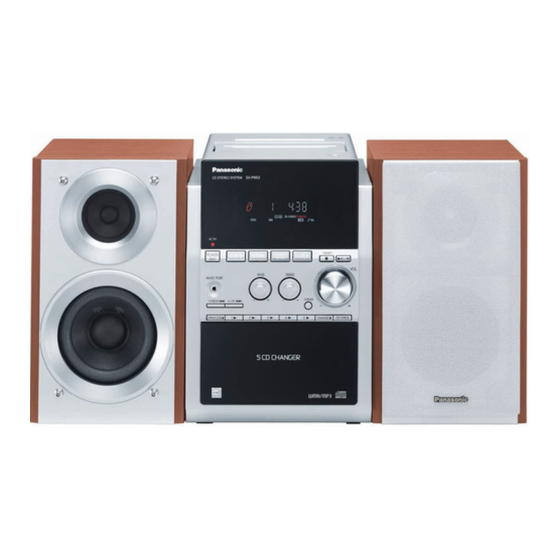
SA-PM53E
SA-PM53EB
SA-PM53EG
Colour
(S)... Silver Type
S/N 20 dB (at 999 kHz)
n Cassette Deck Section
Track system
Heads
Record/playback
Erasure
Motor
Recording system
Erase system
Tape speed
Overall frequency response (+3, -6 dB at DECK OUT)
NORMAL
S/N RATIO
Wow and flutter
Fast forward and rewind time
n CD Section
Disc played [8 cm or 12 cm]
(1) CD-Audio (CD-DA)
(2) CD-R/RW (CD-DA, MP3 formatted disc)
(3) MP3
Sampling frequency
CD
MP3
Bit rate
MP3
© 2006 Matsushita Electric Industrial Co. Ltd.. All
rights
reserved.
distribution is a violation of law.
ORDER NO. MD0602043C2
CD Stereo System
4-track, 2-channel
Solid permalloy head
Double gap ferrite head
DC servo motor
AC bias 100 kHz
AC erase 100 kHz
35 Hz to 14 kHz
54 dB (A weighted)
0.08% (WRMS)
Approx. 120 seconds with C-60
cassette tape
32 kHz, 44.1 kHz, 48 kHz
32 kbps to 384 kbps
Unauthorized
copying
900 µV/m
4.8 cm/s
44.1 kHz
and
Advertisement
Table of Contents

Related Manuals for Panasonic SA-PM53E


Summary of Contents for Panasonic SA-PM53E
-
Page 1: Laser Power Class
ORDER NO. MD0602043C2 CD Stereo System SA-PM53E SA-PM53EB SA-PM53EG Colour (S)... Silver Type Specification n Amplifier Section S/N 20 dB (at 999 kHz) 900 µV/m RMS OUTPUT POWER both channel driven n Cassette Deck Section 10% Total harmonic distortion Track system 4-track, 2-channel 50 W per channel (6 Ω) -
Page 2: Table Of Contents
SA-PM53E / SA-PM53EB / SA-PM53EG Decoding 16/20/24 bit linear Operating temperature range +5°C to +35°C Pickup Operating humidity range 5% to 90% RH (no condensation) Wavelength 785 nm Power consumption in standby 0.6 W mode Beam source Semiconductor laser Notes :... - Page 3 SA-PM53E / SA-PM53EB / SA-PM53EG 10.2. Checking and Repairing of Transformer P.C.B. 17.7. CD LOADING CIRCUIT 10.3. Checking and Repairing of Main P.C.B. 18 Printed Circuit Board Diagrams 10.4. Checking and Repairing of Panel P.C.B. 18.1. CD SERVO P.C.B 10.5. Checking and Repairing of CD Servo and CD Loading 18.2.
-
Page 4: Safety Precautions
SA-PM53E / SA-PM53EB / SA-PM53EG 1 Safety Precautions 1.1. GENERAL GUIDELINES 1. When servicing, observe the original lead dress. If a short circuit is found, replace all parts which have been overheated or damaged by the short circuit. 2. After servicing, ensure that all the protective devices such as insulation barriers, insulation papers shields are properly installed. -
Page 5: Caution For Ac Cord
SA-PM53E / SA-PM53EB / SA-PM53EG 1.2. Caution for AC Cord... -
Page 6: Before Repair And Adjustment
SA-PM53E / SA-PM53EB / SA-PM53EG 1.3. Before Repair and Adjustment Disconnect AC power, discharge Power Supply Capacitors C512, C513, C514, C606, C608, C610, C624 through a 10Ω, 1W resistor to ground. DO NOT SHORT-CIRCUIT DIRECTLY (with a screwdriver blade, for instance), as this may destroy solid state devices. -
Page 7: Prevention Of Electro Static Discharge (Esd) To Electrostatically Sensitive (Es) Devices
SA-PM53E / SA-PM53EB / SA-PM53EG 2 Prevention of Electro Static Discharge (ESD) to Electrostatically Sensitive (ES) Devices Some semiconductor (solid state) devices can be damaged easily by electricity. Such components commonly are called Electrostatically Sensitive (ES) Devices. Examples of typical ES devices are integrated circuits and some field-effect transistors and semiconductor “chip”... -
Page 8: Precaution Of Laser Diode
SA-PM53E / SA-PM53EB / SA-PM53EG 3 Precaution of Laser Diode Caution : This product utilizes a laser diode with the unit turned "ON", invisible laser radiation is emitted from the pick up lens. Wavelength : 780 nm Maximum output radiation power from pick up : 100 µW/VDE Laser radiation from pick up unit is safety level, but be sure the followings: 1. -
Page 9: Handling Precautions For Traverse Deck
SA-PM53E / SA-PM53EB / SA-PM53EG 4 Handling Precautions For Traverse Deck The laser diode in the traverse deck (optical pickup) may break down due to potential difference caused by static electricity of clothes or human body. So, be careful of electrostatic breakdown during repair of the traverse deck (optical pickup). -
Page 10: Handling The Lead-Free Solder
SA-PM53E / SA-PM53EB / SA-PM53EG 5 Handling the Lead-free Solder 5.1. About lead free solder (PbF) Distinction of PbF P.C.B.: P.C.B.s (manufactured) using lead free solder will have a PbF stamp on the P.C.B. Caution: · Pb free solder has a higher melting point than standard solder; Typically the melting point is 50 - 70°F (30 - 40°C) higher. Please use a high temperature soldering iron. -
Page 11: Accessories
SA-PM53E / SA-PM53EB / SA-PM53EG 6 Accessories Note : Refer to Packing Materials & Accessories Parts List (Section 23) for the part number. Remote Control AC Power Cord (For EB) AC Power Cord (For E/EG) AM Loop Antenna FM Antenna... -
Page 12: Operating Instructions Procedures
SA-PM53E / SA-PM53EB / SA-PM53EG 7 Operating Instructions Procedures 7.1. Main Unit & Remote Control Operation... -
Page 13: Disc Information
SA-PM53E / SA-PM53EB / SA-PM53EG 7.2. Disc Information... -
Page 14: Self-Diagnosis & Special Mode Setting
SA-PM53E / SA-PM53EB / SA-PM53EG 8 Self-Diagnosis & Special Mode Setting This unit is equipped with features of self-diagnostic & special mode setting for checking the functions & reliability. Special Note : Checking of the reliability (ageing) & changer operation must be carry out to ensure good working condition in unit. - Page 15 SA-PM53E / SA-PM53EB / SA-PM53EG Item FL Display Key Operation Mode Name Description Front Key Volume Setting To Forced Volume In doctor mode: Setting. 1. Press [7] button on remote control. · BASS TREBLE set to 2. Press [8] button on remote control.
- Page 16 SA-PM53E / SA-PM53EB / SA-PM53EG Operation Procedures Micon operation & processing [TAPE ] Key is pressed, after loading in a TPS operation is executed. Check the following. NORMAL, CrO2, METAL type cassette ( { F.REC INH SW } is ON cassette for TPS checking purposes and with { R.REC INH SW } is ON...
- Page 17 SA-PM53E / SA-PM53EB / SA-PM53EG...
- Page 18 SA-PM53E / SA-PM53EB / SA-PM53EG 8.1.3. EEPROM Checksum (ROM correction) Purpose : To check for micro-processor firmware version & EEPROM check (ROM correction). Below is the procedures for this mode. Step 1: Enter into Doctor mode (For more information refer to section 8.1 on key operation to enter into this mode).
- Page 19 SA-PM53E / SA-PM53EB / SA-PM53EG Step 2: Check for firmware version & EEPROM checksum. · When entering into DOCTOR MODE the firmware version & checksum of EEPROM (if applicable) will appear on FL display. Below is information on the EEPROM IC (Rom correction) under 3 examples: 1.
- Page 20 SA-PM53E / SA-PM53EB / SA-PM53EG Note : When in CD to Tape Recording Test mode, the following process is perform : a) If the erasure prevention tab for FWD side the tape is broken, it is judged as an error and the recording operation does not start.
- Page 21 SA-PM53E / SA-PM53EB / SA-PM53EG 8.1.7. RDS Checking Purpose : To check the RDS Function. Below is the procedures for this mode. Step 1: Enter into Doctor mode (For more information refer to section 8.1 on key operation to enter into this mode).
- Page 22 SA-PM53E / SA-PM53EB / SA-PM53EG 8.1.8. CR 16 Self Diagnostic · In order to improve the analysis of faulty condition in CR16 mechanism, CR16 related error codes have been further divided. Mode Present After modify Description Initialize F17P Play F22L...
-
Page 23: Error Code Table
SA-PM53E / SA-PM53EB / SA-PM53EG error code. 2. To display all error code memorized In "CR16 Self Diagnostic mode", press [CD CHECK] to display subsequence error code. It shall repeat after reaching error no. 5. 3. To clear the error code memory In "CR16 Self Diagnostic mode", long press [CD CHECK] key (2s or more). - Page 24 SA-PM53E / SA-PM53EB / SA-PM53EG Error Code Diagnosis Contents Description of error Automatic FL Display Remarks TPS abnormal For deck mechanism unit (For deck 1/2). Press [ ] on main unit for next error. REST CD traverse position intial For CD unit (For Traverse).
- Page 25 SA-PM53E / SA-PM53EB / SA-PM53EG Error Code Diagnosis Contents Description of error Automatic FL Display Remarks POWER During normal operation, if For Power Supply Related Error AMP output DCDET becomes "L", Detection. abnormal normal POWER OFF Press [ ] on main unit for next process shall not be error.
-
Page 26: Assembling And Disassembling
SA-PM53E / SA-PM53EB / SA-PM53EG 9 Assembling and Disassembling 9.1. Caution “ATTENTION SERVICER” Some chassis components may be have sharp edges. Be careful when disassembling and servicing. 1. This section describes procedures for checking the operation of the major printed circuit boards and replacing the main components. -
Page 27: Disassembly Flow Chart
SA-PM53E / SA-PM53EB / SA-PM53EG 9.2. Disassembly flow chart The following chart is the procedure for disassembling the casing and inside parts for internal inspection when carrying out the servicing. To assemble the unit, reverse the steps shown in the chart below. -
Page 28: Main Parts Location Diagram
SA-PM53E / SA-PM53EB / SA-PM53EG 9.3. Main Parts Location Diagram... -
Page 29: Disassembly Of Side Panel L & R
SA-PM53E / SA-PM53EB / SA-PM53EG 9.4. Disassembly of Side Panel L & · Disassembly of Side Panel (R) Step 1 : Lift up the top cabinet as arrow shown (Be careful of the catches). Step 1 : Remove 5 screws from the side panel (R). -
Page 30: Disassembly Of Front Panel
SA-PM53E / SA-PM53EB / SA-PM53EG Step 1 : Remove 1 screw. Step 1 : Detach the connector CN401 and CN501. Step 2 : Release the clutch and remove the Tape Eject P.C.B.. Step 2 : Remove 1 screw and Chassis ground wire. -
Page 31: Disassembly Of Rear Cabinet
SA-PM53E / SA-PM53EB / SA-PM53EG Step 3 : Remove 8 screws . Step 4 : Release 1 clutch and remove the Panel P.C.B. 9.9. Disassembly of Rear Cabinet · Follow the (Step 1) - (Step 6) of item 9.4. · Follow the (Step 1) - (Step 2) of item 9.5. -
Page 32: Disassembly Of Transformer
SA-PM53E / SA-PM53EB / SA-PM53EG Step 1 : Detach the connector CN401, CN350 and CN351. Step 1 : Detach 2 connectors CN501. Step 2 : Detach the connectors CN200 and CN402 and pull out Step 2 : Remove 4 screws and pull out the Transformer P.C.B. -
Page 33: Disassembly Of Power P.c.b
SA-PM53E / SA-PM53EB / SA-PM53EG Step 1 : Unsolder Z301 and remove the tuner pack as arrow Step 1 : Remove 2 screws. show. 9.13. Disassembly of Power P.C.B. · Follow the (Step 1) - (Step 6) of item 9.4. -
Page 34: Replacement Of Cd Lid
SA-PM53E / SA-PM53EB / SA-PM53EG Step 1 : Remove 2 screws and 2 CD Lid supports. Step 4 : Release the catches and remove the middle block as arrow shown. Step 2 :Release the spring hook as arrow shown. Step 5 : Remove 2 screws and remove the CD Mechanism Unit from the bottom chassis as arrow shown. -
Page 35: Replacement Of Cassette Lid
SA-PM53E / SA-PM53EB / SA-PM53EG Step 3 : Remove the Inner CD Lid as arrow shown. Step 1 : Using screw driver to remove Damper gear as arrow shown. Step 4 : Remove the CD Lid as arrow shown. Step 2 : Remove the cassette open spring as arrows shown in 9.16. -
Page 36: Replacement Of The Power Ic
SA-PM53E / SA-PM53EB / SA-PM53EG Step 1 : Remove 4 screws. Step 2 : Remove 1 screw. Step 3 : Pull both sides cassette holders to the direction of the arrows shown. Step 3 : Unsolder the Power IC501 and 502. -
Page 37: Procedure For Replacing Pinch Roller And Head Block (Deck Mechanism Unit)
SA-PM53E / SA-PM53EB / SA-PM53EG 9.18. Procedure for Replacing Pinch Roller and Head Block (Deck Mechanism Unit) · Follow the (Step 1) - (Step 6) of Item 9.4. · Follow the (Step 1) - (Step 2) of Item 9.5. · Follow the (Step 1) - (Step 4) of Item 9.6. - Page 38 SA-PM53E / SA-PM53EB / SA-PM53EG...
-
Page 39: Procedure For Replacing Parts On Deck Mechanism Pcb
SA-PM53E / SA-PM53EB / SA-PM53EG 9.20. Procedure for Replacing Parts on Deck Mechanism PCB · Follow the (Step 1) - (Step 6) of Item 9.4. · Follow the (Step 1) - (Step 2) of Item 9.5. · Follow the (Step 1) - (Step 4) of Item 9.6. -
Page 40: Replacement Of Optical Pickup Unit (Cd Mechanism)
SA-PM53E / SA-PM53EB / SA-PM53EG 9.22. Replacement of optical pickup unit (CD mechanism) · Follow the (Step 1) - (Step 6) of Item 9.4. · Follow the (Step 1) - (Step 2) of Item 9.5. · Follow the (Step 1) - (Step 4) of Item 9.7. - Page 41 SA-PM53E / SA-PM53EB / SA-PM53EG...
-
Page 42: Replacement Of A Traverse Gear A And A Traverse Gear B
SA-PM53E / SA-PM53EB / SA-PM53EG 9.23. Replacement of a traverse gear A and a traverse gear B · Follow the (Step 1) - (Step 6) of Item 9.4. · Follow the (Step 1) - (Step 2) of Item 9.5. · Follow the (Step 1) - (Step 4) of Item 9.7. -
Page 43: Procedure For Removing Cd Loading Mechanism
SA-PM53E / SA-PM53EB / SA-PM53EG 9.24. Procedure for removing CD loading mechanism 1. Turn off by pressing power SW in the body. 3. Disassemble body, take out CD loading mechanism. 2. Unplug AC power cord after the indication of [GOOD-BYE], then disassemble the body. - Page 44 SA-PM53E / SA-PM53EB / SA-PM53EG 9.25.2. Replacement for the disc tray · Follow the (Step 1) - (Step 6) of Item 9.4. · Follow the (Step 1) - (Step 2) of Item 9.5. · Follow the (Step 1) - (Step 4) of Item 9.7.
- Page 45 SA-PM53E / SA-PM53EB / SA-PM53EG...
- Page 46 SA-PM53E / SA-PM53EB / SA-PM53EG 9.25.3. Replacement for the traverse deck · Follow the (Step 1) - (Step 6) of Item 9.4. · Follow the (Step 1) - (Step 2) of Item 9.5. · Follow the (Step 1) - (Step 4) of Item 9.7.
- Page 47 SA-PM53E / SA-PM53EB / SA-PM53EG...
- Page 48 SA-PM53E / SA-PM53EB / SA-PM53EG...
-
Page 49: Cr16 Mechanism Assembly Procedure
SA-PM53E / SA-PM53EB / SA-PM53EG 9.26. CR16 MECHANISM ASSEMBLY PROCEDURE The following specified greases and/or oil must be applied when some specific parts are changed. 1. Floil grease (VFK1298) : The floil grease must be applied to tray, tray (L) and tray (R). - Page 50 SA-PM53E / SA-PM53EB / SA-PM53EG...
- Page 51 SA-PM53E / SA-PM53EB / SA-PM53EG...
- Page 52 SA-PM53E / SA-PM53EB / SA-PM53EG...
- Page 53 SA-PM53E / SA-PM53EB / SA-PM53EG...
- Page 54 SA-PM53E / SA-PM53EB / SA-PM53EG...
- Page 55 SA-PM53E / SA-PM53EB / SA-PM53EG...
- Page 56 SA-PM53E / SA-PM53EB / SA-PM53EG...
- Page 57 SA-PM53E / SA-PM53EB / SA-PM53EG...
- Page 58 SA-PM53E / SA-PM53EB / SA-PM53EG...
- Page 59 SA-PM53E / SA-PM53EB / SA-PM53EG...
- Page 60 SA-PM53E / SA-PM53EB / SA-PM53EG...
- Page 61 SA-PM53E / SA-PM53EB / SA-PM53EG...
-
Page 62: Disassembly Of Traverse Mechanism
SA-PM53E / SA-PM53EB / SA-PM53EG 9.27. Disassembly of traverse mechanism · Follow the (Step 1) - (Step 6) of Item 9.4. · Follow the (Step 1) - (Step 2) of Item 9.5. · Follow the (Step 1) - (Step 4) of Item 9.7. -
Page 63: Handling Of Cassette Tape Jam
SA-PM53E / SA-PM53EB / SA-PM53EG 9.28. Handling of cassette tape jam · Follow the (Step 1) - (Step 6) of Item 9.4. Step 2 : Push the lever as arrow shown to open the cassette lid and remove the cassette tape. -
Page 64: Service Positions
SA-PM53E / SA-PM53EB / SA-PM53EG 10 Service Positions Note: For description of the disassembly procedures, see the Section 9. 10.1. Checking and Repairing of Deck, Deck Mechanism and Tape Eject P.C.B. -
Page 65: Checking And Repairing Of Transformer P.c.b
SA-PM53E / SA-PM53EB / SA-PM53EG 10.2. Checking and Repairing of Transformer P.C.B. -
Page 66: Checking And Repairing Of Main P.c.b
SA-PM53E / SA-PM53EB / SA-PM53EG 10.3. Checking and Repairing of Main P.C.B. -
Page 67: Checking And Repairing Of Panel
SA-PM53E / SA-PM53EB / SA-PM53EG 10.4. Checking and Repairing of Panel P.C.B. -
Page 68: Checking And Repairing Of Cd Servo And Cd Loading
SA-PM53E / SA-PM53EB / SA-PM53EG 10.5. Checking and Repairing of CD Servo and CD Loading P.C.B. -
Page 69: Checking And Repairing Of Power P.c.b
SA-PM53E / SA-PM53EB / SA-PM53EG 10.6. Checking and Repairing of Power P.C.B. -
Page 70: Procedure For Checking Operation Of Individual Parts Of Deck Mechanism Unit
SA-PM53E / SA-PM53EB / SA-PM53EG 11 Procedure for Checking Operation of Individual Parts of Deck Mechanism Unit 11.1. Operation Check with Cassette Tape 1. Pull up the EJECT lever using a rubber band. (Fig. 6) 2. Supply DC5V to MOTOR. (→ MOTOR rotates.) (Fig. 5) 3. - Page 71 SA-PM53E / SA-PM53EB / SA-PM53EG Fig. 7...
-
Page 72: Measurement And Adjustments
SA-PM53E / SA-PM53EB / SA-PM53EG 12 Measurement And Adjustments 12.1. Cassette Deck Section 12.1.1. Requirements · Test tape (QZZCFM) (QZZCWAT) · Normal blank cassette tape (QZZCRA) · Digital frequency counter · Oscilloscope · Electrical voltmeter · Headphone jack output jig (Fig. 8) 12.1.2. - Page 73 SA-PM53E / SA-PM53EB / SA-PM53EG Fig. 10 Fig. 11 12.1.5. Bias Voltage Check 1. Connect an electrical voltmeter. (Fig. 9) (Fig. 12) 2. Set the function to “TAPE” position. 3. Insert a normal blank cassette tape (QZZCRA). 4. While pressing and holding down [REC ( )] button, press [TAPE ( )] button to pause the recording mode.
-
Page 74: Voltage Measurement & Waveform Chart
SA-PM53E / SA-PM53EB / SA-PM53EG 13 Voltage Measurement & Waveform Chart Note: · Indicated voltage values are the standard values for the unit measured by the DC electronic circuit tester (high-impedance) with the chassis taken as standard. Therefore, there may exist some errors in the voltage values, depending on the internal impedance of the DC circuit tester. - Page 75 SA-PM53E / SA-PM53EB / SA-PM53EG 13.1.3. Main P.C.B. MAIN P.C.B. IC201 Ref No. MODE CD PLAY STANDBY IC401 Ref No. MODE CD PLAY STANDBY Ref No. IC401 MODE CD PLAY STANDBY Ref No. IC401 MODE CD PLAY STANDBY Ref No.
- Page 76 SA-PM53E / SA-PM53EB / SA-PM53EG 13.1.5. Deck P.C.B. DECK P.C.B. IC1000 Ref No. MODE CD PLAY STANDBY Ref No. IC1001 MODE CD PLAY STANDBY IC1001 Ref No. MODE CD PLAY STANDBY Q1101 Q1201 Q1302 Q1303 Q1304 Ref No. MODE CD PLAY STANDBY Ref No.
-
Page 77: Waveform Chart
SA-PM53E / SA-PM53EB / SA-PM53EG 13.2. Waveform Chart CN351 PIN 4 CN351 PIN 5 CN351 PIN 6 CN351 PIN 7 CD PLAY CD PLAY CD PLAY CD PLAY 3.48Vp-p (10msec.div) 3.44Vp-p (10msec.div) 4.04Vp-p (25msec.div) 4.36Vp-p (10msec.div) CN351 PIN 8 CN351 PIN 15... - Page 78 SA-PM53E / SA-PM53EB / SA-PM53EG IC401 PIN 13 IC401 PIN 15 IC401 PIN 19 IC401 PIN 28 CD PLAY CD PLAY CD PLAY CD PLAY 3.76Vp-p (100nsec.div) 2.64Vp-p (100nsec.div) 3.44Vp-p (10msec.div) 4.2Vp-p (10msec.div) IC401 PIN 30 IC401 PIN 39 IC401 PIN 42...
-
Page 79: Wiring Connection Diagram
SA-PM53E / SA-PM53EB / SA-PM53EG 14 Wiring Connection Diagram FAN UNIT AC IN... - Page 80 SA-PM53E / SA-PM53EB / SA-PM53EG...
-
Page 81: Block Diagram
SA-PM53E / SA-PM53EB / SA-PM53EG 15 Block Diagram... - Page 82 SA-PM53E / SA-PM53EB / SA-PM53EG...
- Page 83 SA-PM53E / SA-PM53EB / SA-PM53EG...
- Page 84 SA-PM53E / SA-PM53EB / SA-PM53EG...
-
Page 85: Notes Of Schematic Diagram
SA-PM53E / SA-PM53EB / SA-PM53EG 16 Notes of Schematic Diagram (All schematic diagrams may be modified at any time with the development of new technology) Note : STOCK switch PLAY switch BOTTOM switch OPEN switch CHANGE switch S601 STOP/DEMO switch... - Page 86 SA-PM53E / SA-PM53EB / SA-PM53EG...
-
Page 87: Schematic Diagram
SA-PM53E / SA-PM53EB / SA-PM53EG 17 Schematic Diagram 17.1. CD SERVO CIRCUIT... -
Page 88: Main Circuit
SA-PM53E / SA-PM53EB / SA-PM53EG 17.2. MAIN CIRCUIT SCHEMATIC DIAGRAM - 2 : TAPE PLAYBACK SIGNAL LINE : FM/AM SIGNAL LINE : MAIN SIGNAL LINE : -B SIGNAL LINE MAIN CIRCUIT : CD SIGNAL LINE : TAPE RECORD SIGNAL LINE... - Page 89 SA-PM53E / SA-PM53EB / SA-PM53EG SCHEMATIC DIAGRAM - 3 : +B SIGNAL LINE MAIN CIRCUIT : -B SIGNAL LINE : AUX SIGNAL LINE C355 50V2.2 CD3.3V IC403 C0DBZGC00067 REGULATOR WA424 GND Vstdby IC405 C354 C1BB00000943 RDS IC TEST C323 C427...
-
Page 90: Panel Circuit
SA-PM53E / SA-PM53EB / SA-PM53EG 17.3. PANEL CIRCUIT SCHEMATIC DIAGRAM-4 PANEL CIRCUIT : +B SIGNAL LINE : +B SIGNAL LINE : AUX SIGNAL LINE FL601 C606 50V22 A2BB00000157 FL DISPLAY 5 6 7 8 9 10 11 12 13 14 15 16 17 18 19 20 21 22 23 24 25 26 27 28 29 30 31 32 33 34 35... -
Page 91: Deck Circuit, Deck Mechanism Circuit And Tape Eject Circuit
R1343 3.3K WR1308B R1345 WR1308A Q1316 Q1314 Q1315 2SD09650RA B1GDCFGH0002 B1ACKD000006 SWITCH SWITCH SWITCH SA-PM53E/EG/EB DECK / DECK MECHANISM / TAPE EJECT CIRCUIT S1901 WR1903 TAPE EJECT TAPE EJECT CIRCUIT IC971 R972 R973 IC971 DECK MECHANISM CNB13030R2AU PHOTO INTERUPTOR CIRCUIT... -
Page 92: Power Circuit
SA-PM53E / SA-PM53EB / SA-PM53EG 17.5. POWER CIRCUIT SCHEMATIC DIAGRAM-6 POWER CIRCUIT : -B SIGNAL LINE : +B SIGNAL LINE : MAIN SIGNAL LINE QR522 QR522 B1GBCFJJ0044 DC DETECT SWITCH WB512 IC501 IC501 C5ZAZ0000083 R579 CP502 C559 WB505 JK501 POWER HIC... -
Page 93: Transformer Circuit
SA-PM53E / SA-PM53EB / SA-PM53EG 17.6. TRANSFORMER CIRCUIT SCHEMATIC DIAGRAM-7 POWER CIRCUIT(CN501) ON SCHEMATIC DIAGRAM-6 TRANSFORMER CIRCUIT : -B SIGNAL LINE : +B SIGNAL LINE H501/JW501 1 2 3 4 5 6 D520 R511 B0EAKM000117 R512 DGND HALT PCONT T501 G4CYAYY00077 STYBY3.3V... -
Page 94: Cd Loading Circuit
SA-PM53E / SA-PM53EB / SA-PM53EG 17.7. CD LOADING CIRCUIT SCHEMATIC DIAGRAM-8 CD LOADING CIRCUIT : +B SIGNAL LINE IC11 C0GAG0000007 DRIVER IC 0.01 16V100 RM11 UP/DOWN MOTOR CHANGE BOTTOM OPEN B3NAA0000098 SENSOR +7.5V STOCK PGND CR16 SWITCH DNGD UP/DOWN F... -
Page 95: Printed Circuit Board Diagrams
SA-PM53E / SA-PM53EB / SA-PM53EG 18 Printed Circuit Board Diagrams 18.1. CD SERVO P.C.B CD SERVO P.C.B (REPV0082A) TP51 (RF) C7227 W7014 TP19 C7225 TP14 W7015 C7226 C7204 TP50 C7228 TP17 C7216 C7230 TP18 C7231 TP24 CN7002 W7019 R7221 TP13... -
Page 96: Main P.c.b
SA-PM53E / SA-PM53EB / SA-PM53EG 18.2. MAIN P.C.B MAIN P.C.B (REPV0086B) PHONE JK201 CN300 (TO FAN) L295 D302 R302 R301 R305 R311 R303 Q304 R304 Q302 C304 Q303 W275...E/EB/EG R307 R312 Q301 W303 C327 X461 R324 IC405 R323 WA434 W221... -
Page 97: Panel P.c.b
SA-PM53E / SA-PM53EB / SA-PM53EG 18.3. PANEL P.C.B PANEL P.C.B (REPV0087B...E/EG) (REPV0087C...EB) C608 FL601 C606 10 11 12 13 14 15 16 17 18 19 20 21 22 23 24 25 26 27 28 29 30 31 32 33 34 35... -
Page 98: Deck P.c.b, Deck Mechanism P.c.b And Tape Eject P.c.b
SA-PM53E / SA-PM53EB / SA-PM53EG 18.4. DECK P.C.B, DECK MECHANISM P.C.B and TAPE EJECT P.C.B DECK P.C.B (REPV0016B) DECK MECHANISM P.C.B (REPX0321H) S973 (CR02) WR1308B W1930 Q1309 CN1305 Q1310 R1380 W1909 W1935 S972 C1317 R1331 W1977 S971 (HALF) CS971 C1311... -
Page 99: Power P.c.b
SA-PM53E / SA-PM53EB / SA-PM53EG 18.5. POWER P.C.B POWER P.C.B (REPV0086B) W550 W564 WB518 WB513 W565 W567 CP501 CP502 WB517 WB502 Q524 E502 WB512 WB504 WB519 WB505 W514 W537 W591 R751 Q515 W592 W586 1-LO-L QR522 C555 W519 WB511 R750... -
Page 100: Transformer P.c.b
SA-PM53E / SA-PM53EB / SA-PM53EG 18.6. TRANSFORMER P.C.B TRANSFORMER P.C.B (REPV0087B...E/EG) (REPV0087C...EB) 250V 1A D513 D512 QR503 T502 (SUB -TRANSFORMER) W712 CN501 W708 C512 D511 D510 W714 RL501 W725 W716 IC503 Q502 C509 C507 Q501 W706 T501 (POWER TRANSFORMER) C504... -
Page 101: Cd Loading P.c.b
SA-PM53E / SA-PM53EB / SA-PM53EG 18.7. CD LOADING P.C.B CD LOADING P.C.B (REP3569A) (BOTTOMSW) RM11 IC11 (UPDOWN) (PLAYSW) (CHANGESW) (STOCKSW) RM21 (LOADING_MOTOR) IC21 (OPENSW) 2771A-1 2771A-1... - Page 102 SA-PM53E / SA-PM53EB / SA-PM53EG...
-
Page 103: Illustration Of Ic 痴, Transistors And Diodes
SA-PM53E / SA-PM53EB / SA-PM53EG 19 Illustration of IC's, Transistors and Diodes C0DAZYY00005 MN6627954MA (100P) C2CBYY000164 (100P) C0DBZGC00067 C1AA00000612 (5P) C0DAZYY00006 C1BB00001121 (56P) C0HBB0000057 (44P) C0AABB000125 CNB13030R2AU C5ZAZ0000083 C0GAG0000007 BA5948FPE2 (28P) AN7326K (22P) C1BB00000943 (16P) B1BCCG000002 2SD09650RA B1GDCFJJ0002 B1GBCFLL0037 B1ADCF000001... -
Page 104: Terminal Function Of IcエS
SA-PM53E / SA-PM53EB / SA-PM53EG 20 Terminal Function of IC's 20.1. IC7001 (MN6627954MA) IC SERVO PROCESSOR/DIGITAL SIGNAL PROCESSOR/DIGITAL FILTER D/A CONVERTER Pin No. Mark Function Pin No. Mark Function DRAM address signal O/P 11 IREF Reference I/P DRAM address signal O/P 9... -
Page 105: Ic7002 (Ba5948Fpe2) Ic 4Ch Drive
SA-PM53E / SA-PM53EB / SA-PM53EG 20.2. IC7002 (BA5948FPE2) IC 4CH Drive Pin No. Mark Function Pin No. Mark Function Motor Driver 92 Input Motor Drive (3) reverse - action output Turntable Motor Drive Signal (“L”:ON) Motor Drive (3) forward - action... - Page 106 SA-PM53E / SA-PM53EB / SA-PM53EG Pin No. Mark Function RDS_RDY No Connection N.C. No Connection N.C. No Connection MOTOR MOTOR PLUNGER PLUNGER N.C. No Connection HP_SW HP_SW REST_SW REST_SW CD_RST CD Reset Output N.C. No Connection N.C. No Connection N.C.
-
Page 107: Troubleshooting Flowchart (Cd Section Circuit)
SA-PM53E / SA-PM53EB / SA-PM53EG 21 Troubleshooting Flowchart (CD Section Circuit) - Page 108 SA-PM53E / SA-PM53EB / SA-PM53EG...
-
Page 109: Exploded Views
SA-PM53E / SA-PM53EB / SA-PM53EG 22 Exploded Views 22.1. Cabinet Parts Location... -
Page 110: Cd Loading Mechanism Parts Location
SA-PM53E / SA-PM53EB / SA-PM53EG 22.2. CD Loading Mechanism Parts Location... -
Page 111: Deck Mechanism (Raa4402-1S) & Traverse Parts Location
SA-PM53E / SA-PM53EB / SA-PM53EG 22.3. Deck Mechanism (RAA4402-1S) & Traverse Parts Location... -
Page 112: Packaging
SA-PM53E / SA-PM53EB / SA-PM53EG 22.4. Packaging... -
Page 113: Replacement Parts List
SA-PM53E / SA-PM53EB / SA-PM53EG 23 Replacement Parts List Notes: · Important safety notice: Components identified by mark have special characteristics important for safety. Furthermore, special parts which have purposes of fire-retardent (resistors), high-quality sound (capacitors), low noise (resistors), etc are used. - Page 114 SA-PM53E / SA-PM53EB / SA-PM53EG Ref. Part No. Part Name & Description Remarks Ref. Part No. Part Name & Description Remarks RXQ0470-2 PLUNGER RMR1714A-H TRAY RMC0061 PACK SPRING RMR1714B-H TRAY RXF0061-1 FLYWHEEL F ASS’Y RMR1714C-H TRAY RXG0040 FF RELAY GEAR ASS’Y...
- Page 115 SA-PM53E / SA-PM53EB / SA-PM53EG Ref. Part No. Part Name & Description Remarks Ref. Part No. Part Name & Description Remarks Q301 B1ABCF000079 TRANSISTOR D602 B3AAA0000489 DIODE Q302 B1ABCF000079 TRANSISTOR D971 MA2C16500E DIODE Q303 B1ACKD000006 TRANSISTOR D1301 B0ACCK000005 DIODE Q304...
- Page 116 SA-PM53E / SA-PM53EB / SA-PM53EG Ref. Part No. Part Name & Description Remarks Ref. Part No. Part Name & Description Remarks L292 J0JBC0000019 CHIP INDUCTOR JW501 REXV0065 10P WIRE L295 J0JBC0000019 CHIP INDUCTOR JW601 RWJ0209150XQ 9P WIRE L301 G0A200D00002 RF CHOKE COIL...
- Page 117 SA-PM53E / SA-PM53EB / SA-PM53EG Ref. Part No. Part Name & Description Remarks Ref. Part No. Part Name & Description Remarks R252 D0GB104JA007 100K 1/16W R418 D0GB101JA007 100 1/16W R253 D0GB221JA007 220 1/16W R419 D0GB101JA007 100 1/16W R254 D0GB221JA007 220 1/16W...
- Page 118 SA-PM53E / SA-PM53EB / SA-PM53EG Ref. Part No. Part Name & Description Remarks Ref. Part No. Part Name & Description Remarks R527 D0GB473JA041 47K 1/16W R1061 ERJ3GEY0R00V 0 1/16W R528 D0GB104JA007 100K 1/16W R1063 ERJ3GEY0R00V 0 1/16W R552 ERJ3GEYJ122V 1.2K 1/16W...
- Page 119 SA-PM53E / SA-PM53EB / SA-PM53EG Ref. Part No. Part Name & Description Remarks Ref. Part No. Part Name & Description Remarks R7335 D0GB101JA007 100 1/16W WA642 ERJ3GEY0R00V CHIP JUMPER R7336 D0GB100JA007 10 1/16W WA644 ERJ6GEY0R00V CHIP JUMPER R7339 ERJ3GEYJ102V 1K 1/16W...
- Page 120 SA-PM53E / SA-PM53EB / SA-PM53EG Ref. Part No. Part Name & Description Remarks Ref. Part No. Part Name & Description Remarks C236 F1H1C104A041 0.1 16V C413 ECJ1VC1H220J 22P 50V C237 F1H1H221A748 220P 50V C414 ECJ1VC1H101K 100P 50V C238 F1H1H221A748 220P 50V...
- Page 121 SA-PM53E / SA-PM53EB / SA-PM53EG Ref. Part No. Part Name & Description Remarks Ref. Part No. Part Name & Description Remarks C621 F1H1H221A748 220P 50V C1371 F1H1E103A029 0.01 25V C622 F1H1H221A748 220P 50V C7102 ECJ1VB1A474K 0.47 10V C623 F1H1H221A748 220P 50V...
Need help?
Do you have a question about the SA-PM53E and is the answer not in the manual?
Questions and answers