Table of Contents
Advertisement
Quick Links
Specifications
Power Source :
Power Consumption :
Aerial Impedance :
Receiving Channels :
VHF
CATV
UHF
Intermediate Frequency :
Video
Sound
Colour
AC AUTO 110-240V, 50/60 Hz
83W
75Ω unbalanced
Coaxial type
2-13 (USA STANDARD)
1-125 (USA STANDARD)
14-69 (USA STANDARD)
38.0 MHz
31.5 MHz (D, K, K1)
32 MHz (I)
32.5 MHz (B, G)
33.5 MHz (M)
33.57 MHz (PAL)
33.6 MHz (SECAM)
33.75 MHz (SECAM)
34.42 MHz (NTSC)
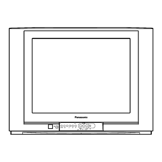
TC-21FG10P
GP31 Chassis
Video / Terminals :
RAV In
Monitor Out
High Voltage :
Picture Tube :
Audio Output :
Dimensions :
Mass :
Specifications are subject to change without notice.
Mass and dimensions shown are approximate.
© 2005 Matsushita Electric Industrial Co., Ltd. All
rights
reserved.
distribution is a violation of law.
ORDER NO. MTV0501395C3
Colour Television
AV1, 2
Video In 1 Vp-p 75Ω
Audio In Approx. 400mVrms
Video Out 1 Vp-p 75Ω
Audio Out Approx. 400mVrms
27.5kV±1.5
at zero beam current
A51LXR195X
51cm (21 inches)
Measured diagonally,
90° deflection
16.0W
Height : 473 mm
Width : 648 mm
Depth : 488 mm
24 kg (Net Wt.)
Unauthorized
copying
and
Advertisement
Table of Contents

Subscribe to Our Youtube Channel
Related Manuals for Panasonic TC-21FG10P


Summary of Contents for Panasonic TC-21FG10P
-
Page 1: Colour Television
ORDER NO. MTV0501395C3 Colour Television TC-21FG10P GP31 Chassis Specifications Power Source : AC AUTO 110-240V, 50/60 Hz Video / Terminals : AV1, 2 Power Consumption : RAV In Video In 1 Vp-p 75Ω Aerial Impedance : 75Ω unbalanced Audio In Approx. 400mVrms... -
Page 2: Table Of Contents
CONTENTS Page Page 1 Safety Precautions 2.5. Adjustment Procedure 1.1. General Guide Lines 2.6. PAL Colour 1.2. Leakage Current Cold Check 2.7. Adjustment 1.3. Leakage Current Hot Check (Fig. 1) 3 Conductor Views 1.4. X-Radiation 4 Schematic Diagram 1.5. GP31 Chassis Block Diagram 4.1. -
Page 3: Safety Precautions
1 Safety Precautions 1.1. General Guide Lines 1. It is advisable to insert an isolation transformer in the AC supply before servicing this hot chassis. 2. When servicing, observe the original lead dress, especially the lead dress in the high voltage circuits. If a short circuit is found, replace all parts which have been overheated or damaged by the short circuit. -
Page 4: Gp31 Chassis Block Diagram
1.5. GP31 Chassis Block Diagram... -
Page 5: Service Hints
2 Service Hints 2.1. Service Position for E-Board 1. Remove the back cover. 2. Stand the TV set as shown in Fig. 2. 3. Remove the A-Board from the TV set by pulling the main board out as shown in Figure 2. Fig. -
Page 6: Adjustment For White Balance
2.3. Adjustment for White Balance Preparation: 1. Receive the white balance pattern and aging should have been performed over 30 minutes. 2. Set the picture menu to DYNAMIC NORMAL. 3. Degausse the CRT face. 4. Fix the CRT colour analyzer receiver unit to CRT face. Adjustment of Low Light. -
Page 7: Adjustment Procedure
2.5. Adjustment Procedure 2.5.1. +B Voltage 2.5.3. High Voltage Item / preparation Item / preparation 1. Operate the TV set. 1. Receive the crosshatch pattern. 2. Set control as follows : 2. Set to 0 Beam. Brightness ... minimum Screen VR ..minimum Contrast .... -
Page 8: Pal Colour
2.6. PAL Colour 1. Receive the PAL B/G studio colour bar pattern and adjust local frequency at the best tuned position. 2. Pic Menu: Dynamic Normal, Confirm Contrast - 100 DAC, Sub Contrast - 21 dac. 3. Channel colour set --------- STD 4. - Page 9 Before Colour Purity, Convergence and White Balance adjustment are attempted, V. Height, H. Centre and Focus adjustments must be completed. Colour Purity Convergence 1. Set the Brightness and Contrast controls to their maximum 1. Apply a crosshatch pattern signal and Normalize Contrast positions.
- Page 10 Adjustment of CRT VRS 1. Preparation a. Set DY to CRT not to tilt up and down left and right deflection. b. Set CY to CRT and set CY magnet primarily (Fig. 1) Purity magnet : Set purity magnet that 2 magnets are (TOP POSITION) VRS magnet : Set purity magnet 2 magnets are (HORIZONTAL POSITION) 2.
- Page 11 Fig. 10 Fig. 11 Notes: 1. Wedge A, B and C should be inserted following the sequence of 1, 2 and 3 shown in Fig. 11. 2. The wedges should be set 120° apart from each other. 3. Be certain that three wedges are firmly fixed and the Deflection Yoke is tightly clamped in place. Otherwise the Deflection Yoke may shift its position and cause a loss of convergence and purity.
-
Page 12: Conductor Views
3 Conductor Views... -
Page 13: Schematic Diagram
4 Schematic Diagram... -
Page 15: A Board
4.1. A Board 4.1.1. A Board (1/5) <1A> <2A> <3A> <4A> <5A> <6A> <7A> <8A>... - Page 16 4.1.2. A Board (2/5) <1A> <1B> <2B> <2A> <3B> <3A> <4A> <4B> <5A> <5B> <6A> <6B> <7B> <7A> <8A> <8B>...
- Page 17 4.1.3. A Board (3/5) <1B> <1C> <2B> <2C> <3C> <3B> <4C> <5C> <4B> <5B> <6C> <6B> <7B> <7C> <8B> <8C>...
- Page 18 4.1.4. A Board (4/5) <1C> <1D> <2D> <2C> <3C> <3D> <4D> <4C> <5C> <5D> <6C> <6D> <7D> <7C> <8C>...
- Page 19 4.1.5. A Board (5/5) <1D> <2D> <3D> <4D> <5D> <6D> <7D>...
-
Page 20: L Board
4.2. L Board 4.2.1. L Board (1/3) <1A> <2A> <3A> <4A> <5A> <6A>... - Page 21 4.2.2. L Board (2/3) <1A> <1B> <2A> <3A> <2B> <4A> <5A> <3B> <4B> <5B> <6A> <6B>...
- Page 22 4.2.3. L Board (3/3) <1B> <2B> <3B> <4B> <5B> <6B>...
-
Page 23: Parts Locations
5 Parts Locations... -
Page 24: Replacement Parts List
6 Replacement Parts List... -
Page 25: Replacement Parts List
C 1000PF, K, 2KV K2JZ2B000021 ANTENNA PLUG C371 ECEA1CN100U E 10UF, 16V TBM4G1238 MODEL NAME PLATE C373 ECA2EM100B E 10UF, 250V TBM4G3013 PANASONIC BADGE C377 ECA1CM221B E 220UF, 16V TBX4G90411 POWER BUTTON C402 ECA1VM101B E 100UF, 35V TES4G206 COIL SPRING C404 ECQB1333JF P 0.033UF, J,100V... - Page 26 Ref. Part No. Part Name & Description Remarks Ref. Part No. Part Name & Description Remarks C689 ECJ2VF1H104Z C 0.1UF, Z, 50V D552 B0HAJP000015 DIODE C801 ECQU2A224BN9 P 0.22UF, 250V D555 B0ACQJ000001 DIODE C802 ECQU2A224BN9 P 0.22UF, 250V D556 ERB06-15 DIODE C806 ECKWAE472ZED...
- Page 27 Ref. Part No. Part Name & Description Remarks Ref. Part No. Part Name & Description Remarks Q2381 B1ADDF000005 TRANSISTOR R2120 D0GD103JA017 D0GD103JA017 Q3030 B1ABCE000015 TRANSISTOR R2121 D0GD683JA017 F 68KOHM,J, 1/10W Q3031 B1ABCE000015 TRANSISTOR R2122 D0GD683JA017 F 68KOHM,J, 1/10W Q3150 B1ABCE000015 TRANSISTOR R2302 D0GD153JA017...
- Page 28 Ref. Part No. Part Name & Description Remarks Ref. Part No. Part Name & Description Remarks R560 ERG1SJ102E M 1KOHM,J, 1W JA10 ERJ6GEY0R00 M 0OHM,J,1/10W R563 ERJ6GEY0R00 M 0OHM,J,1/10W JA11 ERJ6GEY0R00 M 0OHM,J,1/10W R564 ERDS2TJ393 C 39KOHM,J, 1/4W JA12 ERJ6GEY0R00 M 0OHM,J,1/10W R580 D0GD392JA017...
Need help?
Do you have a question about the TC-21FG10P and is the answer not in the manual?
Questions and answers