
Related Manuals for PV Electronics Nixie FunKlock


Summary of Contents for PV Electronics Nixie FunKlock
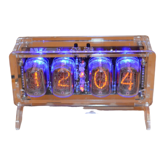
- Page 1 Assembly Instructions User Guide Nixie FunKlock For Parts Bags Serial Numbers 4000 onwards ‘FunKlock’ - 1 - Issue 5 (14 November 2019) www.pvelectronics.co.uk...
- Page 2 REVISION HISTORY Issue Date Reason for Issue Number 14 Nov 2019 Added support for DekaDuo and 3 way header to PCB 1 February 2017 New diode for D2 27 December 2013 C7 / C8 error page 15 7 November 2013 Errors corrected 1 November 2013 New document...
- Page 3 RODUCTION 1. INT Nixie FunKlock - Features - Hours, Minutes and Seconds display on four IN-12 Nixie Tubes - Uses a Quartz Crystal Oscillator as the timebase - Programmable leading zero blanking - Supercapacitor backup. Keeps time during short power outages...
- Page 4 SAFETY DANGER: The clock pcb includes a switched-mode voltage booster circuit. This generates nominally 170 Volts DC, but is capable of generating up to 300 Volts before adjustment. Assembly may only be undertaken by individuals who are suitably qualified and experienced in electronics assembly, and are familiar with safe procedures for working with high voltages.
- Page 5 2. TOOLS AND EQUIPMENT REQUIRED Tools required to assemble the PCB. The following tools will be required to assemble the PCB: Soldering iron with a small tip (1-2 mm) Wire cutters (TIP: A small pair of nail clippers works very well for this function) Wire strippers (TIP: A small pair of scissors is quite suitable) Multimeter for voltage tests and for identifying the resistors.
- Page 6 3. LIST OF COMPONENTS Table of Electronic Components Circuit Designation Part Description Resistors 4.7K, ¼ Watt 390K, ¼ Watt R3, R4, R5 4.7K, ¼ Watt R6 - R9 1K or 1.1K, ¼ Watt R10 - R13 2.7K, ¼ Watt R14, R15 4.7K, ¼...
- Page 7 Electronic Components Parts List / Packing Sheet Part Description Quantity Resistors 270R, ¼ Watt 1K or 1.1K, ¼ Watt 2.7K, ¼ Watt 4.7K, ¼ Watt 390K, ¼ Watt Capacitors 220uF, 16-25V, Electrolytic 1uF 250V, Electrolytic 100nF Ceramic 15pF Ceramic 33pF Ceramic 0.1F or 0.22F Transistors IRFD220 MOSFET...
- Page 8 alarmed if there are some extra components, as some component alarmed if there are some extra components, as some component alarmed if there are some extra components, as some component bags are shared between different kit types. bags are shared between different kit types. The resistors used in the kit are 1% tolerance metal film.
- Page 9 ASSEMBLY OF THE PCB The PCB is supplied as a single board, with a V-score to break in half. Simply bend at the score line and the PCB will split into two parts. Start work below on the tube board: 1mm Sockets For Nixie Tubes There are 44 individual sockets that need to be placed.
- Page 10 Low Voltage Power components: J1, FUSE, D1, D3 (1N5819) D2 (1N4001) IC1 (78L05) C1, C2 (100 nF) Start by installing D1-D3. Align the white band on the components with the band marked on the PCB. Continue to mount C1, C2, J1, IC1 and FUSE. Note that J1, the DC power socket, is mounted on the opposite side of the PCB to the other components.
- Page 11 Plug in the power supply, and then test us Plug in the power supply, and then test using a DC voltmeter: ing a DC voltmeter: Touch the black probe on the GND test point and the red probe on Touch the black probe on the GND test point and the red probe on Touch the black probe on the GND test point and the red probe on the 5V test point.
- Page 12 C3 and C4 are polarised so must be inserted the right way round. The white stripe on the body of the component must be next to the corresponding white marking on ‘FunKlock’ - 12 - Issue 5 (14 November 2019) www.pvelectronics.co.uk...
- Page 13 High Voltage Generator Test. - Refer to the warnings on page 4 - Insert IC2 into its socket. Orient the notch on the IC with the notch on the IC socket and the PCB marking. - Power up the PCB, and using the GND and 170V test points, measure the high voltage generated.
- Page 14 Anode Driver Components Q2 - Q5 (EL817) R6 - R9 (1 KΩ or 1.1 KΩ) R10 - R13 (2.7 KΩ) Assembly now continues on the tube PCB: Orient the dot on the EL817 each optocoupler with the corresponding PCB mark. Board Connectors J2, J5 (10-Way female connector) J3, J4 (10-Way male connector)
- Page 15 Be sure the 'NX4' and 'J4' component markings are at the same side of the stack, or else your tubes will be upside down! Ensure the two PCBs are perfectly square and true, and then solder all the connectors in place. It is a good idea to solder the four top corner pins in place and then the four bottom corner pins first, so the connectors are anchored.
- Page 16 4.10 D5 - D8 (3mm Coloured LED) The LONG lead goes in the hole marked '+'. Put each LED loosely into its holes, and then place the tube PCB into position. Now you can push each LED into the matching small hole in the tube PCB. Turn the PCBs over so you can solder the LEDs in place, ensuring they are pushed completely into the holes in the tube PCB.
- Page 17 4.13 R16, R17 (390 KΩ) AM, PM (4mm neons) Use small pieces of the clear insulation provided, on the leads of the 2 neons to prevent shorts. You can make a test fit of the IN-12 tubes to help you decide the best height from the PCB for them. The insulation is actually heat-shrinkable, so for a very neat finish you can gently blow with hot air to shrink the insulation after soldering the neons in place.
- Page 18 HOW TO OPERATE THE CLOCK The two buttons have the following functions: SET: Set time. Enter configuration menu. ADJ: Adjust time. Adjust configuration values. Entering configuration mode: The principal settings of the clock are stored in flash memory – your preferred configuration is stored even after powering off the clock for extended periods.
- Page 19 Parameter Description Values Software revision 10 = version 1.0, 11 = version 1.1 etc 12 / 24 Hr mode 0 – 12 Hr (default) 1 – 24 Hr Leading zero blanking 0 – leading zero blanked (default) eg. 01:54:32 1 – leading zero displayed Night Mode start hour 0 - 23 Night Mode end hour...
- Page 20 5. Set this parameter to ‘1’ to restore original default settings. Internal operations will then load all the original settings and restore the value to ‘0’ ‘FunKlock’ - 20 - Issue 5 (14 November 2019) www.pvelectronics.co.uk...
- Page 21 Setting the Time: From time display mode, press and hold ‘SET’ button for 2 seconds until the seconds digits are displayed Press the ‘ADJ’ button to reset seconds to zero. Briefly Press ‘SET’ again and the minutes will be highlighted Press the ‘ADJ’...
- Page 22 CONNECTING OUR DEKATRON DRIVER The clock can be connected by just 3 wires to our DekaDuo Dual OG4 Dekatron Driver. Solder the 3 way header as shown below. Control of the Dekatron in night modes is possible using parameter ‘FunKlock’ - 22 - Issue 5 (14 November 2019) www.pvelectronics.co.uk...
- Page 23 ‘FunKlock’ - 23 - Issue 5 (14 November 2019) www.pvelectronics.co.uk...
- Page 24 CIRCUIT DIAGRAM ‘FunKlock’ - 24 - Issue 5 (14 November 2019) www.pvelectronics.co.uk...
- Page 25 ‘FunKlock’ - 25 - Issue 5 (14 November 2019) www.pvelectronics.co.uk...
Need help?
Do you have a question about the Nixie FunKlock and is the answer not in the manual?
Questions and answers