Panasonic EB-G60 Service Manual
Personal cellular telephone
Hide thumbs
Also See for EB-G60:
- Operating instructions manual (117 pages) ,
- Operating instructions manual (126 pages)
Table of Contents
Advertisement
Quick Links
This service information is designed for experienced repair technicians only and is not designed for use by the general public.
It does not contain warnings or cautions to advise non-technical individuals of potential dangers in attempting to service a
product.
Products powered by electricity should be serviced or repaired only by experienced professional technicians. Any attempt to
service or repair the product or products dealt with in this service information by anyone else could result in serious injury or
death.
EB-G60
Y WARNING
R
Personal Cellular Telephone
Frequency Range
Tx/Rx frequency separation
RF Channel Bandwidth
Number of RF channels
Speech coding
Operating temperature
Type
RF Output Power
Modulation
Connection
Transmission speed
Signal Reception
Antenna Impedance
Antenna VSWR
Dimensions
Volume
Weight
Display
Illumination
Keys
SIM
External DC Supply Voltage
Battery
Standby Time
Talk Time
ç 2 0 0 3
P a n a s o n i c M o b i l e C o m m u n i c a t i o n s C o . , L t d .
A l l r i g h t s r e s e r v e d . U n a u t h o r i z e d c o p y i n g a n d
d i s t r i b u t i o n i s a v i o l a t i o n o f l a w .
ORDER NO. OMTD030301C8
900 MHz
1800 MHz
Tx: 880-915 MHz
Tx: 1710-1785 MHz
Rx: 925-960 MHz
Rx: 1805-1880 MHz
45 MHz
95 MHz
200 KHz
174
374
Full rate/Half rate/Enhanced Full rate
–10 °C to +55 °C
Class 4 Handheld
Class 1 Handheld
2W maximum
1W maximum
GMSK (BT = 0.3)
8ch/TDMA
270.833 kbps
Direct conversion
50 Ω
< 3 : 1
104 mm X 47 mm X 19.15 mm
75 cc
84 g
128 X 128 pixels, 4096-colour palette (RGB)
8 LEDs for keypad backlighting (Green)
2 LEDs for LCD backlighting (White)
16-key Keypad, 4-key Direction key,
Navigation key
3 V Plug-in type only
5.8 V
3.7V nominal, 740mAh, Li-lon
100 – 200 hrs maximum
> 180 minutes maximum
Advertisement
Table of Contents

Related Manuals for Panasonic EB-G60


Summary of Contents for Panasonic EB-G60
- Page 1 ORDER NO. OMTD030301C8 Personal Cellular Telephone EB-G60 900 MHz 1800 MHz Frequency Range Tx: 880-915 MHz Tx: 1710-1785 MHz Rx: 925-960 MHz Rx: 1805-1880 MHz Tx/Rx frequency separation 45 MHz 95 MHz RF Channel Bandwidth 200 KHz Number of RF channels...
-
Page 2: Table Of Contents
The information contained in this manual and all rights in any design disclosed therein, are and remain the exclusive property of Panasonic Mobile Communications Co., Ltd. Other patents applying to material contained in this publication:... - Page 3 5.3.3. Functional Description ............. . .5-11 5.4.
- Page 4 9. REPLACEMENT PARTS LIST ..............9-1 9.1.
-
Page 5: Introduction
They must not be incinerated, or disposed of as ordinary rubbish. 1.1. Purpose of the Manual This Service manual contains the information and procedures required for installing, operating and servicing the Panasonic GSM Personal Cellular Mobile Telephone system operating on GSM Digital Cellular Networks. -
Page 6: General Description
2.2. Features The Panasonic Telephone Model G60 is a high performance, small, light, handset for business and domestic use. The following features are provided: Triple Rate, which includes Full Rate, Half rate and Enhanced Full Rate (EFR) speech, codec. -
Page 7: Operating Instructions
3. OPERATING INSTRUCTIONS 3.1. General This section provides a brief guide to the operation and facilities available on the telephone handset. Refer to the Operating Instructions supplied with the telephone for full operational information. 3.2. Liquid Crystal Display The telephone handset has a graphical chip on glass display. The following icons are available: Figure 3.1: Liquid Crystal Display Indicates received signal strength: strong signal area ;... -
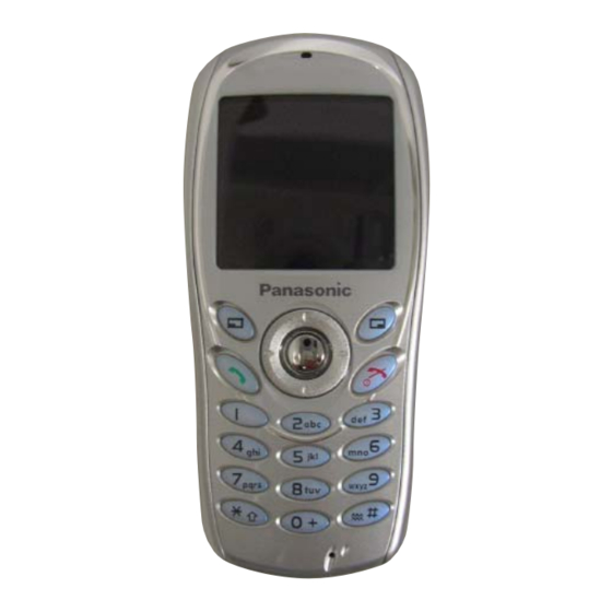
Page 8: Location Of Controls
3.3. Location of Controls Incoming / Charge indicator: Green - Incoming call. Red - Charging battery pack. External connector: Used to connect to external accessories or to charging equipment Receiver Earphone / Microphone Socket Display Navigation Key Microphone External Connector Figure 3.2: Location of Controls The keypad Type A Navigation Key. - Page 9 The keypad Type B Navigation Key. Scrolls through options or features menu and increases or decreases volume. Cancel Key. Used mainly to cancel the current operation and return to the previous menu level. In some menus it has other functions. Option key.
-
Page 10: Alpha Entry
3.4. Alpha Entry 3.4.1 Character Set / Key Assignments Alpha entry is used to enter alphanumeric characters in to the Phonebook, Short Messages and Greeting Message areas The keypad of Type A Character / Operation T9® Normal Greek Extended Numeric Alternatives + –... -
Page 11: Editing Alpha Entry
The keypad of Type B Character / Operation Normal Greek Extended Numeric Alternatives + - 0+P_ Punctuation “ @ – , . ; : ! i ? ¿ ( ) ‘ & % + – / < > = £ $ ¥ ¤ § Α... -
Page 12: Features Menu Structure / Main Menu Options
3.5. Features Menu Structure My Phone Media Folder Picture Melody Sound Setting General Mode Animation Meeting Mode Status Outdoor Mode Display Setting Idle Screen Fixed Data Car Mode User Data Quick Notice Screen Saver Party Mode Language Colour Themes Customized Mode Auto Answer Greeting Default... -
Page 13: Glossary Of Terms
3.6. Glossary of Terms Term Definition DTMF Dual Tone Multiple Frequency tones. The numeric keys 0 to 9, and * and # will generate different DTMF tones when pressed during conversation. These are used to access voice mail, paging and home banking services. Global System for Mobile communications. -
Page 14: Technical Specifications
4. TECHNICAL SPECIFICATIONS 4.1. Tx Characteristics All data is applicable to E-GSM 900 and GSM 1800 except where stated. 4.1.1. Frequency Error ±0.1 ppm max., relative to base station frequency. 4.1.2 Modulation Phase Error RMS: Equal to or less than 5 ° Peak: Equal to or less than 20 °... -
Page 15: Spurious Emissions At Antenna Connector
4.1.5. Spurious Emissions at Antenna Connector Frequency Filter Approx Limits(dBm) Frequency Range offset Bandwidth Video B/W E-GSM 900 GSM1800 10KHz 30KHz 100KHz to 50MHz 100KHz 300KHz 50 to 500MHz 100KHz 300KHz 500MHz to 1GHz 0 to 1MHz 1 GHz to 12.75 GHz 0 to 10MHz 100KHz 300KHz... - Page 16 E-GSM 900 Half Rate Speech The reference sensitivity performance in terms of frame erasure, bit error, or residual bit error rates (whichever is appropriate) is specified in the following table, according to the propagation conditions. Propagation Propagation Propagation Channels conditions conditions conditions TU high...
- Page 17 Blocking: Small MS level in dBµVemf( ) Frequency E-GSM 900 GSM 1800 FR ± 600 kHz to FR ± 800 kHz FR ± 800 kHz to FR± 1,6 MHz FR ± 1,6 MHz to FR ± 3 MHz 915 MHz to FR - 3 MHz FR ±...
-
Page 18: Technical Description
5. TECHNICAL DESCRIPTION 5.1. RF Overview 5.1.1. Introduction General Specifications The telephone is a Dual Band product incorporating two switch able transceivers, one for the E-GSM 900 band and another for the GSM 1800 (DCS 1800) band. The transmit and receive bands for the mobile are given in the table below: E-GSM 900 880 - 915 MHz... -
Page 19: Rf Function Block
5.1.2. RF Function Block Figure 5.1. : RF Function Block Diagram – 5–2 –... -
Page 20: Functional Description
5.1.3. Functional Description Frequency Plan The frequency plan is shown below: TXIF TX UHF LO E-GSM 900 880 - 915 MHz 88.46 - 114.35 MHz 1459.59 - 1543.725 MHz GSM 1800 1710 - 1785 MHz 90.31 - 104.77 MHz 1354.73 - 1414.482 MHz GSM 850 824 - 850 MHz 82.42 - 105.55 MHz... - Page 21 The CX74017 transmitter functional block diagram is shown in Figure 5.2 The transmit (Tx) chain is based on a translational loop architecture. The baseband information is injected within the loop therefore the output signal is phase- modulate. One of the advantages of this architecture is that the Transmit Intermediate Frequency (TxIF) is kept within a narrow frequency range.
-
Page 22: Transmitter
5.2. TRANSMITTER 5.2.1. Introduction This section provides a technical description of the transmitter circuits of the Main PCB. A circuit diagram of the whole system is provided in the Service Manual. 5.2.2. Uplink Frequencies E-GSM 900 The uplink frequencies for the E-GSM 900 band are as follows: CHANNEL UPLINK FREQUENCIES NUMBERS... - Page 23 Uplink frequencies for the standard GSM 900 band (0 = ARFCN = 124) can be calculated as follows: Uplink frequency = 890 MHz + (ARFCN x 0.2 MHz) e.g. for CH55 890 MHz + (55 x 0.2 MHz) = 890 MHz + (11 MHz) = 901 MHz GSM 1800 Uplink frequencies for the GSM 1800 band can be calculated as follows:...
-
Page 24: Functional Description
5.2.3. Functional Description Txin Txqn Txip Txqp TxGSM TxGSM Dual-band ÖÖ . Ö Tx-VCO TxDCS TxDCS UHF-VCO Fref Controller Dual-band (LO) TR switch VCTCXO PA module 13MHz RF3140 Transceiver U106 U104 CX74017 PCO1 PCO2 TXENA Data RXENA U111 SXENA VC1 VC2 VC3 Rxin Rxip Rxqn... - Page 25 The CX74017 transceiver is a highly integrated device for multi-band Global System for Mobile Communications™ (GSM ™) or General Packet Radio Service (GPRS) applications. The device requires a minimal number of external components to complete a GSM radio subsystem. The CX74017 supports EGSM900/DCS1800 applications. The receive path implements a direct down-conversion architecture that eliminates the need for Intermediate Frequency (IF) components.
-
Page 26: Receiver
5.3. RECEIVER 5.3.1. Introduction This Section provides a technical description of the receiver section of the RF circuit. A complete circuit diagram is provided in the Service Manual. 5.3.2. Downlink Frequencies E-GSM 900 The downlink frequencies for the E-GSM 900 band are as follows: CHANNEL DOWNLINK FREQUENCIES NUMBERS... - Page 27 Uplink frequencies for the standard GSM 900 band (0 = ARFCN = 124) can be calculated as follows: Uplink frequency = 935 MHz + (ARFCN x 0.2 MHz) e.g. for CH55 935 MHz + (55 x 0.2 MHz) = 935 MHz + (11 MHz) = 946 MHz GSM 1800 Uplink frequencies for the GSM 1800 band can be calculated as follows:...
-
Page 28: Functional Description
GSM 1900 Uplink frequencies for the GSM 1900 band (512 = ARFCN = 810) can be calculated as follows: Uplink frequency = 1930 MHz + ((ARFCN - 511) x 0.2 MHz) e.g. for CH680 1930 MHz + ((185 - 511) x 0. 2MHz) = 1930 MHz + (33.8 MHz) = 1963.8 MHz 5.3.3. -
Page 29: Baseband Overview
5.4. BASEBAND OVERVIEW 5.4.1. Introduction The baseband circuits of the phone are required to perform the following functions: 8 Equalization 8 Channel coding / decoding 8 Speech coding / decoding 8 Data Encryption 8 Layer 1, 2 and 3 software tasks 8 Man Machine interface (MMI) 8 System Interface 8 SIM Interface and Management... -
Page 30: Keypad
5.5. Keypad The Keypad has a 4 x 5 matrix, allowing 20 keys to be scanned. When a key being pressed, a keypad interrupt is generated. To find which key has been pressed, the software scans each column in turn and reads which row is active. Because of key bounce, the key press is confirmed twice at approximately 20 ms intervals. -
Page 31: Tpu
5.7. TPU The TPU provides the GSM TPU TDMA timing requirements for the system. External timing signals are provided that an area of micro-code. TPU Timing output signal assignments of G2 Name PIN No. Function Connection Configuration TSPACT 0 TXON1 TSPACT 1 TSPACT 2 TSPACT 3... -
Page 32: Lcd
5.9. LCD The LCD module consists of a LCD glass and driver chip connection to the Main PCB via a flexible PCB strip. A 128 x RGB x 128 pixels graphical display is used which can display up to 16 characters x 6 rows-plus two rows of icons. -
Page 33: Microphone
5.11. Microphone The microphone is a noise canceling type to provide improved speech pick-up, noise immunity and reduced echo. The GSM Standard requires that when in handheld mode, the transmitter audio frequency response must fit within the mask shown below: 5.12. -
Page 34: Handfree Mode
5.12.2. Handfree Mode A second speaker is mounted in the rear case for speaker operation. Ring tones and melodies are played via the speaker. The volume level of ring and melody tones are defined YMU759, and the voice volume is defined IOTA. Timer 1 in G2 is used to time the period between switching the ringing on and off to make the tone. -
Page 35: Power Supplies
5.15. POWER SUPPLIES 5.15.1. Introduction – 5–18 –... -
Page 36: Power Source
The Power Management Block consists of six parts as follows: 1. Power Source 2. Power On/Off Control 3. Power Source Failure detection 4. Voltage Regulation 5. Battery Charging & Monitoring 6. Accessory Control 5.15.2. Power Source The battery comprises a single Lithium-Ion (Li-Ion) cell with a nominal voltage of 3.7 V and 780 mAh capacities. This type of battery has an advantage in weight and size over Nickel Metal Hydride (Ni-MH) cells. -
Page 37: Voltage Reguration
5.15.4. Voltage Regulation Each power source is specified as follows. VRDBB: Power supply for G2 Voltage 1.5 V Current 120 mA max Dropout 100 mV max (load max) VRRAM: Power supply for SRAM and G2 Voltage 2.8 V Current 50 mA max Dropout 100 mV max (load max) VRMEM: Power supply for flash memory, LCD and G2... -
Page 38: Deeply Discharged Batteries
The phone will be power down two minutes after generating a Low battery Alarm. Battery charging is controlled by the CPU within the phone. If external power is detected and the temperature is within specified limits, the charger starts the rapid charge algorithm. When the battery is fitted, the charging algorithm is determined by constant voltage and constant current control with time, temperature and voltage safeguards. -
Page 39: Disassemby / Reassemby Instructions
6. DISASSEMBLY / REASSEMBLY INSTRUCTIONS 6.1. General This section provides disassembly and reassembly procedures for the main components of the telephone. These assemblies MUST be performed by qualified service personnel at an authorised service centre. The following Warnings and Cautions MUST be observed during all disassembly / reassembly operations: WARNING The equipment described in this manual contains polarised capacitors utilising liquid electrolyte. - Page 40 Push the battery hook away from the handset and lift out the battery cover. The battery may now be removed from the back of the handset. Use the T5 screwdriver to remove the four case screws located inside the battery compartment. Carefully prise apart the case and cover, creating a gep at the base I/O connector.
- Page 41 Separate by gently twisting the case and cover. Use the T5 screwdriver to remove the two antenna screws located outside the antenna box. Lift the internal antenna assembly from the PCB assembly. – 6–3 –...
- Page 42 Lift the PCB assembly from the upper case. Remove the keypad from the upper case. Remove the microphone by prizing upward with a small pair of tweezers or similar blunt object through the slot in the side of the microphone holder. Lift the speaker (receiver) from the upper case by inserting a small screwdriver blade or similar blunt object underneath it.
- Page 43 10. The vibrate motor may be lifted from the lower case by gently applying pressure under the spindle / counterweight. 11. Remove LCM bracket from PCB assembly. 12. Left the MMI by peeling off from the PCB assembly. – 6–5 –...
- Page 44 13. To cut 6 points of shielding case as picture. 14. Cutting shielding case as picture. 15. Remove speak from internal antenna assemble. – 6–6 –...
- Page 45 6.3. Reassembly Assemble speak to antenna assembly. Assemble MMI to PCB assembly. Assemble LCM to PCB assembly. – 6–7 –...
- Page 46 Assemble MIC and receiver to upper case assembly. Assemble keypad to upper case assembly. Assemble pcb assembly to upper case assembly. – 6–8 –...
- Page 47 Assemble antenna assembly to PCB assembly. Use T5 screwdriver to screwed the two screw located inside the antenna box Assemble vibrator motor to lower case assembly. – 6–9 –...
- Page 48 10. Assemble upper case assembly and lower case assembly. 11. Use T5 screwdriver to screwed the four screw located inside the lower case. 12. Push and close the battery cover. – 6–10 –...
-
Page 49: Repair Procedures
7. REPAIR PROCEDURES 7.1. Introduction This section provides information on testing the telephone. Thelayout is as follows: Section 7.2. : Lead Free (PbF) solder: Identification and repair of PCBs using PbF solder. Section 7.3. : External testing: describes equipment requirements and general set up procedure. Section 7.4. - Page 50 PCB Repair Jig (Part No. PVIPCBJIG) The PCB Repair Jig provides the necessary connections between the PCB Assembly and external test equipment. It is required for RF calibration. Figure 7.1. : PCB Repair Jig A cable with SMA female connector is provided to make the RF connection. An SMA to N-Type male adaptor will be required to connect the Repair Jig to the service equipment.
- Page 51 RF Adaptor (Part No. PVRFJIG) The RF Adaptor provides the connections bettween the test equipment and the phone for unit testing. Figure 7.2. : RF Adaptor A cable with SMA female connector is provided to make the RF connection. An SMA to N-Type male adaptor will be required to connect the Jig to the service equipment.
-
Page 52: Test Equipment Setup
Calibration Software This is the test software for the telephone unit and should be installed onto the personal computer to be used for testing. T5 Screwdriver (Part No. ) This screwdriver is required to remove the case screws from the phone. 7.4. -
Page 53: Interfaces And Test Points
7.5. INTERFACES AND TEST POINTS 7.5.1. Interfaces External I/O Case Front External I/O Connector Power Connector Name Function H/H Circuit 1 DLPWR Remote power-on 2.85V 2 Tx_IrDA Transmit data 3 SDO Data out 4 Rx_IrDA Receive data 2.85V 5 CTS_MODEM / Clear to send / 2.85V Data in... -
Page 54: Lcd Module Interface
Name Function H/H Circuit 12 VACCID Analog input 2.85V 13 SCLK Serial clock 14 DGND Power supply and digital signal ground 7.5.2. LCD Module Interface Signals Figure 7.7. : LCD Connections No. Name LCD Function Connection 1 LCD_ID GND (0V) G2#M10 2 nCS Chip select... -
Page 55: Sim Interface
7.5.3. SIM Interface Figure 7.8. : SIM Connector Signal SIM_CLK SIM_IO SIM_RST SIMPWR SIMPWR Ground 7.5.4. Battery Connector Figure 7.9. : Battery Connector Signal VBAT BAT_TEMP Ground – 7–7 –... -
Page 56: Test Point
7.5.5. Test Point TP No. Signal Name Base Band nBSCAN CLK32K_OUT F-RY/BY CTS_MODEM DTR_MODEM DSR_MODEM RTS_MODEM / nSCS1 TP10 TX_MODEM TP11 RX_MODEM TP12 VCHG TP13 TP14 TP15 TP17 BATTEMP TP18 VBAT TP20 EXT2 TP21 EXT1 TP22 CLK13M_OUT TP23 BS_TDO TP24 DLPWR TP25 PWON... -
Page 57: Power On
7.5.6. Power On It can power on without MMI by shorting TP24 or TP25 to ground 2 seconds. Step 1 Connect Power Supply which set voltage 3.7 V - 4.2 V. – 7–9 –... - Page 58 Step 2 Short TP25 to ground by using a wire or the Tweezers. Short TP25 to ground by using a wire or the Tweezers. – 7–10 –...
-
Page 59: Overview
8. SOFTWARE DOWNLOAD & ADJUSTMENT PROCEDURES 8.1. Overview Service Tool is an application that integrates the following functions: 1. Data Reserve function: Some data fields (like Phone books, Calibration data…etc) can be stored into files with this function. If the data is lost after re-flashing, we could use this function to restore the original data back to handset. -
Page 60: Function Description
A message log window also appears at the bottom of the main window to display the processing and status information. The operator can click the “option” to change the COM port. In order to pre-vent incorrect setting, it has password protection, password is “Compal_PV1”... - Page 61 Read 1. Select the area you want to read from the “Tree view”. If “All” is checked, it means all of the items on the tree will be selected automatically for reading purpose. Otherwise you can select the specific items individually. 2.
- Page 62 Wait for "Reading Data finish" shown on the log list. At the mean time, you can see the status of process on progress bar. Note: Before doing any operation of Service Tool (except reflash, reflexing), you need to turn on your handset first. If you have SIM card inserted, it is suggested that to wait until the Network searching complete and then start your operation.
-
Page 63: Mobile Kit
8.3.2. Mobile Kit 1). In “Download” frame, you can choose either Flex Only, Language Pack Only, or Main Code Only, individually. 2). Click “…” to select the desired version of flex file, language pack file, or main code. Please notice that the selected flex, language pack, and main code should be with the same version. - Page 64 1). Snapshot of Calibration Screen Calibration System List Choose Your Mobile Type and Band Choose Calibration Type Exit Calibration 2). Example for Calibration Enter "FTM" mode Calibration "ADC" & Write ADC value Calibration "NTC" & Write NTC value Calibration "AGC" in GSM900 Calibration "AGC"...
- Page 65 Step 1: Make sure your handset is correctly connected with your PC, switch on your handset and click the button "FTM". It will automatically enter Factory Test Mode and start to read data for calibration. Step 2: Press “Next” to continue. Step 3: Click “ADC”...
- Page 66 Step 3.4: ADC is complete. Step 4: Press “Next” to continue. Step 5: Click “NTC” and doing calibration temperature of battery Temp Calibration. NTC is supposed to prevent battery Temp too higher or too lower. NTC-High (40¢J) approve of range in 233 to 170(6.95Kohm - 4.83Kohm). NTC-Low (0¢J) approve of range in 965 to 671(33.9Kohm - 21.6Kohm).
- Page 67 Step 5.2: After calibration battery in NTC-High, please turn to 0¢J and click “OK” to start calibration temperature of battery in NTC-Low (0¢J). CANCEL Step 5.3: After calibration NTC-Low, NTC is complete. Step 6: Press “Next” to continue. Step 7: After configure parameter of instrument, Click “AGC”, Find gain value and RSSI of full channel.
- Page 68 Step 8: After find gain value, change channel (Generator channel) to RSSI value, press "OK" to next channel. (In this case, channel 128, channel 176, channel 212). CANCEL Step 9: AGC calibration is complete, press "Next" to continue. – 8–10 –...
- Page 69 Step 10: After configure parameter of instrument, Click “AFC” and doing AFC cali-bration. In this Case, If you use CMU200, please see Annex notes 2-1 to Configure. If you use HP8960, please see Annex notes 2-2 to Configure. AFC Value of handset Slope Value of handset...
- Page 70 Step 12: After configure parameter of instrument, Click “APC” and doing APC calibration. (“factory” key : Return APC value each level of the handset.) In this Case, if you use CMU200, please see Annex notes3-1 to Configure. If you use HP8960 ,please see Annex notes3-2 to Configure°G Step 13: You can click each number button to each level to transmit power, and you must reference right table to each level of power.
- Page 71 Lv 5 Match Transmit Power 31.80 dBm Lv 6 Not Match Transmit Power 30.26 dBm Lv 6 Match Transmit Power 30.51 dBm – 8–13 –...
- Page 72 Step 14: Write data (GSM850) to the handset and press “Next” to continue. Step 15: After configure parameter of instrument, Click “AGC”, Find gain value and RSSI of full channel. RSSI Value of handset Step 16: After find gain value, change channel to RSSI value, press “OK” to next channel. (In this case, channel 512 - 810 step 12 ).
- Page 73 Step 17: AGC calibration is complete, press “Next” to continue. Step 18: After configure parameter of instrument, Click “AFC” and doing AFC calibration. AFC Value of handset Slope Value of handset Step 19: AFC calibration is complete, press “Next” to continue. –...
- Page 74 Step 20: You can click each number button to each level to transmit power, and you must reference right table to each level of power. If parameter is good, press “Next” to continue. Step 21: Write data (PCS1900) to the handset and press “End” to finish in this procedure. –...
- Page 75 Annex notes 1 Test Set 1. Test mode (Bch+Tch) 1. Test mode (Bch+Tch) 1. Test mode (Bch+Tch) 2. Cell power –85 dBm 2. Cell power –85 dBm 2. Cell power –85 dBm 3. Cell band 3. Cell band 3. Cell band HP8960 4.
- Page 76 Annex notes3-1: (APC) Please Configure as follows (CMU200). 1.Change to GSM850 Analyzer/Generator (Non-Signaling mode). 2.Change RF level Used TS –85dBm and RF level Unused TS –20dBm in Generator. And turn “ON” Generator. 3.Change channel to ch190 in Generator. (GSM900: ch62, GSM1800: ch699, GSM1900: ch662) 4.Change channel to ch190 in Analyzer.
- Page 77 Modify Cable lose – 8–19 –...
- Page 78 8.3.4. Handset Specific Data To Read and Update handset specific data, first of all, make sure your handset is correctly connected with your pc and switch on your handset To read data from handset: Click button “Read Data” Sim-Lock Setting: Default Lock Type: This field will show the default Lock type of the sub-sidy lock.
-
Page 79: Replacement Parts List
9. REPLACEMENT PARTS LIST 9.1. Case and Cover Parts REF NO. PART NO. PART NAME & SPECIFICATION 7806330R01W UPPER CASE ASS'Y & LENS (SILVER) 2222211102W MIC UNIT 3104PV1305W DIAL-KEY SILVER WHITE 18K EU 7806310R01W MMI+METAL DOME 7630025001W LCD MODULE ASS'Y 2240501003W RECEIVER 7806320R01W PCB ASSY 900/1800... - Page 80 REF NO. PART NO. PART NAME & SPECIFICATION 7806330R02W UPPER CASE ASS'Y & LENS (CHROME METAL) 2222211102W MIC UNIT 3104PV1306W DIAL-KEY LIGHT SILVER E SIN 3104PV1303W DIAL-KEY LIGHT SILVER MC HKG 3104PV1304W DIAL-KEY LIGHT SILVER C TWN 3104PV1308W DIAL-KEY LIGHT SILVER TA THAI 7806310R01W MMI+METAL DOME LCD MODULE ASS'Y...
-
Page 81: Main Pcb Assembly
9.2. Main PCB Assembly Cct Ref Part No. Part Name & Description Grid Cct Ref Part No. Part Name & Description Grid 2211360001W BATTERY BUTTON CELL 1333046111W CERAMIC CAPACITOR 33pF 50V 1805585012W TRANSISTOR 2SC5585 EMT3 1310146111W CERAMIC CAPACITOR 100pF 50V 2316006021W HOLDER FOR BACKUP BATTERY 1310473411W... - Page 82 Cct Ref Part No. Part Name & Description Grid Cct Ref Part No. Part Name & Description Grid C226 1322046111W CERAMIC CAPACITOR 22pF 50V C130 1310146111W CERAMIC CAPACITOR 100pF 50V C132 111002N112W INDUCTOR 10nH C240 1322046111W CERAMIC CAPACITOR 22pF 50V C135 134R716111W CERAMIC CAPACITOR...
- Page 83 Cct Ref Part No. Part Name & Description Grid Cct Ref Part No. Part Name & Description Grid R127 0824011311W FIXED RESISTOR 2.4K 1/16W 0733214111W FIXED RESISTOR 3.3K 1/16W 0722414111W FIXED RESISTOR 220K 1/16W R128 0733214111W FIXED RESISTOR 3.3K 1/16W 0722214111W FIXED RESISTOR 2.2K 1/16W...
-
Page 84: Mmi Pcb (Key Pcb) Assembly
9.3. MMI PCB (Key PCB) Assembly Cct Ref Part No. Part Name & Description Grid Cct Ref Part No. Part Name & Description Grid VR19 2012002331W VARISTOR MLVS-0402-M04 20A 5.5V 0 1333373411W CERAMIC CAPACITOR 33nF 16V VR20 2012002331W VARISTOR MLVS-0402-M04 20A 5.5V 0 1333373411W CERAMIC CAPACITOR 33nF 16V... -
Page 85: Circuit Diagrams
10. CIRCUIT DIAGRAM 10.1. Circuit Diagram of Base Band TP28 VRIO CTS_MODEM VRMEM R1 10K 0402 TCXOEN VRDBB Cx close to B12 VRDBB VBAT R53 0 0402 VRMEM RFEN R2 100K 0402 VCC4 VRIO R3 100K 0402 100nF 0402 VCCS R54 0 0402 NM R4 100K 0402 DGND... -
Page 86: Circuit Diagram Of Rf Band
10.2. Circuit Diagram of RF Band L100 U8.F9 VBAT TP201 VBAT RXIP RFEN 15nH L111 U1.A13 C100 0402 C104 U8.F10 C103 22pF TP202 RXIN 0402 470nF 0402 470nF 0402 15nH VBAT R100 Default U8.E1 0 RXQP VTCXO VSYN VTIC C200 C201 C202 C203... -
Page 87: Circuit Diagram Of Other 1
10.3. Circuit Diagram of Other 1 Board to Board connector KEYPAD COL0 VCC4 COL1 COL2 LEDKEYN COL3 ROW4 COL4 ROW3 P2-10 PWON ROW2 ROW0 ROW1 PWON CON14C Power / End P1-1 GAP3 GAP4 GAP5 GAP6 GAP7 GAP8 GAP9 GAP10 GAP11 GAP12 GAP13 GAP14... -
Page 88: Circuit Diagram Of Other 2
10.4. Circuit Diagram of Other 2 VBAT I/O INTERFACE HeadSet Micphone Vibrator 22K 0402 Tx_IrDA Vmicbias(2.5V) Rx_IrDA R43 100 0402 2SA2018 EMT3 HSMICBIAS R82 0 0402 NM nSCS1 3.3K 0402 10uF 0805 100nF 0402 2.2K 0402 DGND KHN4NB-3V 47K 0402 HSMICIP VRIO TP10... -
Page 89: Layaout Diagrams
11. LAYOUT DIAGRAMS 11.1. Main PCB – 11–1 –... -
Page 90: Key Pcb
11.2. Key PCB – 11–2 –...
Need help?
Do you have a question about the EB-G60 and is the answer not in the manual?
Questions and answers