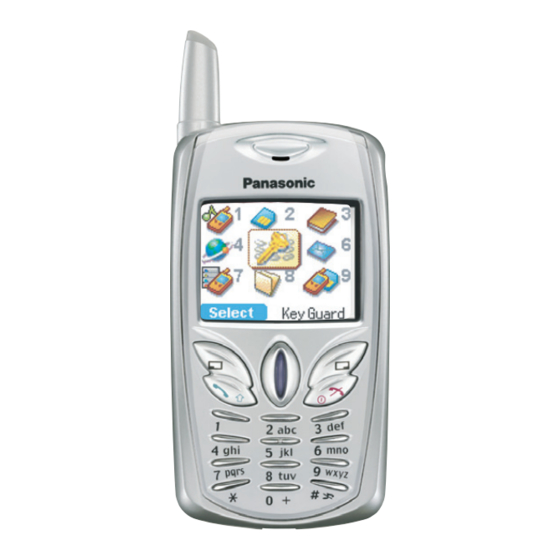
Panasonic EB-G50 Service Manual
Personal cellular telephone
Hide thumbs
Also See for EB-G50:
- Operating instructions manual (104 pages) ,
- Operating instructions manual (88 pages) ,
- Operating instructions manual (88 pages)
Table of Contents
Advertisement
Quick Links
This service information is designed for experienced repair technicians only and is not designed for use by the general public.
It does not contain warnings or cautions to advise non-technical individuals of potential dangers in attempting to service a
product.
Products powered by electricity should be serviced or repaired only by experienced professional technicians. Any attempt to
service or repair the product or products dealt with in this service information by anyone else could result in serious injury or
death.
EB-G50
Frequency Range
TX/RX Frrequency
Separation
RF Channel
Bandwidth
Number of RF
Channels
Speech Coding
Operating
Temperature
Type
RF Output Power
Moduration
WAP
Connection
Voice digitizing
Transmission speed
Signal Reception
Antenna Impedance
(External Connector)
Dimensions
(Excluding antenna)
Weight
Display
Illumination
Keys
SIM
External DC Supply
Voltage
Battery
Standby Time
Talk Time
∗
(
)The network being used, SIM card usage, and the condition of the battery affect Battery life.
Y WARNING
R
Personal Cellular Telephone
900 MHz
TX: 880 MHz –
TX: 1710 MHz –
915 MHz
RX: 925 MHz –
RX: 1805 MHz –
960 MHz
45 MHz
95 MHz
200 kHz
174
374
Full Rate / Enhance Full Rate
-10 °C – +55 °C
Class 4 Handheld
Class 1 Handheld
Max. 32 dBm
Maz. 29 dBm
GMSK
WAP 1.2.1
8 ch / TDMA
13 kbps RPE-LTP / 13 kbps ACLEP
270.833 KBPS
Direct Coversion
50
∗
Height: 77 mm
Width: 43 mm
Max 65 g
Header (1128 x 12 pix)+Body (128 x 96 pix) Bottom (128 x 16 pix)
2 LED for the LCD (Blue Light)
6 LED for the keypad (Blue Light)
18 Physical Keys, 2 Way Navi-Key
3 V Plug-in Only
3.8 V
Standard Li-Ion 720 AHh
∗
78.3-230 Hrs (
)
∗
1.6-7.9 Hrs (
)
ç 2 0 0 3
P a n a s o n i c M o b i l e C o m m u n i c a t i o n s C o . , L t d .
A l l r i g h t s r e s e r v e d . U n a u t h o r i z e d c o p y i n g a n d
d i s t r i b u t i o n i s a v i o l a t i o n o f l a w .
ORDER NO. OMTD030725C8
1800 MHz
1900 MHz
1785 MHz
1850 MHz –
1990 MHz
1880 MHz
80 MHz
300
Class 1 Handheld
Max. 29 dBm
∗
Depth : 16.9 mm
Advertisement
Table of Contents

Related Manuals for Panasonic EB-G50


Summary of Contents for Panasonic EB-G50
- Page 1 ORDER NO. OMTD030725C8 Personal Cellular Telephone EB-G50 900 MHz 1800 MHz 1900 MHz TX: 880 MHz – TX: 1710 MHz – 915 MHz 1785 MHz 1850 MHz – Frequency Range 1990 MHz RX: 925 MHz – RX: 1805 MHz –...
-
Page 2: Table Of Contents
The information contained in this manual and all rights in any design disclosed therein, are and remain the exclusive property of Panasonic Mobile Communications Co., Ltd. Other patents applying to material contained in this publication:... - Page 3 4. TECHNICAL SPECIFICATIONS ..............4-1 4.1.
- Page 4 7. REPAIR PROCEDURES ............... . .7-1 7.1.
-
Page 5: Introduction
They must not be incinerated, or disposed of as ordinary rubbish. 1.1. Purpose of the Manual This Service Manual contains the information and procedures required for installing, operating and servicing the Panasonic GSM Personal Cellular Mobile Telephone system operating on GSM Digital Cellular Networks. -
Page 6: General Description
2.2. Features The Panasonic Telephone Model G50 is a high performance, small, light, handset for business and domestic use. The following features are provided: Dual Codec, which includes Full Rate and Enhanced Full Rate (EFR) Speech Codec. -
Page 7: Operating Instructions
3. OPERATING INSTRUCTIONS 3.1. General This section provides a brief guide to the operation and facilities available on the telephone handset. Refer to the Operating Instructions supplied with the telephone for full operational information. 3.2. Liquid Crystal Display The telephone handset has a graphical chip on glass display. The following icons are available: Status Figure 3.1: Liquid Crystal Display Icon... -
Page 8: Location Of Controls
3.3. Location of Controls Receiver Phone Jack Display Charger Connection The Phone Jack can be used as data transmission port to perform download and test tasks. – 3–2 –... -
Page 9: Concept Of Operation
3.4. Concept of Operation There is a close relationship between the Select keys, Navigation key and display. Main Display Left Hand Selection Area Right Hand Selection Navigation key Soft Key Send and answer Key Power / End Key Navigation Key: Moving up and down through the options in the display area. In idle mode, pressing to enter Own Menu. -
Page 10: Alpha Entry
3.5. Alpha Entry 3.5.1 Character Set / Key Assignments Alpha entry is used to enter alphanumeric characters in to the Phonebook, Short Message and Greeting Message areas. Alphabetic, small / capital letter mode: 12. 13. < > & ç ä à... -
Page 11: Features Structure
3.6. Features Structure Feature Set Listing 1 Telephone Functionality Display and Lighting LCD Display Received Signal Strength Indication Battery Status Icon Call Processing Signal Indication Dialled Number Indication Last Dialed Digit Clear/Entire Line Clear Own Telephone Number Indication Service/No Service Indication Country/PLMN Indication Service Provider Indication Roaming Indication... - Page 12 PIN2 PUK2 Phone Code PIN Check Change PIN FDN Mode (On/Off) ME Personalization Network lock Network Subset Lock Service Provider Lock Corporate Lock SIM Lock Custom IMSI Multiple Lock Sound Settings Ring Tone/Melody (20 predefined, 5 composed, X download) Ring Volume Control (1-5) Alert Type Ring Only Vibration Only...
- Page 13 Reset Setting to Default Hot Key Dial (On/Off) Key 1 to 9 assigned to the Phone-number in SIM or Mobile records from 1 to 9 according to the selection of My Phonebook and press <Send> to dial out Clock Setting Set Time Set Date Display Format...
- Page 14 Line Identification Calling Line Identification Presented (CLIP) Calling Line Identification Restricted (CLIR) Connected Line Identification Restriction (COLP) Connected Line Identification Restriction (COLR) In-Call Menu (Requires Protocol Stack Support) Call on Hold/Swap Answer Second Call Display of Change Advice Information Multiple Call Having Private Conversion With One Participant Dropping One Participant SMS (Requires Carrier and Stack Support)
- Page 15 Send Insert Predefined Text Insert Picture/Melody (EMS MO) Save and Send Message Save Only Auto capital letter in the beginning of string input Predefined Text (15) Edit Preset Message Clear Preset Message to Empty Setup Service Center Number Store SMS Center Number Edit SMS Center Number Message Type Reply Path...
- Page 16 Redial Number Delete Number Call Time Last Call Time Total Sent Total Received Reset Times Call Cost (Requires Protocol Stack Support) Last Call Cost Total Cost Max Cost Reset Counters Set Max Cost Price/Unit GSM 2.30 MMI and GSM 2.90 USSD 2 Optional Network Service (Requires Carrier and Protocol Stack Support) SIM Toolkit Class 1 (SIM Content Update)
- Page 17 Melody Mobile Phonebook Menu Edit Phonebook Number and Name Erase Phonebook Number and Name Speed Dialling (1-9) if mobile phonebook selected as preferred phonebook Copied one or all to SIM Phonebook SIM Phonebook Phonebook Name and Number Storage ADN (Depends on SIM, Max 255) FDN (Number of entries Max 50) SIM Phonebook Menu Edit Phonebook Number and Name...
- Page 18 X downloaded; X depends on the media library's size; The size of a downloaded picture can be variable. Melody manager (20 default. 5 composed, X downloaded) Manage picture list 20 predefined melodies 5 user composed melodies X downloadable, X depends on the Media Library size. Games (WGE) Game 1 Game 2...
- Page 19 - Homepage - Connection Type - Connection Security - IP Address - Linger Time (CSD Bearer) - Dial number - Data Call type - User Name - Password (GPRS Bearer) - APN - User Name - Password - Authentication – 3–13 –...
-
Page 20: Incoming Call Line Identification (Cli)
3.7. Incoming Call Line Identification (CLI) When a call is received the last eight digits of the CLI information is matched with the phonebook. Therefore an incoming call could be matched to the wrong phonebook entry. 3.8. Public Man Machine Interface (MMI) 3.8.1. -
Page 21: Call Line Identification
3.8.7. Call Line Identification Feature Service Code Calling Line Identification Presentation (CLIP) Calling Line Identification Restriction (CLIR) Connected Line Presentation (CLOP) Connected Line Restriction (CLOR) Enable * <SERVICE CODE> * # (SND> Disable # <SERVICE CODE> * # (SND> Temporary Suppress Identification # 31 # <TELEPHONE NUMBER>... -
Page 22: Dial Divert
3.8.9. Dial Divert Call Divert Type Service Code Divert all calls Divert all calls if busy Divert all calls if no reply Divert if not reachable Set Call Bar * * <SERVICE CODE> * <FORWARD TELEPHONE NUMBER> * (Except "No Reply") <TELECOMMUNICATION SERVICE>... -
Page 23: Troubleshooting
3.9. Troubleshooting The user is given the following information and advised to contact the dealer if the problems persist: Problem Cause Remedy Telephone will not Check that the battery pack is fully switch on charged and correctly connected to the telephone. -
Page 24: Important Error Messages
3.10. Important Error Messages The following table is a list of error messages that may occur during use of the telephone, with a description and suggested course of action: Error Message Explanation / Remedy Area not Allowed Roaming in the selected area is not allowed. Network not allowed Roaming with the selected network is not allowed. -
Page 25: Glossary Of Terms
3.12. Glossary of Terms Term Definition DTMF Dual Tone Multiple Frequency tones. The numeric keys 0 to 9, and * and # will generate different DTMF tones when pressed during conversation. These are used to access voice mail, paging and Home banking services. Global System for Mobile communications. -
Page 26: Technical Specifications
4. TECHNICAL SPECIFICATIONS 4.1. Tx Characteristics All data is applicable to E-GSM 900 and GSM 1800 except where stated. 4.1.1. Frequency Error ±0.1 ppm max., relative to base station frequency. 4.1.2 Modulation Phase Error RMS: Equal to or less than 5 ° Peak: Equal to or less than 20 °... -
Page 27: Spurious Emissions At Antenna Connector
4.1.5. Spurious Emissions at Antenna Connector Frequency Filter Approx Limits(dBm) Frequency Range offset Bandwidth Video B/W E-GSM 900 GSM1800/1900 10KHz 30KHz 100KHz to 50MHz 100KHz 300KHz 50 to 500MHz 100KHz 300KHz 500MHz to 1GHz 0 to 1MHz 1 GHz to 12.75 GHz 0 to 10MHz 100KHz 300KHz... - Page 28 GSM 1800/1900 Full Rate Speech The reference sensitivity performance in terms of frame erasure, bit error, or residual bit error rates (whichever is appropriate) is specified in the following table, according to the propagation conditions. Propagation Propagation Propagation Channels Static Conditions conditions conditions conditions...
- Page 29 Blocking: Small MS level in dBµVemf( ) Frequency E-GSM 900 GSM 1800 GSM 1900 FR ± 600 kHz to FR ± 800 kHz FR ± 800 kHz to FR± 1,6 MHz FR ± 1,6 MHz to FR ± 3 MHz 915 MHz to FR - 3 MHz FR ±...
-
Page 30: Technical Description
5. TECHNICAL DESCRIPTION 5.1. RF Overview 5.1.1. Introduction General Specifications The telephone is a Tri-Band product. The transmit and receive bands for the mobile are given in the table below: E-GSM 900 880 - 915 MHz 925 - 960 MHz GSM 1800 1710 - 1785 MHz 1805 - 1880 MHz... -
Page 31: Rf Function Block
5.1.2. RF Function Block Figure 5.1. : RF Function Block Diagram – 5–2 –... -
Page 32: Functional Description
RF LO always requires external frequency sources with VCTCXO in VE2. And LO frequency is periodically re-tuning to synchronize with cell or network. Antenna EB-G50 uses Helical-type antenna, which is most low-cost, monopole-like antenna. The antenna takes different spacing to define bands of GSM, DCS and PCS. – 5–3 –... - Page 33 Transceiver - - Transmitter Antenna Base-band Power Coupler section Detector TX IN I/Q PA gain controller 3-wire bus PAVAPC – TXVCO TX IN 1800/1900 UHF synthesizer Figure 5.3. Transmitter block diagram TX path is a translation loop architecture consisting of an IQ modulator, integrated high power VCO, offset mixer, programmable divider, PFD, charge pump, and power amplifier with its control circuit.
- Page 34 Transceiver - - Receiver RX LO source from chip Antenna RF SAW FILTER RXIN RXIP Switch & Display RXQN RXQP 1800 1900 DCOC Figure 5.4. Receiver block diagram RX path is a direction down conversion architecture that eliminates the need for Intermediate Frequency (IF) components. The device includes three bands integrated LNAS, a quadrate demodulator, baseband amplifier circuit with I/Q outputs and three stages of DC-offset correction.
-
Page 35: Baseband Overview
PJ_FUNC_SEL Figure 5.5. Baseband Block Diagram The EB-G50 Baseband is built around a GSM chipset developed by Advanced Device. One chip (AD6525) carries out signal processing with DSP and CPU, and the other chip (AD6521) provides the analogue interface. The highly integrated nature of the chips means that each contains a large number of functions. -
Page 36: Digital Baseband Processor
5.2.2. Digital Baseband Processor GSM processor ADI AD6525 Package 160 -Ball LFBGA Feature Complete single chip GSM Programmable Digital Baseband Processor divided into three main subsystems: 1.Control processor subsystem including 32-bit MCU ARM7TDMI control processor 39 MHz operation at 1.8V 1Mb on-chip System SRAM Memory 2. - Page 37 5.2.3. Keypad The Keypad has a 4 x 5 matrix, allowing 18 keys to be scanned. When a key being pressed, a keypad interrupt is generated. To find which key has been pressed, the software scans each column in turn and reads which row is active. Because of key bounce, the key press is confirmed twice at approximately 40-60 ms intervals.
-
Page 38: Cpu Memory
5.2.5. CPU Memory To reduce component space, the phone uses a BGA package with Dual operation Flash memory and SRAM MCP. The following memory configuration is used: 64Mbits Flash memory organized as 4M * 16bits or 8M * 8bits 32Mbits Pseudo RAM organized as 2M * 16 bits 5.2.6. -
Page 39: Audio System
5.3. Audio System VINNOR P/N A,V,B ADC/DAC serial Port VOUTNOR P/N VoiceBand Receiver & VINAUX P/N BaseBand Codec. GSM Processor (AD6521) Phone Audio (AD6525) VOUTAUX P/N Jack Buzzer(L_SPK Mode) HPOUT GPIO5 Meledy IC Speaker Control /Data Interface LDO 3.0V Figure 5.9. Audio system block diagram AD6521 is a Voiceband Baseband Codec (VBC) that combines, onto a single chip, all A/D and D/A converters that are necessary to build a complete GSM, DCS1800, and PCS1900 mobile radio. -
Page 40: Microphone
Individual Power Management Features Baseband, Voiceband and Auxiliary Serial Ports JTAG Interface Optimized Low-Power Converter Design Low 1.6V Digital Supply Operation Variable Digital Interface Supply Low 2.4V Analog Supply Operation Figure 5.10. AD6521 Functional Block Diagram 5.3.2. Microphone The microphone is a noise canceling type to provide improved speech pick-up, noise immunity and reduced echo. -
Page 41: Receiver
5.3.3. Receiver The GSM Standard requires that the receiver audio frequency response must fit within the mask shown below. Figure 5.12. Handheld GSM Receive Audio Frequency Response The phone is designed to meet requirements with a Type 1 artificial ear. Volume Level Volume Total Gain... - Page 42 5.5. Power Management Subsystem In base-band power management, ADI ADP3522 is designed for all base-band main power supply. It provides six regulator outputs for VCORE (1.8V), VMEM (2.8V), VANA (2.55V), VRTC (1.95V), VCTCXO (2.75V), SIMVCC (2.85V). VCORE and VMEM provide all digital power and VANA provides all analog power. VRTC is used to charge Li-Mn coin cell for real time clock, and VCTCXO is the power source of 13MHz clock buffer.
-
Page 43: Power System Ship
5.5.1. Power System Ship Chipset ADI ADP3522 Package 32-pin LFCSP5x5 FEATURES Handles all GSM Baseband Power Management Six LDOs Optimized for Specific GSM Subsystems Li-Ion Battery Charge Function Optimized for the AD20msp430 Baseband Chipset Reduced Package Size: 5x5 mm LFCSP-32 ADP3522 is specified over the temperature range of –20 °C to +85 °C. -
Page 44: Power On / Off Control
5.5.3. Power On / Off Control The ADP3522 handles all issues regarding the powering ON and OFF of the handset. It is possible to turn on the ADP3522 in three different ways: 8 Pulling the PWRONKEY Low 8 Pulling PWRONIN high 8 CHRIN exceeds CHRDET threshold Pulling the PWRONKEY low is the normal way of turning on the handset. -
Page 45: Battery Charging And Monitoring
5.6. Battery Charging and Monitoring 5.6.1. Charging Current The status of the LCD battery icon is determined by the value of ADC0 returned from AD6521, as indicated in the table: Battery Pack Li-lon 3 bar 3.65 V < < 3.95 V 2 bar 3.54 V <... -
Page 46: Disassemby / Reassemby Instructions
6. DISASSEMBLY / REASSEMBLY INSTRUCTIONS 6.1. General This section provides disassembly and reassembly procedures for the main components of the telephone. These assemblies MUST be performed by qualified service personnel at an authorized service center. The following Warnings and Cautions MUST be observed during all disassembly / reassembly operations: WARNING The equipment described in this manual contains polarized capacitors utilizing liquid electrolyte. -
Page 47: Disassemby
6.2. Disassembly 1. Take out the Antenna Knob by tweezers. 2. Push the Battery Knob up to remove the battery and unscrew 2 screws on the Base Case. 3. Carefully prise apart the Upper Case and Bottom Case, creating a gap around the DC Jack. Insert the separation tool into the gap ceated, and gently slide the tool in the direction as shown, ensuring that the moduled hocks separate all the way. - Page 48 4. Take out the Upper Case and unscrew 1 screw located on PCB-A. 5. Carefully lift PCB-A from right side and pull out the Vibrator Cable to completely separate from the PCB- and the base Unit. 6. Take out the Receiver Rubber. –...
- Page 49 7. Remove the Microphone. 8. Unsolder the hook of Shield-Key (on top of the RTC) and detach from the PCB-A. 9. Gently separate the glue in both sides and remove the Shield-Key. – 6–4 –...
- Page 50 10. Gently prise two ears of the LCD Module to separate it from the PCB-A.. 11. Carefully lift up the connector cover to vertical to take out the LCD Module. 12. Remove the Key Set from the Upper Case. – 6–5 –...
- Page 51 13. Remove the MIC Holder from the Base Case. 14. Lift the Vibrator and Speaker from the Base Case by inserting small blunt object underneath them. 15. Narrow the hooks of the Antenna Ass'y, push upward and take it out. –...
- Page 52 16. Carefully narrow the Battery Knob by pressing both hooks from internal side of the Base Case push the hooks downward to slide out. 17. Pull down the Battery Knob from outside to completely remove. 18. Take out the Battery Knob Spring. –...
- Page 53 6.3. Reassembly 1. Put the Battery Knob Spring back. 2. Locate the Battery Knob in the middle and push upward to the top and release. make sure the Knob keep normal flexibility. 3. Push the Antenna Ass'y downward until the hooks are fixed probably. –...
- Page 54 4. Utilize the bulge to put the Speaker and Vibrator back into the fillister. 5. Fix the MIC Holder in the Base Case as shown. 6. Put the Shield_Top and Shield-SIM-Holder back. If the shields are out of shape, replace a new one.
- Page 55 7. Insert the MIC into the PCB-A by aligning pins in down sides. 8. Carefully insert the LCD Cable, close the connector cover and attach the LCD Module. 9. Cover Shield-Key and solder the hook (on top of the RTC) to ensure complete performance. –...
- Page 56 10. Cover the Receiver with the Receiver Rubber. 11. Insert the Vibrator Cable into connector and organize the Cable to avoid stuck. 12. Put the PCB-A into the Base Case from the Phone Jack side. Make sure the PCB-A located probably. –...
- Page 57 13. Tighten the screw on the PCB-A. 14. Assemble the Upper Case by combining from top. 15. Carefully press along both sides to make sure the casing fixed probably. Check the side caps are within specifications. – 6–12 –...
- Page 58 16. Tighten 2 screws on the Case and put the Antenna Rubber in the hole. – 6–13 –...
-
Page 59: Repair Procedures
7. REPAIR PROCEDURES 7.1. Introduction This section provides information on testing the telephone. Thelayout is as follows: Section 7.2. : Lead Free (PbF) solder: Identification and repair of PCBs using PbF solder. Section 7.3. : External testing: describes equipment requirements and general set up procedure. Section 7.4. - Page 60 PCB Repair Jig (Part No. 3WZ001102AAA) The PCB Repair Jig provides the necessary connections between the PCB Assembly and external test equipment. It is required for RF calibration. Figure 7.1. : PCB Repair Jig A cable with SMA female connector is provided to make the RF connection. An SMA to N-Type male adaptor will be required to connect the Repair Jig to the service equipment.
- Page 61 DL Cable (Part No. DD0VE2TH004) DL Cable is used for software download and TX Power/RX RSSI calibration with dummy battery. Figure 7.3. : DL Cable RF Cable (Part No. 3WZ001103AAA) The RF cable provides the necessary connections between the PCB Repair Jig/RF Adapter and external test equipment. Figure 7.4.
- Page 62 Dummy Battery (Part No. 3WZ001104AAA) Dummiy battery is used for software download and Battery calibration. Figure 7.6. : Dummy Battery GSM Tester This unit acts as a base station providing all the necessary GSM signalling requirements and also provides GSM signal measuring facilities.
-
Page 63: Test Equipment Setup
7.4. Test Equipment Setup 7.4.1. Equipment Required PCB Repair Jig RF Cable DL Cable Tester 3.8 V DC Dummy Power Battery Supply PCB TEST SETUP Handset RF Cable Tester DL Cable 3.8 V DC Dummy Power Battery Supply COMPLETE UNIT TEST SETUP Figure 7.7. -
Page 64: Software Downloard & Adjustment Procedure
. SOFTWARE DOWNLOAD & ADJUSTMENT PROCEDURE 8.1. Service Software Upgrade Equipment setting for single downloading: Handset RS232 D/L Cable 1. Install the download tool on PC. 2. Keep the handset off. make sure the correct target file (*.mbf) is ready. (Please make sure the capacity of battery is enough during downloading.) –... - Page 65 3. Execute main program (In the first time or target file is removed, it will show "File not found".) The program will detect how many ports are available on PC. 3-1 Select download function. 3-2 Click the wheel icon and select the target file. 3-3 Long press on the power key and follow the indication on screen.
-
Page 66: Mmi Test
8.2. MMI Test In EB-G50, the repair technicians can dial *#369# on handset under normal operating condition to check or adjust the below functions. Please notice the items 4,5,7 are for production and for special purpose, don't change the default value arbitrarily or may cause mobile malfunction. -
Page 67: Adjustment Procedure
8.3. ADJUSTMENT PROCEDURE 8.3.1. Equipment Setting for TX/RX adjustment 1. Connect all equipments as above. 2. Please set the cable loss within the GSM tester before proceeding to any tests. It's recommended that each band (GSM 900 /DCS 1800/PCS 1900) tested separately. 3. -
Page 68: Test Operation Procedure
8.3.3. Test Operation Procedure Execute the main program "PAC CalTool V3.0.exe" Enter Test 1. Select the related "PORT", "MODEL". 2. Click [ENTER TEST MODE]. 3. If successful, the information dialog will pop up witin 3 sec and click [OK]. – 8–5 –... - Page 69 TX Test Power Control Level GSM 900 Power Transmitter Tolerances Control Level Output Power Normal Extreme 19-31 PCS 1900 DCS 1800 Power Transmitter Power Transmitter Tolerances Tolerances Control Level Output Power Control Level Output Power Normal Extreme Normal Extreme 22-29 Reserved Reserved Reserved...
- Page 70 There are two parts in this test item. (1) TX POWER SCALING FACTOR 1. Click [Read] to read the values inside the handset as reference. 2. Select "BANDMODE", EGSM_DCS for 900/1800, EGSM_PCS for 1900 3. Enter the ARFCN of each middle band-> click [APPLY] (ex: EGSM–37) and set tester in the same channel.
- Page 71 (2) TX FREQ COMPENSATION 1. Select "BANDMODE", EGSM_DCS for 900/1800, EGSM_PCS for 1900 2. Enter the first ARFCN listed in CH column -> click [APPLY] and set tester in the same channel. 3. Enter the estimate value in SCALING FACTOR -> click [APPLY] and read the TX output power value on the tester.
- Page 72 RX Test There two parts in this test item. (1) RX POWER SCALING FACTOR Set tester as (a) Test Function: CW (b) RF Gen Power: -60dbm (c) MS TX Level: 5 1. Click [Read] to read the values inside the handset as reference. 2.
- Page 73 (2) RX FREQ COMPENSATION Set tester as (a) Test Function: CW (b) RF Gen Power: -60dbm (c) MS TX Level: 5 1. Select "BANDMODE", EGSM_DCS for 900/1800, EGSM_PCS for 1900 2. Enter the first ARFCN in the CH column and plus 0.0677MHz to tester's RF Gen Freq in the related. 3.
-
Page 74: Battery
8.3.4. Battery Equipment setting for battery adjustment Notice: 1.Change the handset comport setting: *#369#->Com port->GENIE before process. 2.Remember to set the handset comport setting back to ÅgOffÅh after adjustment, or it will cause malfunction to earphone. Operation Process 1. Click [Read] to read the values inside the handset as reference. 2. -
Page 75: Replacement Parts List
9. REPLACEMENT PARTS LIST 9.1. Case and Cover Parts Ref. No Description Sliver Blue 1MIZZZZPAG8 1MIZZZZPAH6 1MIZZZZPAI4 Upper Case + Panal (BPMF) Upper Case + Panel (Standard) 1MIZZZZPAJ1 1MIZZZZPAK9 1MIZZZZPAL7 1MIZZZZPA19 1MIZZZZPA27 1MIZZZZPA35 Upper Case + Panel (Stroke) Upper Case + Panel (Thai) 1MIZZZZPAM5 1MIZZZZPAN3 1MIZZZZPAP1... -
Page 76: Main Pcb Assembly
9.2. Main PCB Assembly Cct Ref Part No. Part Name & Description Grid Cct Ref Part No. Part Name & Description Grid AN1161 DFHD01MS101 CONN SMD SPRING HD 1P 1R MS(P2.3,H7.3) C1116 CH03306JBD7 CERAMIC CAPACITOR 33pF 50V B1221 CX1HB102001 EMI FILTER CHIP BLM11HB102SDPT C1141 CH03906JBD9 CERAMIC CAPACITOR... - Page 77 Cct Ref Part No. Part Name & Description Grid Cct Ref Part No. Part Name & Description Grid L301 CV-2201KN16 INDUCTOR CHIP 2.2uH R1203 CS12202FB06 FIXED RESISTOR 220O 1/16W L1102 CVB4703TN04 INDUCTOR CHIP 4700pH R1204 CS13902JB06 FIXED RESISTOR 390O 1/16W L1142 CH+5006TB07 CERAMIC CAPACITOR...
-
Page 78: Mmi (Keyboard) Pcb Assembly
9.3. MMI (Keyboad) PCB Assembly Cct Ref Part No. Part Name & Description Grid Cct Ref Part No. Part Name & Description Grid CH03306JBD7 CERAMIC CAPACITOR 33pF 50V C531 CH03306JBD7 CERAMIC CAPACITOR 33pF 50V C532 CH03306JBD7 CERAMIC CAPACITOR 33pF 50V C733 CH41002KB93 CERAMIC CAPACITOR... -
Page 80: Rf Block Diagram
10.2. RF Block Diagram LNA900I LNA1800I LNA1900I LOGE DATA,CLK Frrc- UVTUN N PLL 26MHz LOGE VTCXO CX77314 TXI- TXVC TLCPO CX74063 – 10–2 –...
Need help?
Do you have a question about the EB-G50 and is the answer not in the manual?
Questions and answers